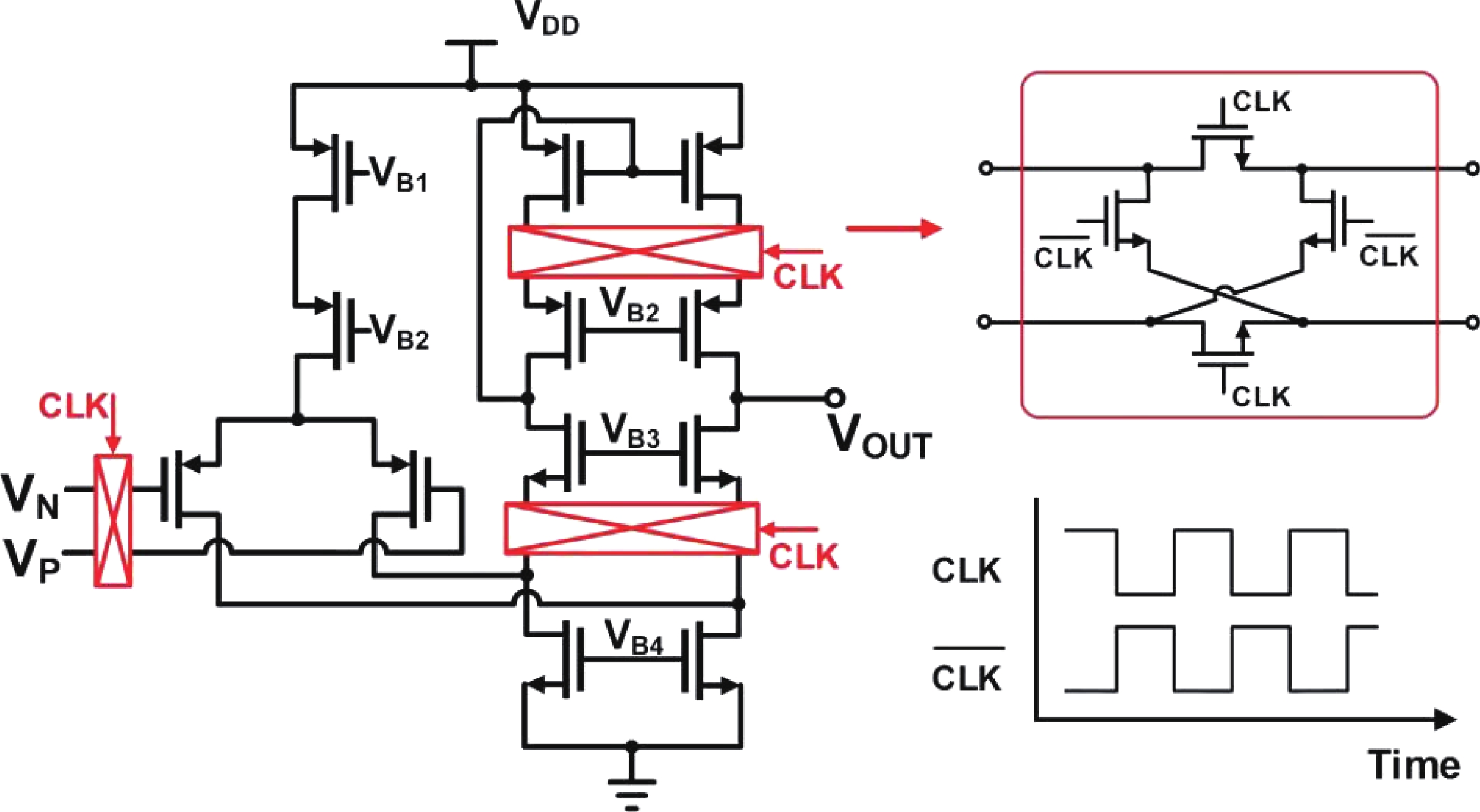
Fig. 1.
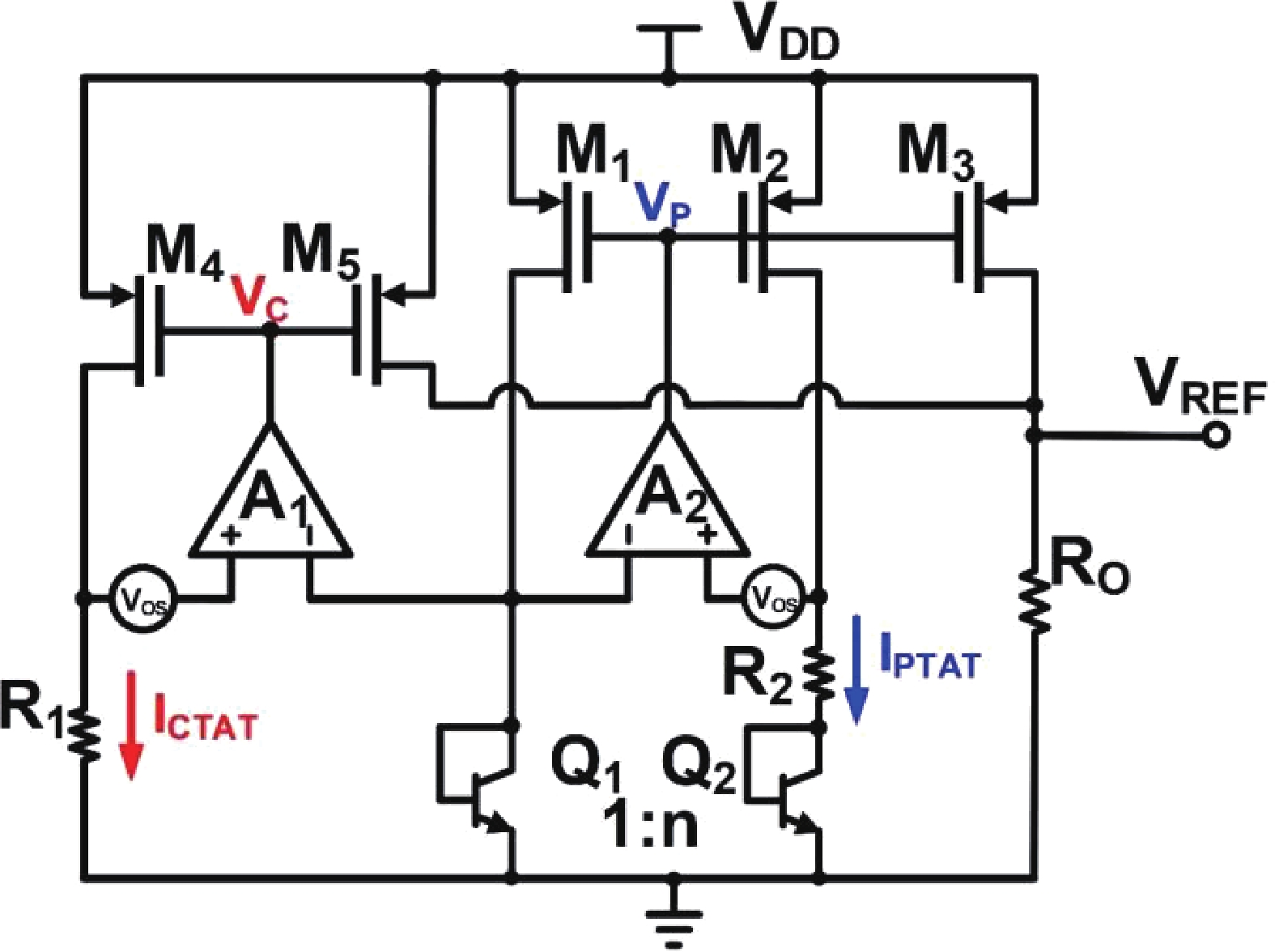
(Color online) The current mode BGR core.
SPECIAL TOPIC ARTICLES
Jing Wang1, Feixiang Zhang1, Zhiyuan He1, Hui Zhang2 and Lin Cheng1,
Corresponding author: Lin Cheng, eecheng@ustc.edu.cn
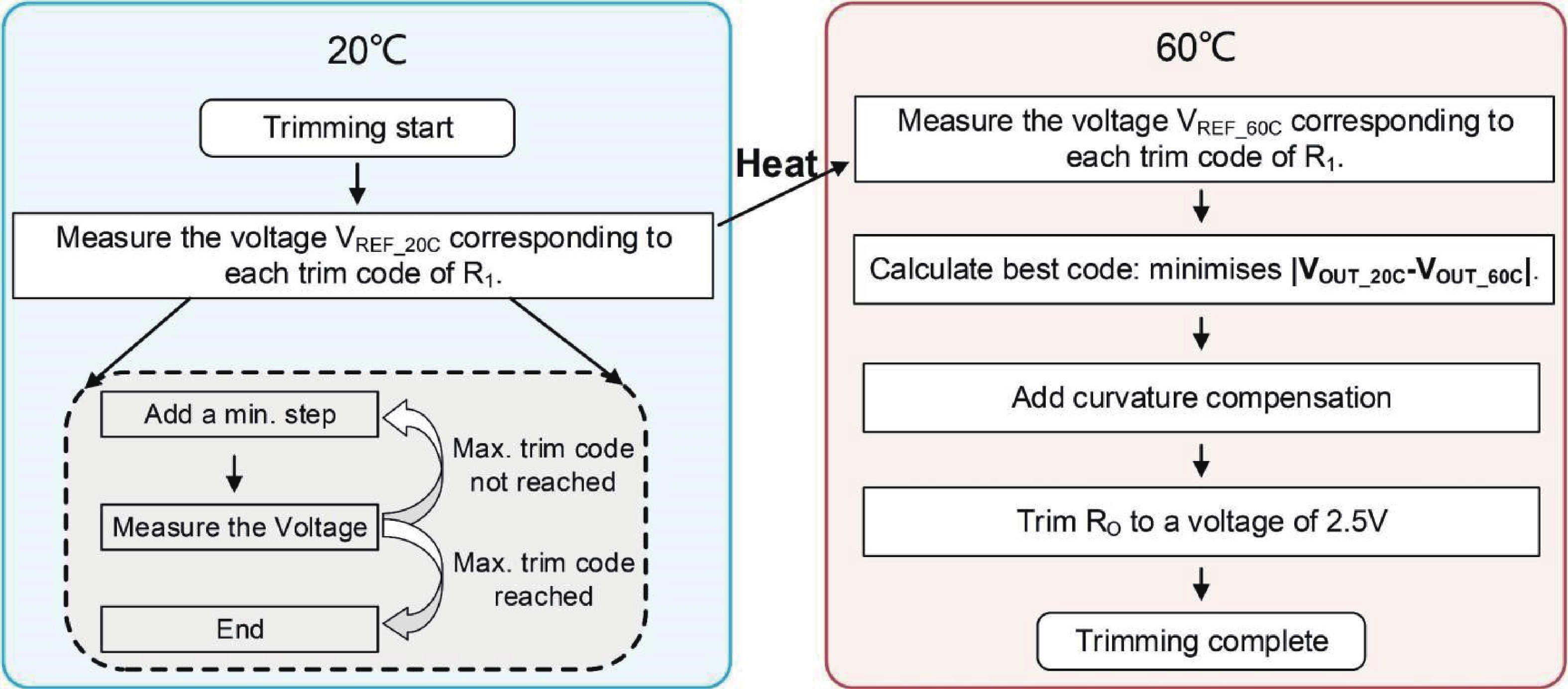
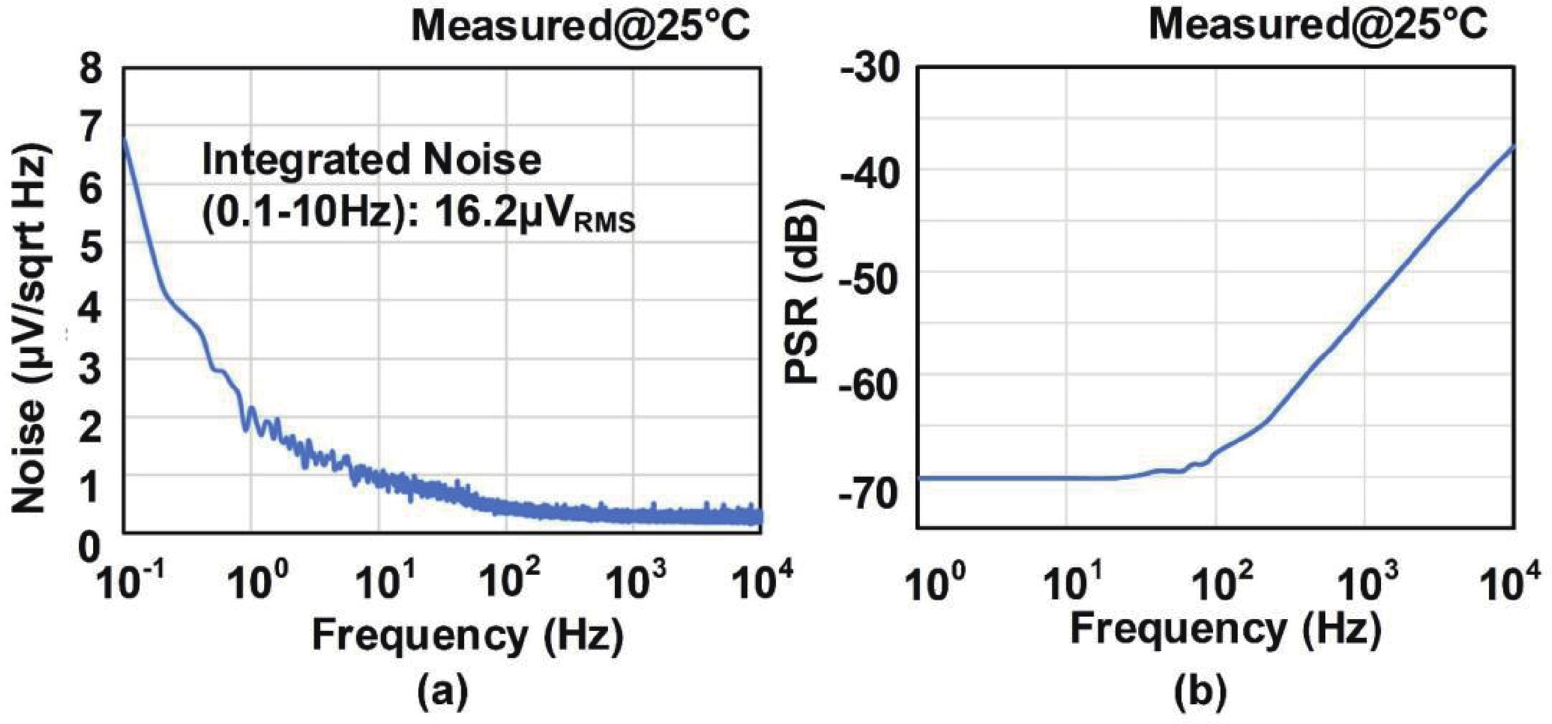
Abstract: This paper introduces a high-precision bandgap reference (BGR) designed for battery management systems (BMS), featuring an ultra-low temperature coefficient (TC) and line sensitivity (LS). The BGR employs a current-mode scheme with chopped op-amps and internal clock generators to eliminate op-amp offset. A low dropout regulator (LDO) and a pre-regulator enhance output driving and LS, respectively. Curvature compensation enhances the TC by addressing higher-order nonlinearity. These approaches, effective near room temperature, employs trimming at both 20 and 60 °C. When combined with fixed curvature correction currents, it achieves an ultra-low TC for each chip. Implemented in a CMOS 180 nm process, the BGR occupies 0.548 mm² and operates at 2.5 V with 84 μA current draw from a 5 V supply. An average TC of 2.69 ppm/°C with two-point trimming and 0.81 ppm/°C with multi-point trimming are achieved over the temperature range of −40 to 125 °C. It accommodates a load current of 1 mA and an LS of 42 ppm/V, making it suitable for precise BMS applications.
Keywords: bandgap reference, high precision, low temperature coefficient, small line sensitivity, battery management system, BMS
| [1] |
Zhu G Q, Yang Y T, Zhang Q D. A 4.6-ppm/°C high-order curvature compensated bandgap reference for BMIC. IEEE Trans Circuits Syst II Express Briefs, 2019, 66(9), 1492 doi: 10.1109/TCSII.2018.2889808
|
| [2] |
Hunter B L, Matthews W E. A ± 3 ppm/°C single-trim switched capacitor bandgap reference for battery monitoring applications. IEEE Trans Circuits Syst I Regul Pap, 2017, 64(4), 777 doi: 10.1109/TCSI.2016.2621725
|
| [3] |
Boo J H, Cho K I, Kim H J, et al. A single-trim switched capacitor CMOS bandgap reference with a 3σ inaccuracy of 0.02%, −0.12% for battery-monitoring applications. IEEE J Solid State Circuits, 2021, 56(4), 1197 doi: 10.1109/JSSC.2020.3044165
|
| [4] |
Ma Y L, Bai C F, Wang Y, et al. A low noise CMOS bandgap voltage reference using chopper stabilization technique. 2020 IEEE 5th International Conference on Integrated Circuits and Microsystems (ICICM), 2020, 184 doi: 10.1109/ICICM50929.2020.9292198
|
| [5] |
Duan Q, Roh J. A 1.2-V 4.2-ppm/°C high-order curvature-compensated CMOS bandgap reference. IEEE Trans Circuits Syst I Regul Pap, 2015, 62(3), 662 doi: 10.1109/TCSI.2014.2374832
|
| [6] |
Ge G, Zhang C, Hoogzaad G, et al. A single-trim CMOS bandgap reference with a 3σ inaccuracy of ±0.15% from –40°C to 125°C. 2010 IEEE International Solid-State Circuits Conference-(ISSCC), 2010, 46(11), 2693 doi: 10.1109/JSSC.2011.2165235
|
| [7] |
Zhou Z K, Shi Y, Huang Z, et al. A 1.6-V 25-μA 5-ppm/°C curvature-compensated bandgap reference. IEEE Trans Circuits Syst I Regul Pap, 2012, 59(4), 677 doi: 10.1109/TCSI.2011.2169732
|
| [8] |
Maderbacher G, Marsili S, Motz M, et al. 5.8 A digitally assisted single-point-calibration CMOS bandgap voltage reference with a 3σ inaccuracy of ±0.08% for fuel-gauge applications. 2015 IEEE International Solid-State Circuits Conference-(ISSCC) Digest of Technical Papers, 2015, 1 doi: 10.1109/ISSCC.2015.7062946
|
| [9] |
Sheng J G, Chen Z L, Shi B X. A 1V supply area effective CMOS Bandgap reference. 2003 5th International Conference on ASIC Proceedings, 2003, 619 doi: 10.1109/ICASIC.2003.1277625
|
| [10] |
Chen H M, Lee C C, Jheng S H, et al. A sub-1 ppm/°C precision bandgap reference with adjusted-temperature-curvature compensation. IEEE Trans Circuits Syst I Regul Pap, 2017, 64(6), 1308 doi: 10.1109/TCSI.2017.2658186
|
| [11] |
Chen K, Petruzzi L, Hulfachor R, et al. A 1.16-V 5.8-to-13.5-ppm/°C curvature-compensated CMOS bandgap reference circuit with a shared offset-cancellation method for internal amplifiers. IEEE J Solid State Circuits, 2021, 56(1), 267 doi: 10.1109/JSSC.2020.3033467
|
| [12] |
Meijer G C M, Schmale P C, Van Zalinge K. A new curvature-corrected bandgap reference. IEEE J Solid State Circuits, 1982, 17(6), 1139 doi: 10.1109/JSSC.1982.1051872
|
| [13] |
Liu L X, Liao X F, Mu J C. A 3.6 μVrms noise, 3 ppm/°C TC bandgap reference with offset/noise suppression and five-piece linear compensation. IEEE Trans Circuits Syst I Regul Pap, 2019, 66(10), 3786 doi: 10.1109/TCSI.2019.2922652
|
| [14] |
Huang S L, Li M D, Li H, et al. A sub-1 ppm/°C bandgap voltage reference with high-order temperature compensation in 0.18-μm CMOS process. IEEE Trans Circuits Syst I Regul Pap, 2022, 69(4), 1408 doi: 10.1109/TCSI.2021.3139908
|
| [15] |
Liu N Q, Geiger R L, Chen D G. Sub-ppm/°C bandgap references with natural basis expansion for curvature cancellation. IEEE Trans Circuits Syst I Regul Pap, 2021, 68(9), 3551 doi: 10.1109/TCSI.2021.3096166
|
| [16] |
Jiang J Z, Shu W, Chang J S. A 5.6 ppm/°C temperature coefficient, 87-dB PSRR, sub-1-V voltage reference in 65-nm CMOS exploiting the zero-temperature-coefficient point. IEEE J Solid State Circuits, 2017, 52(3), 623 doi: 10.1109/JSSC.2016.2627544
|
| [17] |
Zhou Z K, Shi Y, Wang Y, et al. A resistorless high-precision compensated CMOS bandgap voltage reference. IEEE Trans Circuits Syst I Regul Pap, 2019, 66(1), 428 doi: 10.1109/TCSI.2018.2857821
|
| [18] |
Wang R C, Lu W G, Zhao M, et al. A sub-1ppm/°C current-mode CMOS bandgap reference with piecewise curvature compensation. IEEE Trans Circuits Syst I Regul Pap, 2018, 65(3), 904 doi: 10.1109/TCSI.2017.2771801
|
| [19] |
Ma B, Yu F Q. A novel 1.2–V 4.5-ppm/°C curvature-compensated CMOS bandgap reference. IEEE Trans Circuits Syst I Regul Pap, 2014, 61(4), 1026 doi: 10.1109/TCSI.2013.2286032
|
| [20] |
Liao X F, Zhang Y X, Zhang S H, et al. A 3.0 μ vrms, 2.4 ppm/°C BGR with feedback coefficient enhancement and bowl-shaped curvature compensation. IEEE Trans Circuits Syst I Regul Pap, 2024, 71(5), 2424 doi: 10.1109/TCSI.2024.3373788
|
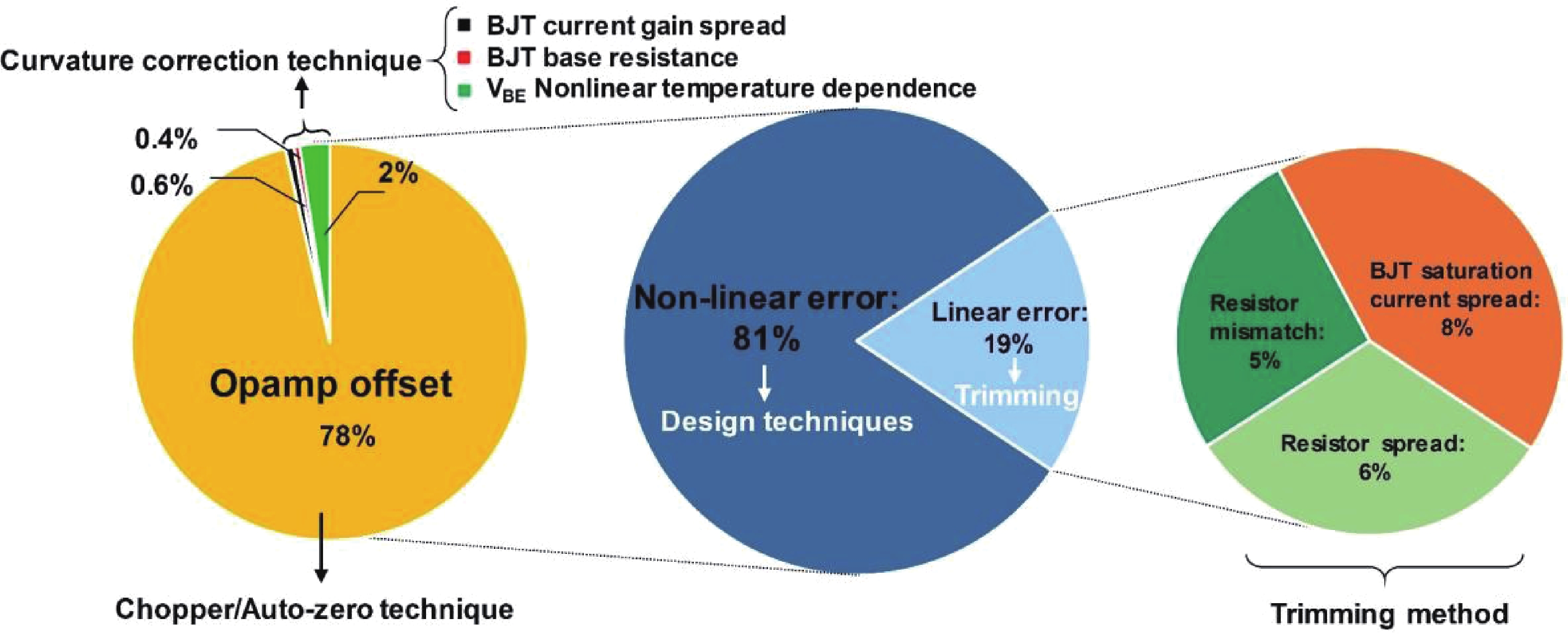
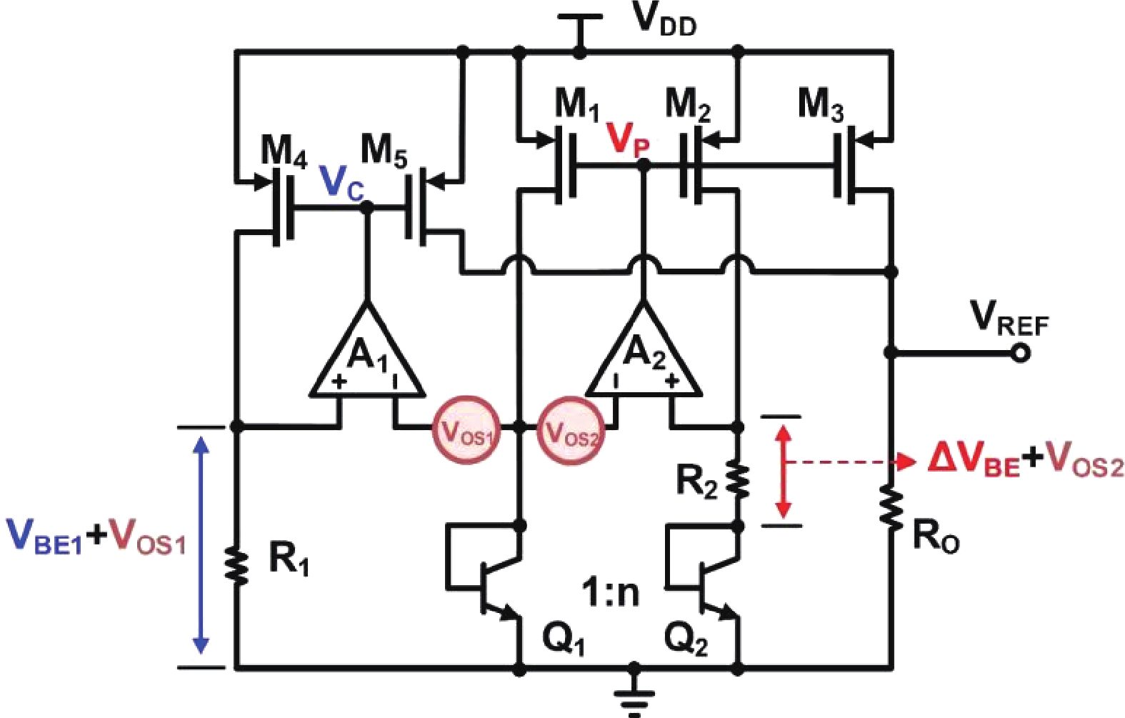
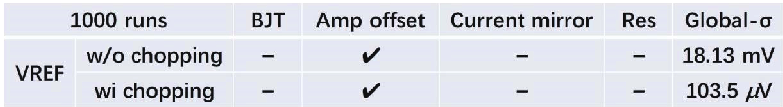
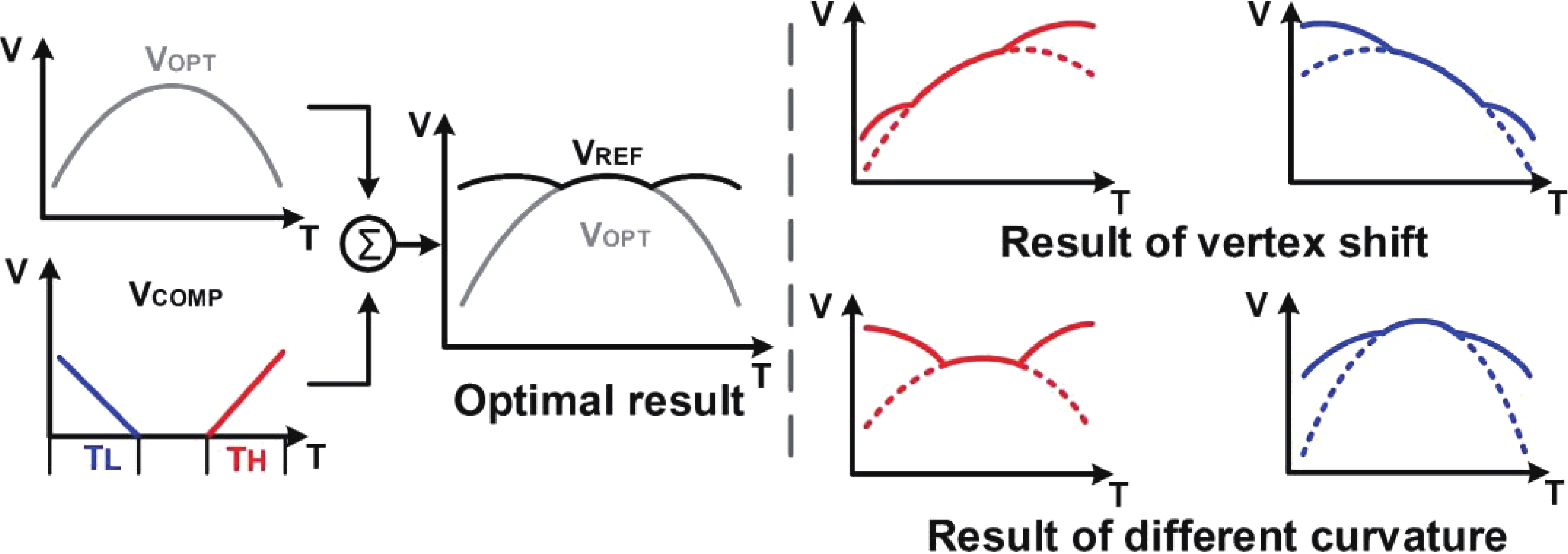
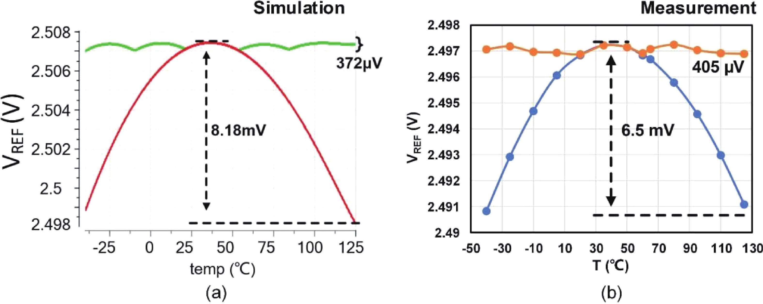
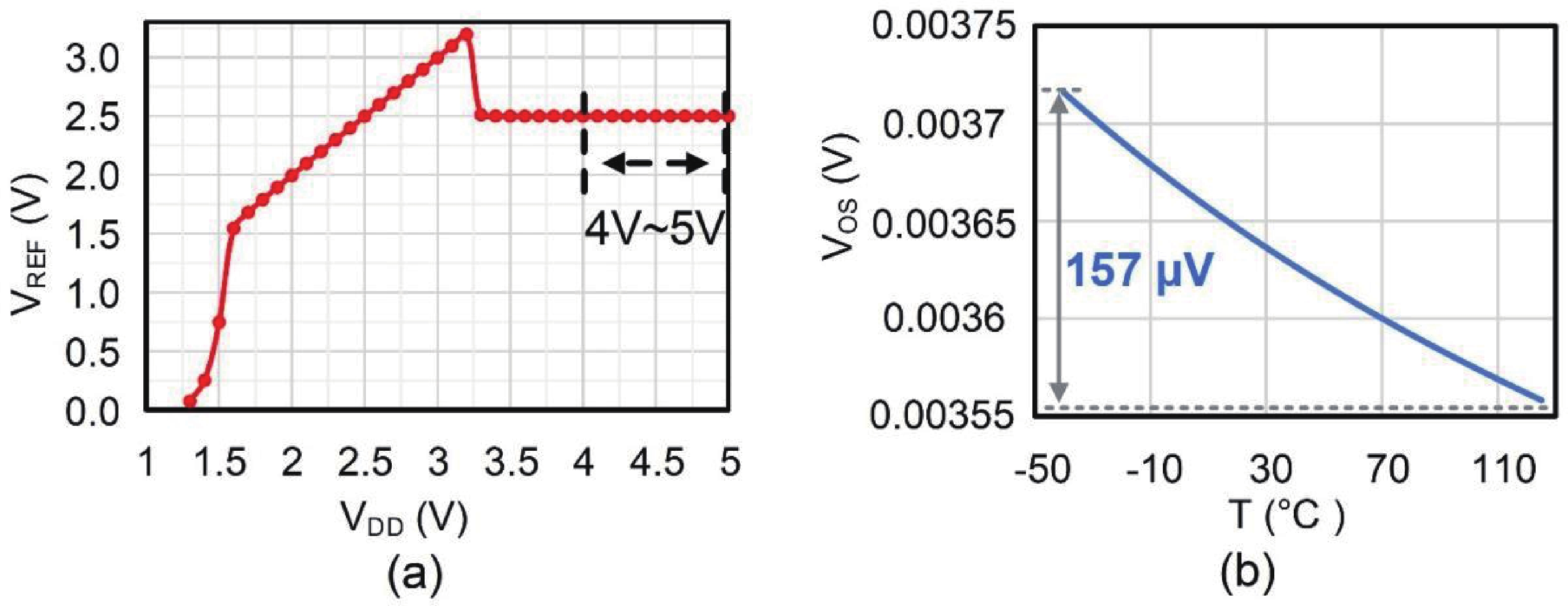
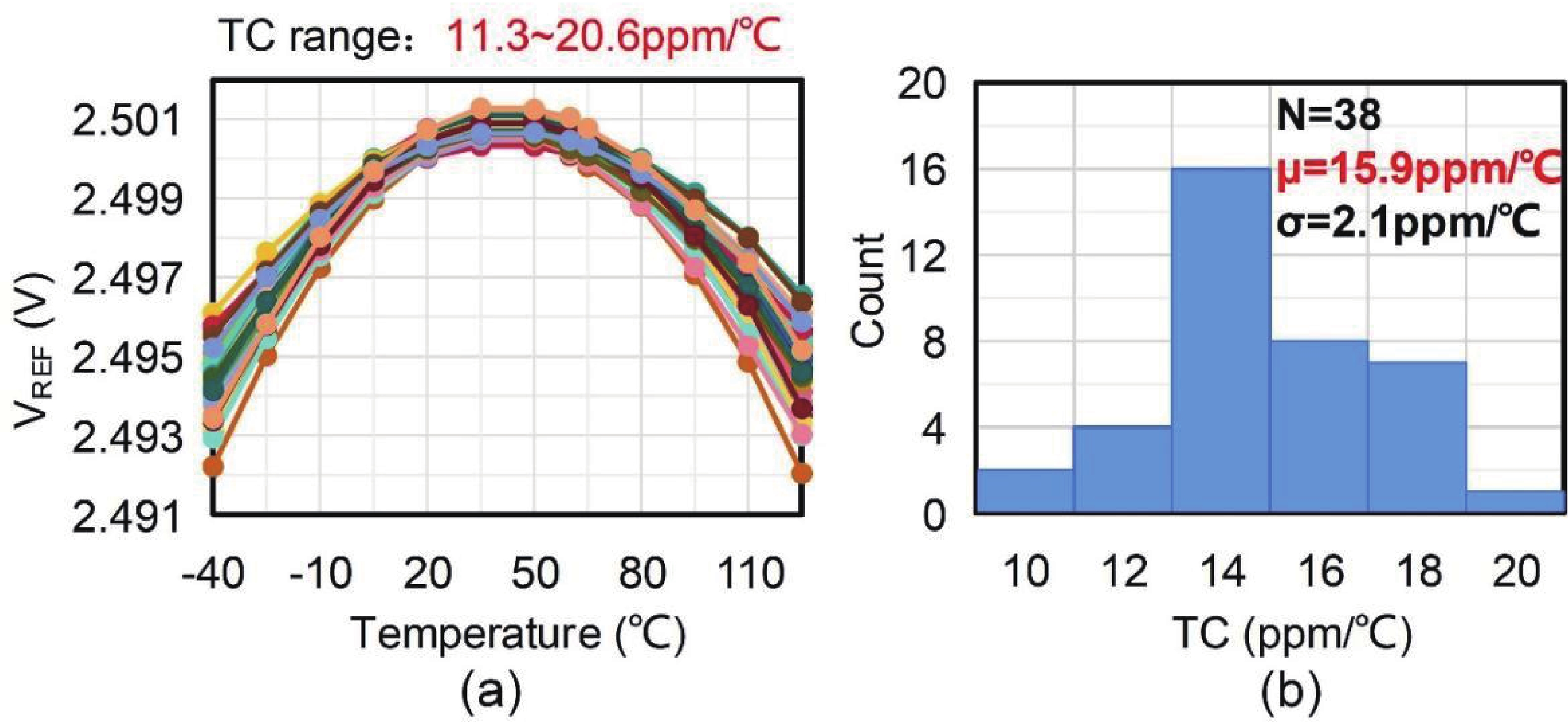
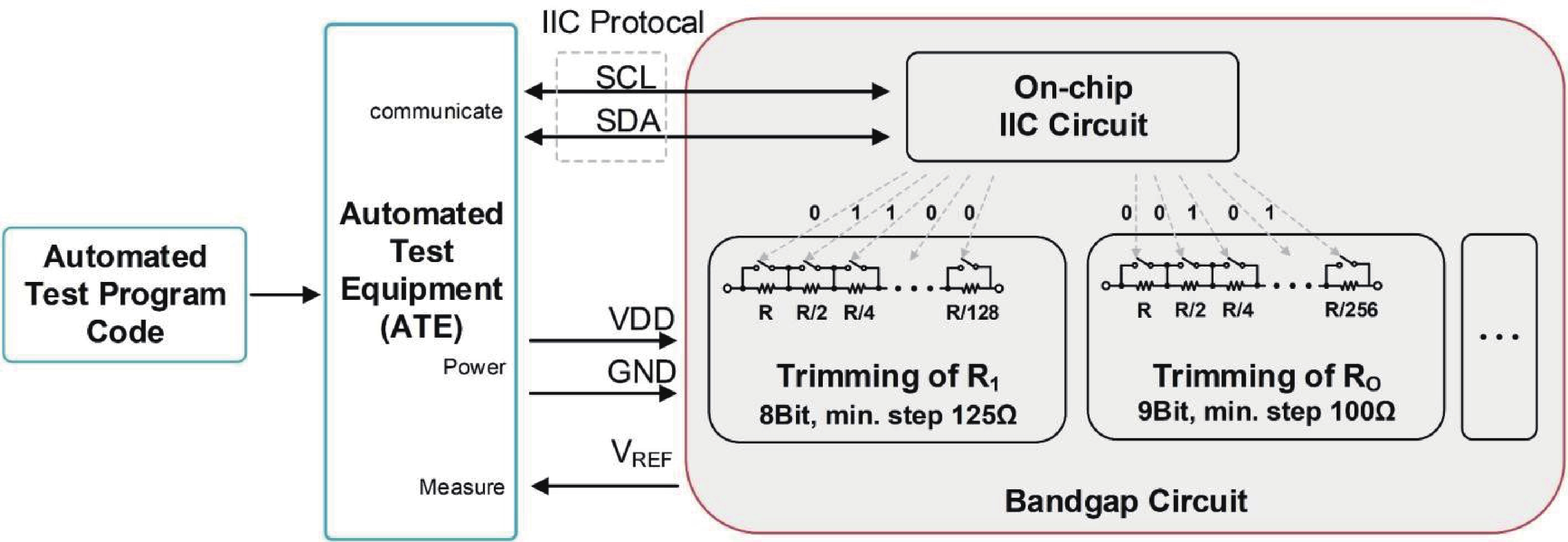
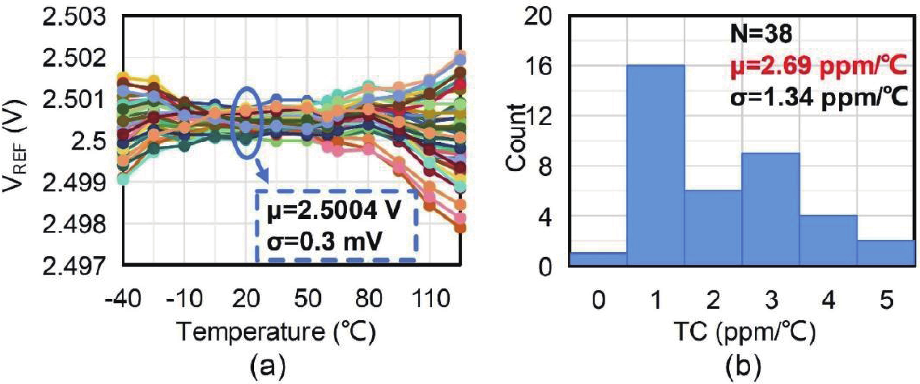
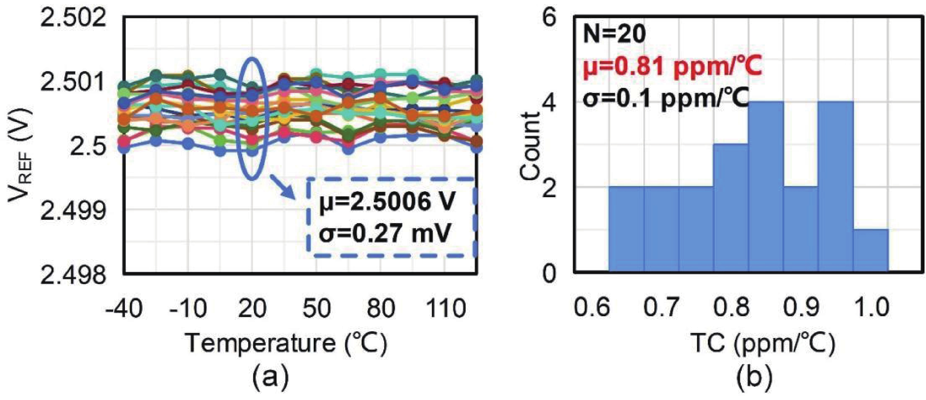
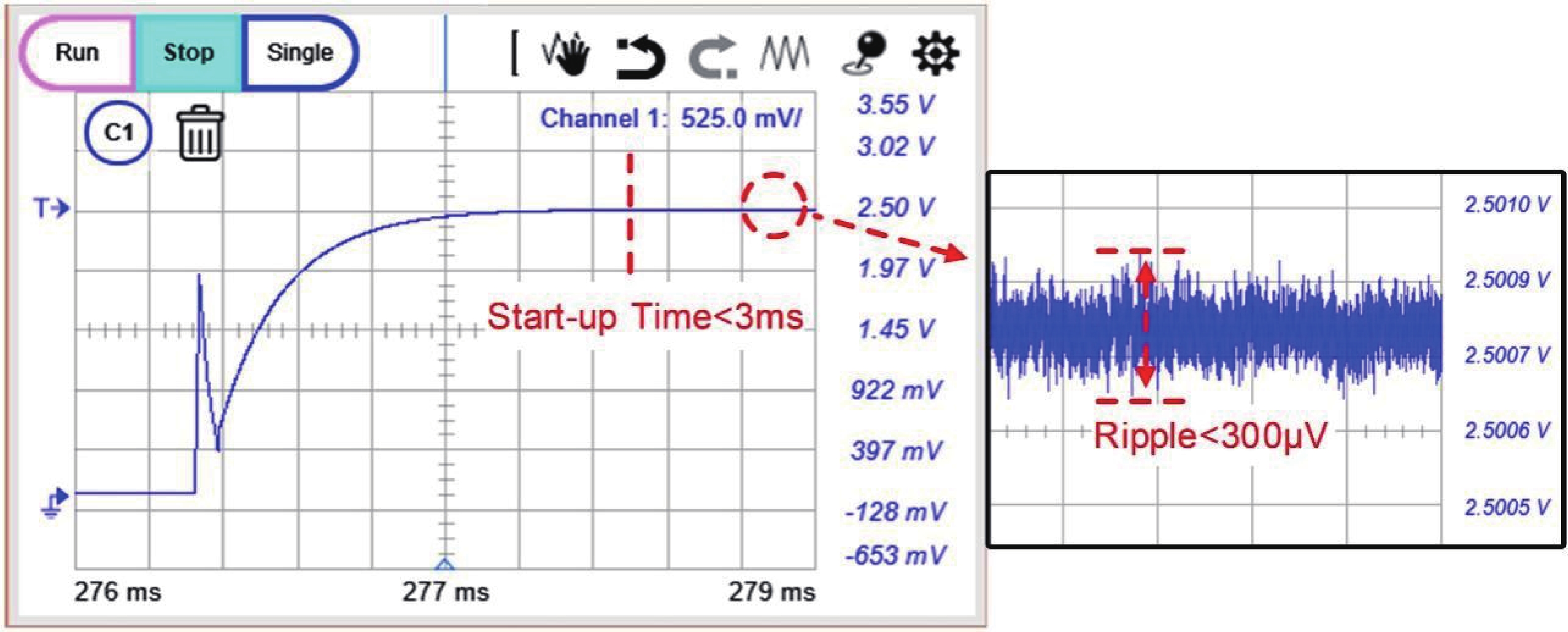
Table 1. Error sources in the proposed current-mode bandgap reference voltage.
| Type of error | Error proportion (%) | Design technique |
| Op-amp offset | 82.4 | Chopping technique |
| Mismatch of the current mirror |
7.7 | Curvature correction and trimming |
| Variation of the BJT | 7.3 | Curvature correction |
| Process variation and mismatch of the resistors | 2.6 | Trimming |
 DownLoad: CSV
Table 2. Performance summary and comparison.
| Parameters | This work | Ref. [11] JSSC’21 |
Ref. [14] TCAS-Ⅰ’22 |
Ref. [13] TCAS-Ⅰ’19 |
Ref. [16] JSSC’17 |
Ref. [6] TCAS-Ⅰ’24 |
|||
| Process (nm) | 180 | 180 | 130 | 180 | 350 | 65 | 180 | ||
| BGR type | Current-mode | Current- mode |
Current-mode | Voltage-mode | Voltage-mode | MOSFET | Current-mode | ||
| VREF (V) | 2.5 | 2.5 | 1.16 | 2.14 | 2.47 | 0.428 | 0.6 | ||
| Current (μA) | 84 | 84 | 120 | 409 | 94 | 16.25 | 69 | ||
| Temp. range (°C) | −40−125 | −40−125 | −40−150 | −25−125 | −45−125 | −40−125 | −45−125 | ||
| Trimming | Multi-point | Two-point (20 and 60°C) |
No | Two-point (−25 and 100°C) |
One-point | Two-point (−40 and 125°C) |
Multi-point | ||
| TC (ppm/°C) | 0.64 (min) 0.81 (avg) 0.98 (max) |
0.89 (min) 2.69 (avg) 5.88 (max) |
5.78 (min) 8.75 (avg) 13.5 (max) |
0.7 (min) 1.183 (avg) 1.557 (max) |
0.9 (min) 3.0 (avg) 7.52 (max) |
3.2 (min) 5.6 (avg) 9.8 (max) |
0.87 (min) 2.4 (avg) 2.95 (max) |
||
| LS (ppm/V) | 42 | 42 | 300 | 146 | 41 | 1000 | 30 | ||
| Max. load (μA) | 1000 | 1000 | NA | NA | 30 | NA | NA | ||
| Active area (mm2) | 0.548 | 0.548 | 0.08 | 0.256 | 0.0616 | 0.0104 | 0.088 | ||
| Samples | 20 | 38 | 7 | 6 | 10 | 50 | 10 | ||
DownLoad: CSV
| [1] |
Zhu G Q, Yang Y T, Zhang Q D. A 4.6-ppm/°C high-order curvature compensated bandgap reference for BMIC. IEEE Trans Circuits Syst II Express Briefs, 2019, 66(9), 1492 doi: 10.1109/TCSII.2018.2889808
|
| [2] |
Hunter B L, Matthews W E. A ± 3 ppm/°C single-trim switched capacitor bandgap reference for battery monitoring applications. IEEE Trans Circuits Syst I Regul Pap, 2017, 64(4), 777 doi: 10.1109/TCSI.2016.2621725
|
| [3] |
Boo J H, Cho K I, Kim H J, et al. A single-trim switched capacitor CMOS bandgap reference with a 3σ inaccuracy of 0.02%, −0.12% for battery-monitoring applications. IEEE J Solid State Circuits, 2021, 56(4), 1197 doi: 10.1109/JSSC.2020.3044165
|
| [4] |
Ma Y L, Bai C F, Wang Y, et al. A low noise CMOS bandgap voltage reference using chopper stabilization technique. 2020 IEEE 5th International Conference on Integrated Circuits and Microsystems (ICICM), 2020, 184 doi: 10.1109/ICICM50929.2020.9292198
|
| [5] |
Duan Q, Roh J. A 1.2-V 4.2-ppm/°C high-order curvature-compensated CMOS bandgap reference. IEEE Trans Circuits Syst I Regul Pap, 2015, 62(3), 662 doi: 10.1109/TCSI.2014.2374832
|
| [6] |
Ge G, Zhang C, Hoogzaad G, et al. A single-trim CMOS bandgap reference with a 3σ inaccuracy of ±0.15% from –40°C to 125°C. 2010 IEEE International Solid-State Circuits Conference-(ISSCC), 2010, 46(11), 2693 doi: 10.1109/JSSC.2011.2165235
|
| [7] |
Zhou Z K, Shi Y, Huang Z, et al. A 1.6-V 25-μA 5-ppm/°C curvature-compensated bandgap reference. IEEE Trans Circuits Syst I Regul Pap, 2012, 59(4), 677 doi: 10.1109/TCSI.2011.2169732
|
| [8] |
Maderbacher G, Marsili S, Motz M, et al. 5.8 A digitally assisted single-point-calibration CMOS bandgap voltage reference with a 3σ inaccuracy of ±0.08% for fuel-gauge applications. 2015 IEEE International Solid-State Circuits Conference-(ISSCC) Digest of Technical Papers, 2015, 1 doi: 10.1109/ISSCC.2015.7062946
|
| [9] |
Sheng J G, Chen Z L, Shi B X. A 1V supply area effective CMOS Bandgap reference. 2003 5th International Conference on ASIC Proceedings, 2003, 619 doi: 10.1109/ICASIC.2003.1277625
|
| [10] |
Chen H M, Lee C C, Jheng S H, et al. A sub-1 ppm/°C precision bandgap reference with adjusted-temperature-curvature compensation. IEEE Trans Circuits Syst I Regul Pap, 2017, 64(6), 1308 doi: 10.1109/TCSI.2017.2658186
|
| [11] |
Chen K, Petruzzi L, Hulfachor R, et al. A 1.16-V 5.8-to-13.5-ppm/°C curvature-compensated CMOS bandgap reference circuit with a shared offset-cancellation method for internal amplifiers. IEEE J Solid State Circuits, 2021, 56(1), 267 doi: 10.1109/JSSC.2020.3033467
|
| [12] |
Meijer G C M, Schmale P C, Van Zalinge K. A new curvature-corrected bandgap reference. IEEE J Solid State Circuits, 1982, 17(6), 1139 doi: 10.1109/JSSC.1982.1051872
|
| [13] |
Liu L X, Liao X F, Mu J C. A 3.6 μVrms noise, 3 ppm/°C TC bandgap reference with offset/noise suppression and five-piece linear compensation. IEEE Trans Circuits Syst I Regul Pap, 2019, 66(10), 3786 doi: 10.1109/TCSI.2019.2922652
|
| [14] |
Huang S L, Li M D, Li H, et al. A sub-1 ppm/°C bandgap voltage reference with high-order temperature compensation in 0.18-μm CMOS process. IEEE Trans Circuits Syst I Regul Pap, 2022, 69(4), 1408 doi: 10.1109/TCSI.2021.3139908
|
| [15] |
Liu N Q, Geiger R L, Chen D G. Sub-ppm/°C bandgap references with natural basis expansion for curvature cancellation. IEEE Trans Circuits Syst I Regul Pap, 2021, 68(9), 3551 doi: 10.1109/TCSI.2021.3096166
|
| [16] |
Jiang J Z, Shu W, Chang J S. A 5.6 ppm/°C temperature coefficient, 87-dB PSRR, sub-1-V voltage reference in 65-nm CMOS exploiting the zero-temperature-coefficient point. IEEE J Solid State Circuits, 2017, 52(3), 623 doi: 10.1109/JSSC.2016.2627544
|
| [17] |
Zhou Z K, Shi Y, Wang Y, et al. A resistorless high-precision compensated CMOS bandgap voltage reference. IEEE Trans Circuits Syst I Regul Pap, 2019, 66(1), 428 doi: 10.1109/TCSI.2018.2857821
|
| [18] |
Wang R C, Lu W G, Zhao M, et al. A sub-1ppm/°C current-mode CMOS bandgap reference with piecewise curvature compensation. IEEE Trans Circuits Syst I Regul Pap, 2018, 65(3), 904 doi: 10.1109/TCSI.2017.2771801
|
| [19] |
Ma B, Yu F Q. A novel 1.2–V 4.5-ppm/°C curvature-compensated CMOS bandgap reference. IEEE Trans Circuits Syst I Regul Pap, 2014, 61(4), 1026 doi: 10.1109/TCSI.2013.2286032
|
| [20] |
Liao X F, Zhang Y X, Zhang S H, et al. A 3.0 μ vrms, 2.4 ppm/°C BGR with feedback coefficient enhancement and bowl-shaped curvature compensation. IEEE Trans Circuits Syst I Regul Pap, 2024, 71(5), 2424 doi: 10.1109/TCSI.2024.3373788
|


Article views: 2517 Times PDF downloads: 427 Times Cited by: 0 Times
Received: 31 December 2024 Revised: 25 March 2025 Online: Accepted Manuscript: 30 April 2025Uncorrected proof: 15 May 2025Published: 05 June 2025
| Citation: |
Jing Wang, Feixiang Zhang, Zhiyuan He, Hui Zhang, Lin Cheng. A 2.69 ppm/°C bandgap reference with 42 ppm/V line sensitivity for battery management system[J]. Journal of Semiconductors, 2025, 46(6): 062203. doi: 10.1088/1674-4926/24120045
****
J Wang, F X Zhang, Z Y He, H Zhang, and L Cheng, A 2.69 ppm/°C bandgap reference with 42 ppm/V line sensitivity for battery management system[J]. J. Semicond., 2025, 46(6), 062203 doi: 10.1088/1674-4926/24120045

|
 Jing Wang received the B.Eng. degree from Sichuan University, Chengdu, China, in 2011. Then, she received the M.Sc. degree in 2012 and the Ph.D. degree in 2017 from Waseda University, Fukuoka, Japan, respectively. From 2017 to 2019, she was a post doctor in Waseda University, Japan. She is currently an associate researcher at the University of Science and Technology of China. Her research focuses on the design of high-precision, low-power analog front-end (AFE) circuits
 Lin Cheng received the B.Eng. degree from Hefei University of Technology, Hefei, China, in 2008, the M.Sc. degree from Fudan University, Shanghai, China, in 2011, and the Ph.D. degree from Hong Kong University of Science and Technology (HKUST), Hong Kong, in 2016. In 2018, he joined the School of Microelectronics, University of Science and Technology of China, Hefei, where he is currently a Professor. He was a Post-doctoral Research Associate at the Department of Electronic and Computer Engineering, HKUST, from 2016 to 2018, and was an Intern Analog Design Engineer with Broadcom Limited, San Jose, CA, USA, from 2015 to 2016. His current research interests include power management and mixed-signal integrated circuits and systems, wireless power transfer circuits and systems, switched-inductor power converters, and automotive ICs. Dr. Cheng is serving as a member of the ISSCC Technical Committee and the Chair of the IEEE ICTA 2024 Technical Committee. He was a recipient of the IEEE Solid-State Circuits Society Pre-Doctoral Achievement Award from 2014 to 2015, the Hong Kong Institution of Science 2018 Young Scientist Awards (Honorable Mention), and the Best Design Award from the IEEE ASP-DAC University Design Contest in 2020
| [1] |
Zhu G Q, Yang Y T, Zhang Q D. A 4.6-ppm/°C high-order curvature compensated bandgap reference for BMIC. IEEE Trans Circuits Syst II Express Briefs, 2019, 66(9), 1492 doi: 10.1109/TCSII.2018.2889808
|
| [2] |
Hunter B L, Matthews W E. A ± 3 ppm/°C single-trim switched capacitor bandgap reference for battery monitoring applications. IEEE Trans Circuits Syst I Regul Pap, 2017, 64(4), 777 doi: 10.1109/TCSI.2016.2621725
|
| [3] |
Boo J H, Cho K I, Kim H J, et al. A single-trim switched capacitor CMOS bandgap reference with a 3σ inaccuracy of 0.02%, −0.12% for battery-monitoring applications. IEEE J Solid State Circuits, 2021, 56(4), 1197 doi: 10.1109/JSSC.2020.3044165
|
| [4] |
Ma Y L, Bai C F, Wang Y, et al. A low noise CMOS bandgap voltage reference using chopper stabilization technique. 2020 IEEE 5th International Conference on Integrated Circuits and Microsystems (ICICM), 2020, 184 doi: 10.1109/ICICM50929.2020.9292198
|
| [5] |
Duan Q, Roh J. A 1.2-V 4.2-ppm/°C high-order curvature-compensated CMOS bandgap reference. IEEE Trans Circuits Syst I Regul Pap, 2015, 62(3), 662 doi: 10.1109/TCSI.2014.2374832
|
| [6] |
Ge G, Zhang C, Hoogzaad G, et al. A single-trim CMOS bandgap reference with a 3σ inaccuracy of ±0.15% from –40°C to 125°C. 2010 IEEE International Solid-State Circuits Conference-(ISSCC), 2010, 46(11), 2693 doi: 10.1109/JSSC.2011.2165235
|
| [7] |
Zhou Z K, Shi Y, Huang Z, et al. A 1.6-V 25-μA 5-ppm/°C curvature-compensated bandgap reference. IEEE Trans Circuits Syst I Regul Pap, 2012, 59(4), 677 doi: 10.1109/TCSI.2011.2169732
|
| [8] |
Maderbacher G, Marsili S, Motz M, et al. 5.8 A digitally assisted single-point-calibration CMOS bandgap voltage reference with a 3σ inaccuracy of ±0.08% for fuel-gauge applications. 2015 IEEE International Solid-State Circuits Conference-(ISSCC) Digest of Technical Papers, 2015, 1 doi: 10.1109/ISSCC.2015.7062946
|
| [9] |
Sheng J G, Chen Z L, Shi B X. A 1V supply area effective CMOS Bandgap reference. 2003 5th International Conference on ASIC Proceedings, 2003, 619 doi: 10.1109/ICASIC.2003.1277625
|
| [10] |
Chen H M, Lee C C, Jheng S H, et al. A sub-1 ppm/°C precision bandgap reference with adjusted-temperature-curvature compensation. IEEE Trans Circuits Syst I Regul Pap, 2017, 64(6), 1308 doi: 10.1109/TCSI.2017.2658186
|
| [11] |
Chen K, Petruzzi L, Hulfachor R, et al. A 1.16-V 5.8-to-13.5-ppm/°C curvature-compensated CMOS bandgap reference circuit with a shared offset-cancellation method for internal amplifiers. IEEE J Solid State Circuits, 2021, 56(1), 267 doi: 10.1109/JSSC.2020.3033467
|
| [12] |
Meijer G C M, Schmale P C, Van Zalinge K. A new curvature-corrected bandgap reference. IEEE J Solid State Circuits, 1982, 17(6), 1139 doi: 10.1109/JSSC.1982.1051872
|
| [13] |
Liu L X, Liao X F, Mu J C. A 3.6 μVrms noise, 3 ppm/°C TC bandgap reference with offset/noise suppression and five-piece linear compensation. IEEE Trans Circuits Syst I Regul Pap, 2019, 66(10), 3786 doi: 10.1109/TCSI.2019.2922652
|
| [14] |
Huang S L, Li M D, Li H, et al. A sub-1 ppm/°C bandgap voltage reference with high-order temperature compensation in 0.18-μm CMOS process. IEEE Trans Circuits Syst I Regul Pap, 2022, 69(4), 1408 doi: 10.1109/TCSI.2021.3139908
|
| [15] |
Liu N Q, Geiger R L, Chen D G. Sub-ppm/°C bandgap references with natural basis expansion for curvature cancellation. IEEE Trans Circuits Syst I Regul Pap, 2021, 68(9), 3551 doi: 10.1109/TCSI.2021.3096166
|
| [16] |
Jiang J Z, Shu W, Chang J S. A 5.6 ppm/°C temperature coefficient, 87-dB PSRR, sub-1-V voltage reference in 65-nm CMOS exploiting the zero-temperature-coefficient point. IEEE J Solid State Circuits, 2017, 52(3), 623 doi: 10.1109/JSSC.2016.2627544
|
| [17] |
Zhou Z K, Shi Y, Wang Y, et al. A resistorless high-precision compensated CMOS bandgap voltage reference. IEEE Trans Circuits Syst I Regul Pap, 2019, 66(1), 428 doi: 10.1109/TCSI.2018.2857821
|
| [18] |
Wang R C, Lu W G, Zhao M, et al. A sub-1ppm/°C current-mode CMOS bandgap reference with piecewise curvature compensation. IEEE Trans Circuits Syst I Regul Pap, 2018, 65(3), 904 doi: 10.1109/TCSI.2017.2771801
|
| [19] |
Ma B, Yu F Q. A novel 1.2–V 4.5-ppm/°C curvature-compensated CMOS bandgap reference. IEEE Trans Circuits Syst I Regul Pap, 2014, 61(4), 1026 doi: 10.1109/TCSI.2013.2286032
|
| [20] |
Liao X F, Zhang Y X, Zhang S H, et al. A 3.0 μ vrms, 2.4 ppm/°C BGR with feedback coefficient enhancement and bowl-shaped curvature compensation. IEEE Trans Circuits Syst I Regul Pap, 2024, 71(5), 2424 doi: 10.1109/TCSI.2024.3373788
|

 WeChat ID
Journal of Semiconductors © 2017 All Rights Reserved 京ICP备05085259号-2