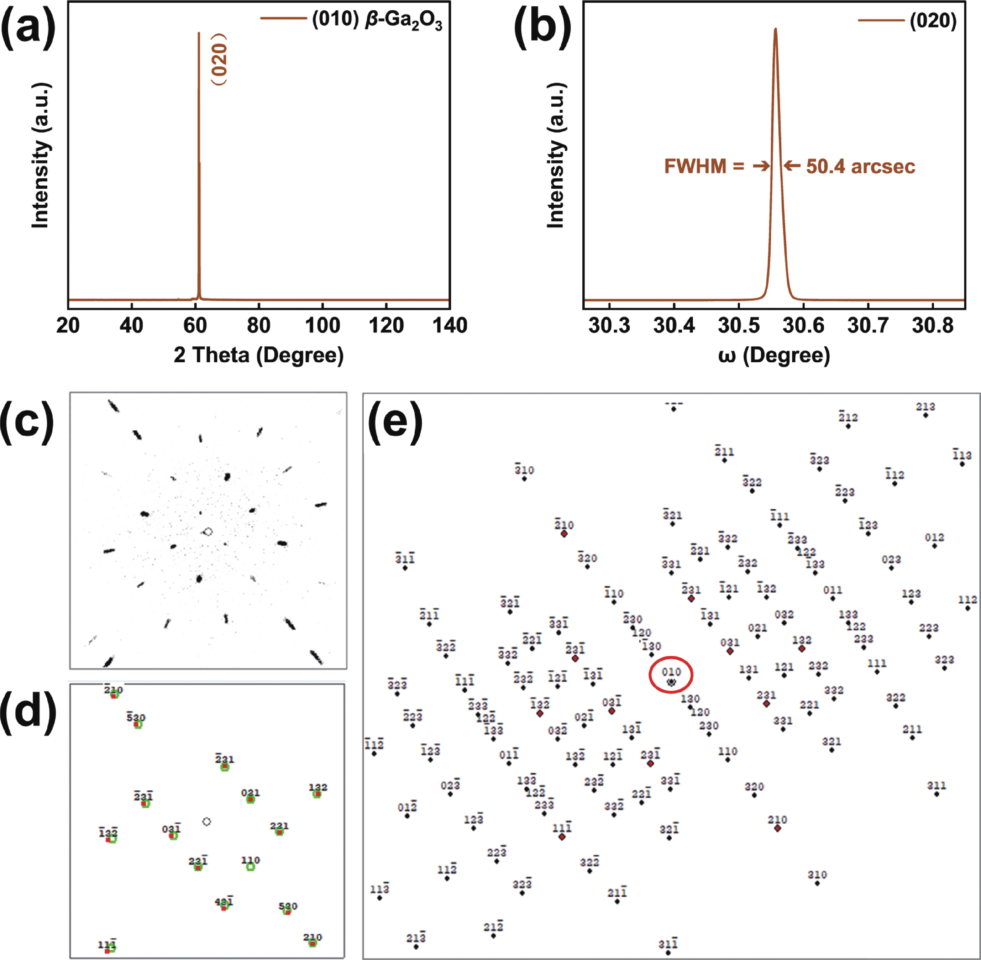
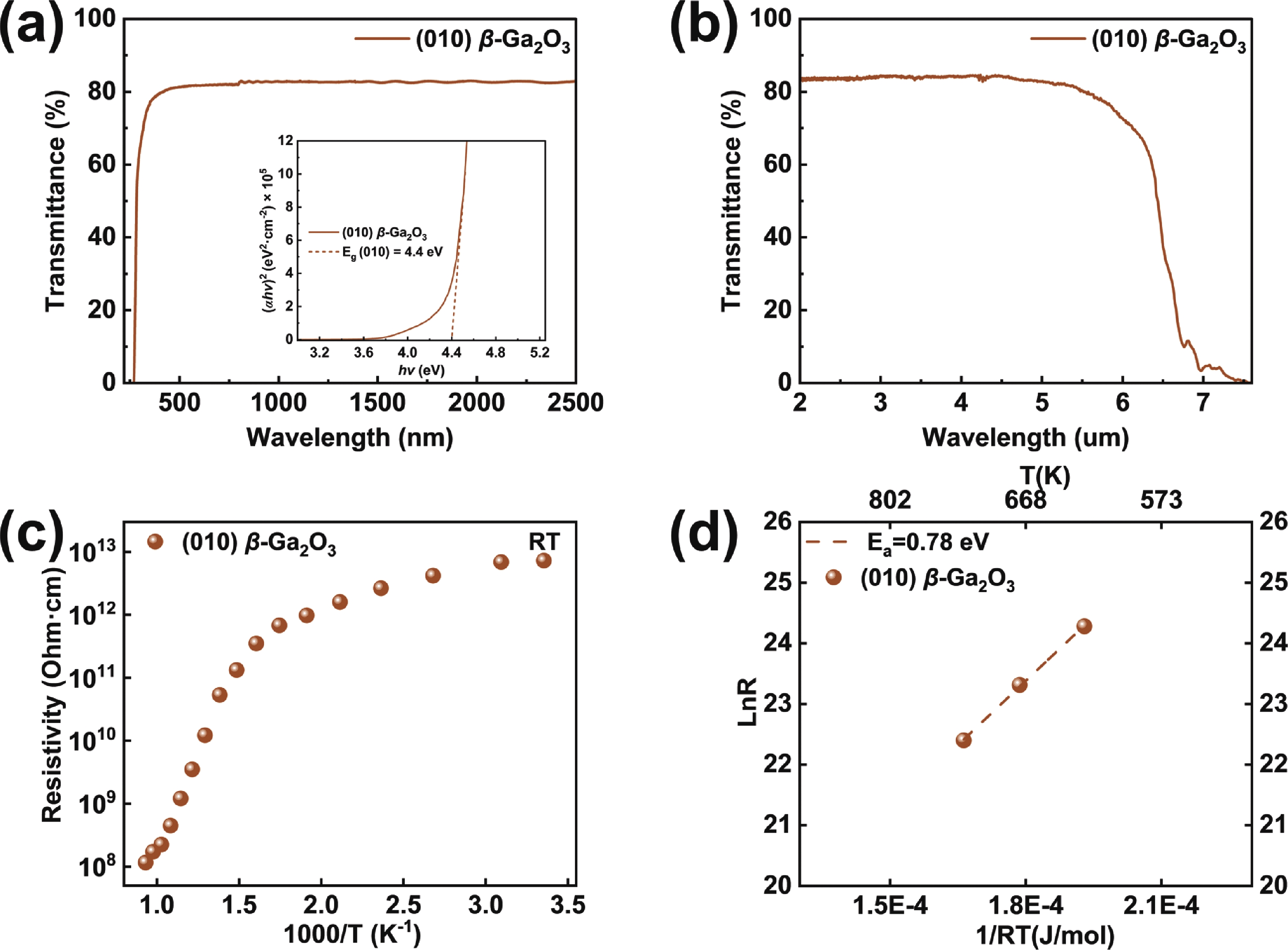
J. Semicond. >  In Press

ARTICLES

2-inch diameter (010) principal-face β-Ga2O3 single crystals grown by EFG method

Xuyang Dong1, Wenxiang Mu1, , Pei Wang1, Yue Dong1, Hao Zhao1, Boyang Chen1, Zhitai Jia1, 2, and Xutang Tao1

+ Author Affiliations

 Corresponding author: Wenxiang Mu, mwx@sdu.edu.cn; Zhitai Jia, z.jia@sdu.edu.cn

DOI: 10.1088/1674-4926/24110029CSTR: 32376.14.1674-4926.24110029

PDF

Turn off MathJax

Abstract: The (010)-oriented substrates of β-Ga2O3 are endowed with the maximum thermal conductivity and fastest homoepitaxial rate, which is the preferred substrate direction for high-power devices. However, the size of (010) plane wafer is critically limited by die in the commercial edge-defined film-fed growth (EFG) method. It is difficult to grow the β-Ga2O3 crystal with (010) principal face due to the (100) and (001) are cleavage planes. Here, the 2-inch diameter (010) principal-face β-Ga2O3 single crystal is successfully designed and grown by improved EFG method. Unlike previous reported techniques, the single crystals are pulled with [001] direction, and in this way the (010) wafers can be obtained from the principal face. In our experiments, tree-like defects (TLDs) in (010) principal-face bulk crystals are easy to generate. The relationship between stability of growth interface and origin of TLDs are thoroughly discussed. The TLDs are successfully eliminated by optimizing growth conditions. The high crystalline quality of (010)-oriented substrates are comprehensive demonstrated by full width at half maximum (FWHM) with 50.4 arcsec, consistent orientation arrangement of (010) plane, respectively. This work shows that the (010)-oriented substrates can be obtained by EFG method, predicting the commercial prospects of large-scale (010)-oriented β-Ga2O3 substrates.

Key words: β-Ga2O3EFG(010) principal-face single crystal


[1]
Zhang J C, Dong P F, Dang K, et al. Ultra-wide bandgap semiconductor Ga2O3 power diodes. Nat Commun, 2022, 13, 3900 doi: 10.1038/s41467-022-31664-y
[2]
Tsao J Y, Chowdhury S, Hollis M A, et al. Ultrawide-bandgap semiconductors: Research opportunities and challenges. Adv Elect Materials, 2018, 4(1), 1600501 doi: 10.1002/aelm.201600501
[3]
Pearton S J, Yang J C, Cary P H, et al. A review of Ga2O3 materials, processing, and devices. Appl Phys Rev, 2018, 5(1), 011301 doi: 10.1063/1.5006941
[4]
Heinselman K N, Haven D, Zakutayev A, et al. Projected cost of gallium oxide wafers from edge-defined film-fed crystal growth. Cryst Growth Des, 2022, 22(8), 4854 doi: 10.1021/acs.cgd.2c00340
[5]
Lu X, Deng Y X, Pei Y L, et al. Recent advances in NiO/Ga2O3 heterojunctions for power electronics. J Semicond, 2023, 44(6), 061802 doi: 10.1088/1674-4926/44/6/061802
[6]
Xu G W, Wu F H, Liu Q, et al. Vertical β-Ga2O3 power electronics. J Semicond, 2023, 44(7), 070301 doi: 10.1088/1674-4926/44/7/070301
[7]
Wei J S, Bu Y Z, Sai Q L, et al. Effect of high-temperature remelting on the properties of Sn-doped β-Ga2O3 crystal grown using the EFG method. CrystEngComm, 2023, 25(30), 4317 doi: 10.1039/D3CE00415E
[8]
Mastro M A, Kuramata A, Calkins J, et al. Perspective: Opportunities and future directions for Ga2O3. ECS J Solid State Sci Technol, 2017, 6(5), P356 doi: 10.1149/2.0031707jss
[9]
Aida H, Nishiguchi K, Takeda H, et al. Growth of β-Ga2O3 single crystals by the edge-defined, film fed growth method. Jjap, 2008, 47(11R), 8506 doi: 10.1143/JJAP.47.8506
[10]
Ohba E, Kobayashi T, Taishi T, et al. Growth of (100), (010) and (001) β-Ga2O3 single crystals by vertical Bridgman method. J Cryst Growth, 2021, 556, 125990 doi: 10.1016/j.jcrysgro.2020.125990
[11]
Hoshikawa K, Ohba E, Kobayashi T, et al. Growth of β-Ga2O3 single crystals using vertical Bridgman method in ambient air. J Cryst Growth, 2016, 447, 36 doi: 10.1016/j.jcrysgro.2016.04.022
[12]
Galazka Z. Growth of bulk β-Ga2O3 single crystals by the Czochralski method. 2022, 131(3), 0311, 03
[13]
Chen B Y, Mu W X, Liu Y Y, et al. Growth and characterization of the β-Ga2O3 (011) plane without line-shaped defects. CrystEngComm, 2023, 25(16), 2404 doi: 10.1039/D3CE00052D
[14]
Li P K, Han X L, Chen D Y, et al. Controllability of β-Ga2O3 single crystal conductivity by V doping. CrystEngComm, 2022, 24(31), 5588 doi: 10.1039/D2CE00418F
[15]
Zhang Q Y, Li N, Zhang T, et al. Enhanced gain and detectivity of unipolar barrier solar blind avalanche photodetector via lattice and band engineering. Nat Commun, 2023, 14(1), 418 doi: 10.1038/s41467-023-36117-8
[16]
Guo D, Guo Q, Chen Z, et al. Review of Ga2O3-based optoelectronic devices. Mater Today Phys, 2019, 11, 100157 doi: 10.1016/j.mtphys.2019.100157
[17]
Song Y W, Bhattacharyya A, Karim A, et al. Ultra-wide band gap Ga2O3-on-SiC MOSFETs. ACS Appl Mater Interfaces, 2023, 15(5), 7137 doi: 10.1021/acsami.2c21048
[18]
Singh M, Casbon M A, Uren M J, et al. Pulsed large signal RF performance of field-plated Ga2O3 MOSFETs. IEEE Electron Device Lett, 2018, 39(10), 1572 doi: 10.1109/LED.2018.2865832
[19]
Moser N, Liddy K, Islam A, et al. Toward high voltage radio frequency devices in β-Ga2O3. Appl Phys Lett, 2020, 117(24), 242101 doi: 10.1063/5.0031482
[20]
Mu W X, Jia Z T, Cittadino G, et al. Ti-doped β-Ga2O3: A promising material for ultrafast and tunable lasers. Cryst Growth Des, 2018, 18(5), 3037 doi: 10.1021/acs.cgd.8b00182
[21]
Zhang Y H, Xing F. Anisotropic optical and electric properties of β-gallium oxide. J Semicond, 2023, 44(7), 071801 doi: 10.1088/1674-4926/44/7/071801
[22]
Lovejoy T C, Yitamben E N, Shamir N, et al. Surface morphology and electronic structure of bulk single crystal β-Ga2O3 (100). Appl Phys Lett, 2009, 94(8), 1906
[23]
Bermudez V M. The structure of low-index surfaces of β-Ga2O3. Chem Phys, 2006, 323(2/3), 193
[24]
Meng L Y, Yu D S, Huang H L, et al. MOCVD Growth of β-Ga2O3 on (001) Ga2O3 Substrates. Cryst Growth Des, 2024, 24(9), 3737 doi: 10.1021/acs.cgd.4c00060
[25]
Nandi A, Cherns D, Sanyal I, et al. Epitaxial growth of (-201) β-Ga2O3 on (001) diamond substrates. Cryst Growth Des, 2023, 23(11), 8290 doi: 10.1021/acs.cgd.3c00972
[26]
Bu Y Z, Sai Q L, Qi H J. Stability of interfacial thermal balance in thick β-Ga2O3 crystal growth by EFG. J Cryst Growth, 2023, 612, 127194 doi: 10.1016/j.jcrysgro.2023.127194
[27]
Mu W X, Jia Z T, Yin Y R, et al. Solid-liquid interface optimization and properties of ultra-wide bandgap β-Ga2O3 grown by Czochralski and EFG methods. CrystEngComm, 2019, 21(17), 2762 doi: 10.1039/C8CE02189A
[28]
Tang X, Liu B T, Yu Y, et al. Numerical analysis of difficulties of growing large-size bulk β-Ga2O3 single crystals with the czochralski method. Crystals, 2021, 11(1), 25
[29]
Kuramata A, Koshi K, Watanabe S, et al. High-quality β-Ga2O3 single crystals grown by edge-defined film-fed growth. Jpn J Appl Phys, 2016, 55(12), 1202A2 doi: 10.7567/JJAP.55.1202A2
[30]
Hou T, Zhang W Y, Mu W X, et al. The anisotropy dependence of deformation mechanism of cleavage planes in β-Ga2O3 single crystal. Mater Sci Semicond Process, 2023, 158, 107357 doi: 10.1016/j.mssp.2023.107357
[31]
Ge M, Li Y, Zhu Y H, et al. An improved design for e-mode AlGaN/GaN HEMT with gate stack β-Ga2O3/p-GaN structure. J Appl Phys, 2021, 130(3), 035703 doi: 10.1063/5.0051274
[32]
Yao Y Z, Hirano K, Sugawara Y, et al. Observation of dislocations in thick β-Ga2O3 single-crystal substrates using Borrmann effect synchrotron X-ray topography. Apl Materials, 2022, 10(5), 051101 doi: 10.1063/5.0088701
[33]
Ueda O, Kasu M, Yamaguchi H. Structural characterization of defects in EFG- and HVPE-grown β-Ga2O3 crystals. Jpn J Appl Phys, 2022, 61(5), 050101 doi: 10.35848/1347-4065/ac4b6b
[34]
Yao Y Z, Tsusaka Y, Hirano K, et al. Three-dimensional distribution and propagation of dislocations in β-Ga2O3 revealed by Borrmann effect X-ray topography. J Appl Phys, 2023, 134(15), 155104 doi: 10.1063/5.0169526
[35]
Ma X C, Xu R, Xu J F, et al. In-plane crystalline anisotropy of bulk β-Ga2O3. J Appl Cryst, 2021, 54(4), 1153 doi: 10.1107/S1600576721006427
[36]
Wang M G, Mu S, Speck J S, et al. First-principles study of twin boundaries and stacking faults in β-Ga2O3. Adv Materials Inter, 2025, 12(2), 2300318 doi: 10.1002/admi.202300318
[37]
Haven D, Moutinho H, Mangum J S, et al. Multimodal microscopy of extended defects in β-Ga2O3 (010) EFG crystals. AIP Advances, 2023, 13(7), 075122 doi: 10.1063/5.0158904
[38]
Gu Y, Wang W W, Li Y J, et al. Designable ultra-smooth ultra-thin solid-electrolyte interphases of three alkali metal anodes. Nat Commun, 2018, 9(1), 1339 doi: 10.1038/s41467-018-03466-8
[39]
Lee B, Paek E, Mitlin D, et al. Sodium metal anodes: emerging solutions to dendrite growth. Chem Rev, 2019, 119(8), 5416 doi: 10.1021/acs.chemrev.8b00642
[40]
Li C Z, Yuan Q, Ni B, et al. Dendritic defect-rich palladium-copper-cobalt nanoalloys as robust multifunctional non-platinum electrocatalysts for fuel cells. Nat Commun, 2018, 9(1), 3702 doi: 10.1038/s41467-018-06043-1
[41]
Liu Y J, Li S J, Wang H L, et al. Microstructure, defects and mechanical behavior of beta-type titanium porous structures manufactured by electron beam melting and selective laser melting. Acta Mater, 2016, 113, 56 doi: 10.1016/j.actamat.2016.04.029
[42]
Glicksman M E, Lupulescu A O. Dendritic crystal growth in pure materials. J Cryst Growth, 2004, 264(4), 541 doi: 10.1016/j.jcrysgro.2003.12.034
[43]
Gránásy L, Pusztai T, Börzsönyi T, et al. A general mechanism of polycrystalline growth. Nature Mater, 2004, 3(9), 645 doi: 10.1038/nmat1190
[44]
Dong X Y, Yu S J, Mu W X, et al. Solar-blind photodetectors prepared using semi-insulating Co: β-Ga2O3 single crystals that are stable over a wide temperature range. J Mater Chem C, 2023, 11(26), 8919 doi: 10.1039/D3TC00906H
Fig. 1.  (Color online) (a) Schematic diagram of (010) principal-face β-Ga2O3 bulk crystals grown by EFG method. (b) (010) principal-face macro-morphology image of TLDs, showing obvious branching tendency of evolution process with (001) pulling direction from right to left. (c) Enlarged-morphology image of red rectangular block from (b). (d) Micro-morphology image of TLDs of yellow rectangular block in (b). (e) 2-inch diameter (010) principal-face non-TLDs β-Ga2O3 single crystal.

Fig. 2.  (Color online) (a) SEM image of (010) principal-face β-Ga2O3 bulk crystals growth cross section at early pulling stage, the bright region with branches is cross-sectional TLDs, enlarged images of (b)−(f) are different location in (a) marked by yellow rectangular block, and the location of (b) is termination point of TLDs, exhibiting destructive effect for crystalline structure of β-Ga2O3 bulk crystals. (g) SEM image of growth cross section at later growth stage of the same bulk crystal, the bright region is cross-sectional TLDs, showing the worse surface morphology than early stage in (a), enlarged images of (h) and (i) are also marked in (g), indicating severe deteriorating scene of TLDs.

Fig. 3.  (Color online) (a) XRD pattern and (b) X-ray rocking curve of (010)-oriented substrate from (010) principal-face β-Ga2O3 single crystal. (c) Laue diffraction image, (d) indexation of Laue spots, and (e) identification of (010)-oriented crystallographic plane, manifesting great symmetry and consistency.

Fig. 4.  (Color online) (a) UV−VIS−NIR transmittance spectra of (010)-oriented β-Ga2O3, the inset is optical bandgap with 4.4 eV of (010) plane. (b) MWIR transmittance spectra of (010)-oriented β-Ga2O3, showing wide transmission range from UV to MWIR band. (c) Temperature-dependent resistivity of (010)-oriented β-Ga2O3. (d) Fe acceptor activation energy with 0.78 eV was fitted with Arrhenius equation.

[1]
Zhang J C, Dong P F, Dang K, et al. Ultra-wide bandgap semiconductor Ga2O3 power diodes. Nat Commun, 2022, 13, 3900 doi: 10.1038/s41467-022-31664-y
[2]
Tsao J Y, Chowdhury S, Hollis M A, et al. Ultrawide-bandgap semiconductors: Research opportunities and challenges. Adv Elect Materials, 2018, 4(1), 1600501 doi: 10.1002/aelm.201600501
[3]
Pearton S J, Yang J C, Cary P H, et al. A review of Ga2O3 materials, processing, and devices. Appl Phys Rev, 2018, 5(1), 011301 doi: 10.1063/1.5006941
[4]
Heinselman K N, Haven D, Zakutayev A, et al. Projected cost of gallium oxide wafers from edge-defined film-fed crystal growth. Cryst Growth Des, 2022, 22(8), 4854 doi: 10.1021/acs.cgd.2c00340
[5]
Lu X, Deng Y X, Pei Y L, et al. Recent advances in NiO/Ga2O3 heterojunctions for power electronics. J Semicond, 2023, 44(6), 061802 doi: 10.1088/1674-4926/44/6/061802
[6]
Xu G W, Wu F H, Liu Q, et al. Vertical β-Ga2O3 power electronics. J Semicond, 2023, 44(7), 070301 doi: 10.1088/1674-4926/44/7/070301
[7]
Wei J S, Bu Y Z, Sai Q L, et al. Effect of high-temperature remelting on the properties of Sn-doped β-Ga2O3 crystal grown using the EFG method. CrystEngComm, 2023, 25(30), 4317 doi: 10.1039/D3CE00415E
[8]
Mastro M A, Kuramata A, Calkins J, et al. Perspective: Opportunities and future directions for Ga2O3. ECS J Solid State Sci Technol, 2017, 6(5), P356 doi: 10.1149/2.0031707jss
[9]
Aida H, Nishiguchi K, Takeda H, et al. Growth of β-Ga2O3 single crystals by the edge-defined, film fed growth method. Jjap, 2008, 47(11R), 8506 doi: 10.1143/JJAP.47.8506
[10]
Ohba E, Kobayashi T, Taishi T, et al. Growth of (100), (010) and (001) β-Ga2O3 single crystals by vertical Bridgman method. J Cryst Growth, 2021, 556, 125990 doi: 10.1016/j.jcrysgro.2020.125990
[11]
Hoshikawa K, Ohba E, Kobayashi T, et al. Growth of β-Ga2O3 single crystals using vertical Bridgman method in ambient air. J Cryst Growth, 2016, 447, 36 doi: 10.1016/j.jcrysgro.2016.04.022
[12]
Galazka Z. Growth of bulk β-Ga2O3 single crystals by the Czochralski method. 2022, 131(3), 0311, 03
[13]
Chen B Y, Mu W X, Liu Y Y, et al. Growth and characterization of the β-Ga2O3 (011) plane without line-shaped defects. CrystEngComm, 2023, 25(16), 2404 doi: 10.1039/D3CE00052D
[14]
Li P K, Han X L, Chen D Y, et al. Controllability of β-Ga2O3 single crystal conductivity by V doping. CrystEngComm, 2022, 24(31), 5588 doi: 10.1039/D2CE00418F
[15]
Zhang Q Y, Li N, Zhang T, et al. Enhanced gain and detectivity of unipolar barrier solar blind avalanche photodetector via lattice and band engineering. Nat Commun, 2023, 14(1), 418 doi: 10.1038/s41467-023-36117-8
[16]
Guo D, Guo Q, Chen Z, et al. Review of Ga2O3-based optoelectronic devices. Mater Today Phys, 2019, 11, 100157 doi: 10.1016/j.mtphys.2019.100157
[17]
Song Y W, Bhattacharyya A, Karim A, et al. Ultra-wide band gap Ga2O3-on-SiC MOSFETs. ACS Appl Mater Interfaces, 2023, 15(5), 7137 doi: 10.1021/acsami.2c21048
[18]
Singh M, Casbon M A, Uren M J, et al. Pulsed large signal RF performance of field-plated Ga2O3 MOSFETs. IEEE Electron Device Lett, 2018, 39(10), 1572 doi: 10.1109/LED.2018.2865832
[19]
Moser N, Liddy K, Islam A, et al. Toward high voltage radio frequency devices in β-Ga2O3. Appl Phys Lett, 2020, 117(24), 242101 doi: 10.1063/5.0031482
[20]
Mu W X, Jia Z T, Cittadino G, et al. Ti-doped β-Ga2O3: A promising material for ultrafast and tunable lasers. Cryst Growth Des, 2018, 18(5), 3037 doi: 10.1021/acs.cgd.8b00182
[21]
Zhang Y H, Xing F. Anisotropic optical and electric properties of β-gallium oxide. J Semicond, 2023, 44(7), 071801 doi: 10.1088/1674-4926/44/7/071801
[22]
Lovejoy T C, Yitamben E N, Shamir N, et al. Surface morphology and electronic structure of bulk single crystal β-Ga2O3 (100). Appl Phys Lett, 2009, 94(8), 1906
[23]
Bermudez V M. The structure of low-index surfaces of β-Ga2O3. Chem Phys, 2006, 323(2/3), 193
[24]
Meng L Y, Yu D S, Huang H L, et al. MOCVD Growth of β-Ga2O3 on (001) Ga2O3 Substrates. Cryst Growth Des, 2024, 24(9), 3737 doi: 10.1021/acs.cgd.4c00060
[25]
Nandi A, Cherns D, Sanyal I, et al. Epitaxial growth of (-201) β-Ga2O3 on (001) diamond substrates. Cryst Growth Des, 2023, 23(11), 8290 doi: 10.1021/acs.cgd.3c00972
[26]
Bu Y Z, Sai Q L, Qi H J. Stability of interfacial thermal balance in thick β-Ga2O3 crystal growth by EFG. J Cryst Growth, 2023, 612, 127194 doi: 10.1016/j.jcrysgro.2023.127194
[27]
Mu W X, Jia Z T, Yin Y R, et al. Solid-liquid interface optimization and properties of ultra-wide bandgap β-Ga2O3 grown by Czochralski and EFG methods. CrystEngComm, 2019, 21(17), 2762 doi: 10.1039/C8CE02189A
[28]
Tang X, Liu B T, Yu Y, et al. Numerical analysis of difficulties of growing large-size bulk β-Ga2O3 single crystals with the czochralski method. Crystals, 2021, 11(1), 25
[29]
Kuramata A, Koshi K, Watanabe S, et al. High-quality β-Ga2O3 single crystals grown by edge-defined film-fed growth. Jpn J Appl Phys, 2016, 55(12), 1202A2 doi: 10.7567/JJAP.55.1202A2
[30]
Hou T, Zhang W Y, Mu W X, et al. The anisotropy dependence of deformation mechanism of cleavage planes in β-Ga2O3 single crystal. Mater Sci Semicond Process, 2023, 158, 107357 doi: 10.1016/j.mssp.2023.107357
[31]
Ge M, Li Y, Zhu Y H, et al. An improved design for e-mode AlGaN/GaN HEMT with gate stack β-Ga2O3/p-GaN structure. J Appl Phys, 2021, 130(3), 035703 doi: 10.1063/5.0051274
[32]
Yao Y Z, Hirano K, Sugawara Y, et al. Observation of dislocations in thick β-Ga2O3 single-crystal substrates using Borrmann effect synchrotron X-ray topography. Apl Materials, 2022, 10(5), 051101 doi: 10.1063/5.0088701
[33]
Ueda O, Kasu M, Yamaguchi H. Structural characterization of defects in EFG- and HVPE-grown β-Ga2O3 crystals. Jpn J Appl Phys, 2022, 61(5), 050101 doi: 10.35848/1347-4065/ac4b6b
[34]
Yao Y Z, Tsusaka Y, Hirano K, et al. Three-dimensional distribution and propagation of dislocations in β-Ga2O3 revealed by Borrmann effect X-ray topography. J Appl Phys, 2023, 134(15), 155104 doi: 10.1063/5.0169526
[35]
Ma X C, Xu R, Xu J F, et al. In-plane crystalline anisotropy of bulk β-Ga2O3. J Appl Cryst, 2021, 54(4), 1153 doi: 10.1107/S1600576721006427
[36]
Wang M G, Mu S, Speck J S, et al. First-principles study of twin boundaries and stacking faults in β-Ga2O3. Adv Materials Inter, 2025, 12(2), 2300318 doi: 10.1002/admi.202300318
[37]
Haven D, Moutinho H, Mangum J S, et al. Multimodal microscopy of extended defects in β-Ga2O3 (010) EFG crystals. AIP Advances, 2023, 13(7), 075122 doi: 10.1063/5.0158904
[38]
Gu Y, Wang W W, Li Y J, et al. Designable ultra-smooth ultra-thin solid-electrolyte interphases of three alkali metal anodes. Nat Commun, 2018, 9(1), 1339 doi: 10.1038/s41467-018-03466-8
[39]
Lee B, Paek E, Mitlin D, et al. Sodium metal anodes: emerging solutions to dendrite growth. Chem Rev, 2019, 119(8), 5416 doi: 10.1021/acs.chemrev.8b00642
[40]
Li C Z, Yuan Q, Ni B, et al. Dendritic defect-rich palladium-copper-cobalt nanoalloys as robust multifunctional non-platinum electrocatalysts for fuel cells. Nat Commun, 2018, 9(1), 3702 doi: 10.1038/s41467-018-06043-1
[41]
Liu Y J, Li S J, Wang H L, et al. Microstructure, defects and mechanical behavior of beta-type titanium porous structures manufactured by electron beam melting and selective laser melting. Acta Mater, 2016, 113, 56 doi: 10.1016/j.actamat.2016.04.029
[42]
Glicksman M E, Lupulescu A O. Dendritic crystal growth in pure materials. J Cryst Growth, 2004, 264(4), 541 doi: 10.1016/j.jcrysgro.2003.12.034
[43]
Gránásy L, Pusztai T, Börzsönyi T, et al. A general mechanism of polycrystalline growth. Nature Mater, 2004, 3(9), 645 doi: 10.1038/nmat1190
[44]
Dong X Y, Yu S J, Mu W X, et al. Solar-blind photodetectors prepared using semi-insulating Co: β-Ga2O3 single crystals that are stable over a wide temperature range. J Mater Chem C, 2023, 11(26), 8919 doi: 10.1039/D3TC00906H

24110029Supplementary Information.pdf

  • Search

    Advanced Search >>

    GET CITATION

    shu

    Export: BibTex EndNote

    Article Metrics

    Article views: 342 Times PDF downloads: 64 Times Cited by: 0 Times

    History

    Received: 21 December 2024 Revised: 23 January 2025 Online: Accepted Manuscript: 18 February 2025Uncorrected proof: 21 March 2025

    Catalog

      Email This Article

      User name:
      Email:*请输入正确邮箱
      Code:*验证码错误
      Xuyang Dong, Wenxiang Mu, Pei Wang, Yue Dong, Hao Zhao, Boyang Chen, Zhitai Jia, Xutang Tao. 2-inch diameter (010) principal-face β-Ga2O3 single crystals grown by EFG method[J]. Journal of Semiconductors, 2025, In Press. doi: 10.1088/1674-4926/24110029 ****X Y Dong, W X Mu, P Wang, Y Dong, H Zhao, B Y Chen, Z T Jia, and X T Tao, 2-inch diameter (010) principal-face β-Ga2O3 single crystals grown by EFG method[J]. J. Semicond., 2025, 46(6), 062501 doi: 10.1088/1674-4926/24110029
      Citation:
      Xuyang Dong, Wenxiang Mu, Pei Wang, Yue Dong, Hao Zhao, Boyang Chen, Zhitai Jia, Xutang Tao. 2-inch diameter (010) principal-face β-Ga2O3 single crystals grown by EFG method[J]. Journal of Semiconductors, 2025, In Press. doi: 10.1088/1674-4926/24110029 ****
      X Y Dong, W X Mu, P Wang, Y Dong, H Zhao, B Y Chen, Z T Jia, and X T Tao, 2-inch diameter (010) principal-face β-Ga2O3 single crystals grown by EFG method[J]. J. Semicond., 2025, 46(6), 062501 doi: 10.1088/1674-4926/24110029

      2-inch diameter (010) principal-face β-Ga2O3 single crystals grown by EFG method

      DOI: 10.1088/1674-4926/24110029
      CSTR: 32376.14.1674-4926.24110029
      More Information
      • Xuyang Dong got his BS degree from Nanjing Tech University in 2019. Now he is a PhD student at Shandong University under the supervision of Prof. Zhitai Jia. His research focuses on the crystal growth and investigation of properties of ultrawide-bandgap semiconductor material of β-Ga2O3
      • Wenxiang Mu got his BS degree in 2013 and PhD degree in 2018 at Shandong University. Now he is an associate professor at institute of novel semiconductors of Shandong University. His research interests include crystal growth, substrate processing, performance optimization and device design based on ultrawide-bandgap semiconductor material of β-Ga2O3
      • Zhitai Jia got his BS degree in 2003 and PhD degree in 2008 at Shandong University. Now he is a full professor at institute of novel semiconductors of Shandong University. His research focuses on the crystal growth, performance optimization and device design of oxide semiconductor and magneto-optic functional crystal
      • Corresponding author: mwx@sdu.edu.cnz.jia@sdu.edu.cn
      • Received Date: 2024-12-21
      • Revised Date: 2025-01-23
      • Available Online: 2025-02-18

      Catalog

        /

        DownLoad:  Full-Size Img  PowerPoint
        Return
        Return