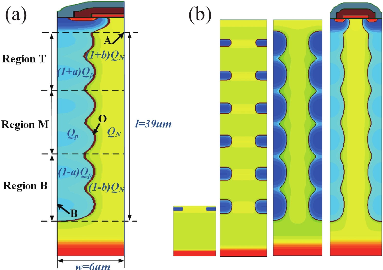
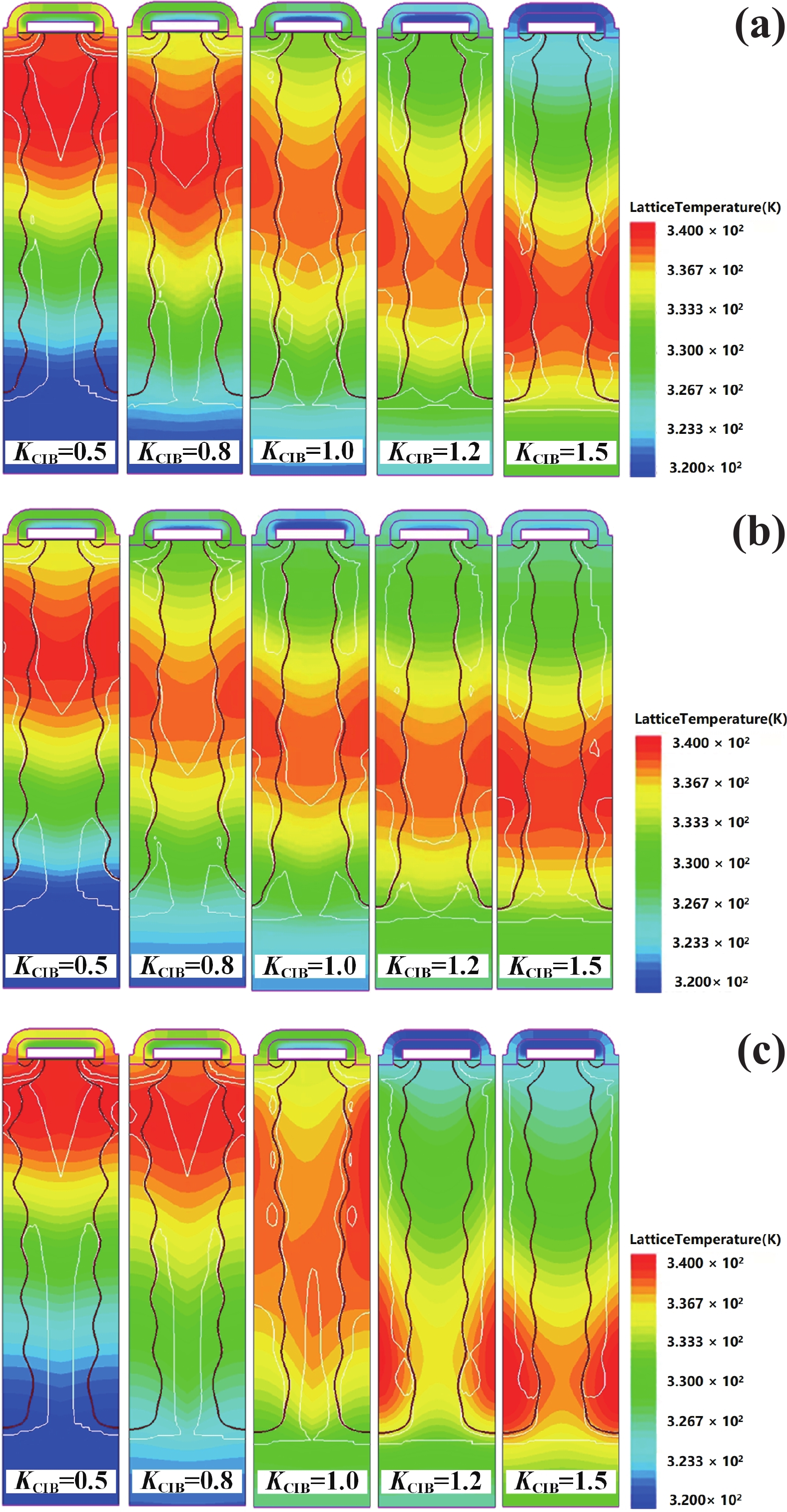
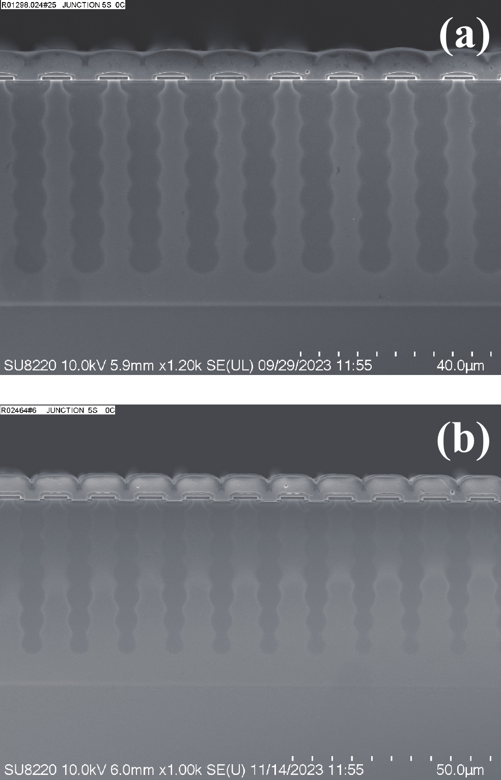
Fig. 1.
(Color online) (a) Half-cell structure and (b) multi-epi process of the VVD-SJ.
ARTICLES
Min Ren1, 3, , Meng Pi1, Rongyao Ma2, Xin Zhang2, Ziyi Zhou1, Qingying Lei1, Lvqiang Li1, Zehong Li1 and Bo Zhang1
Corresponding author: Min Ren, renmin@uestc.edu.cn
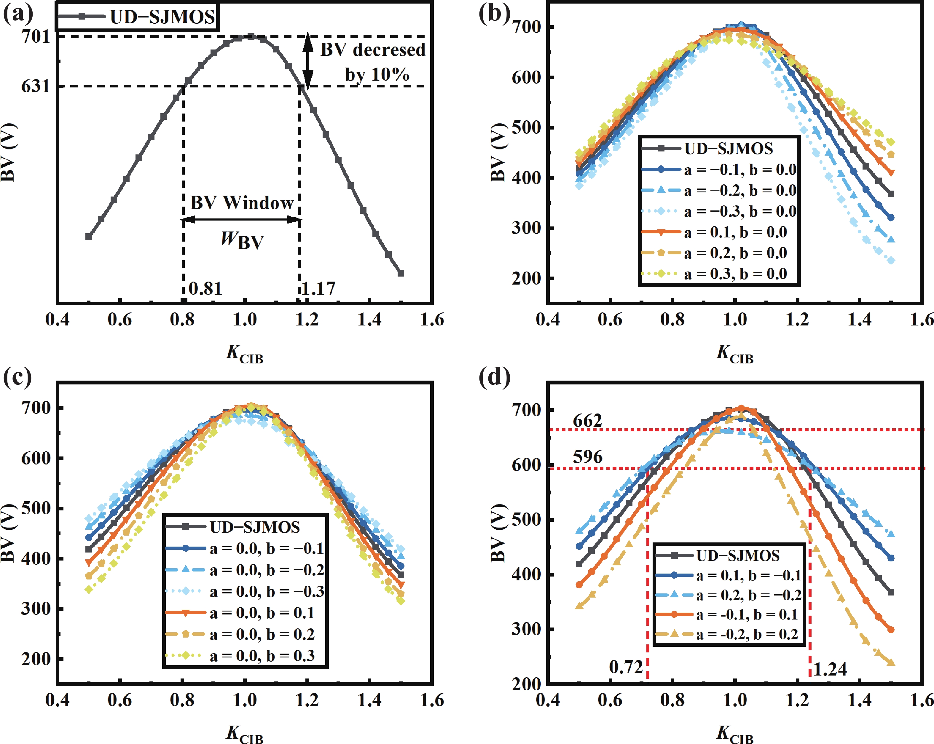
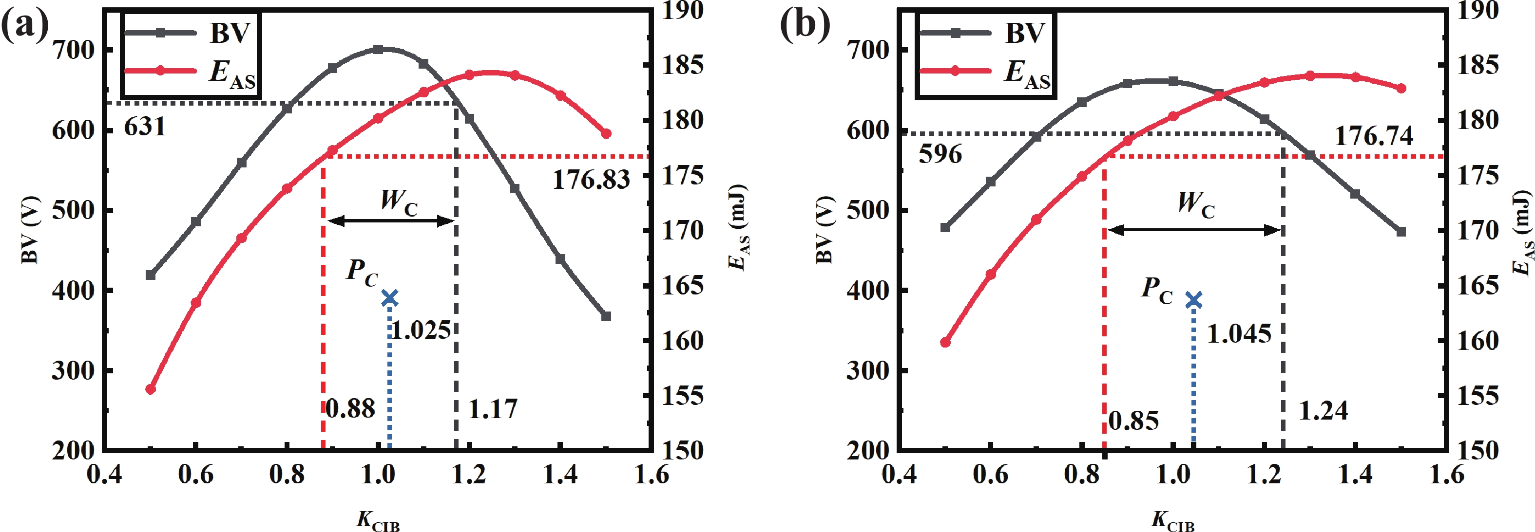
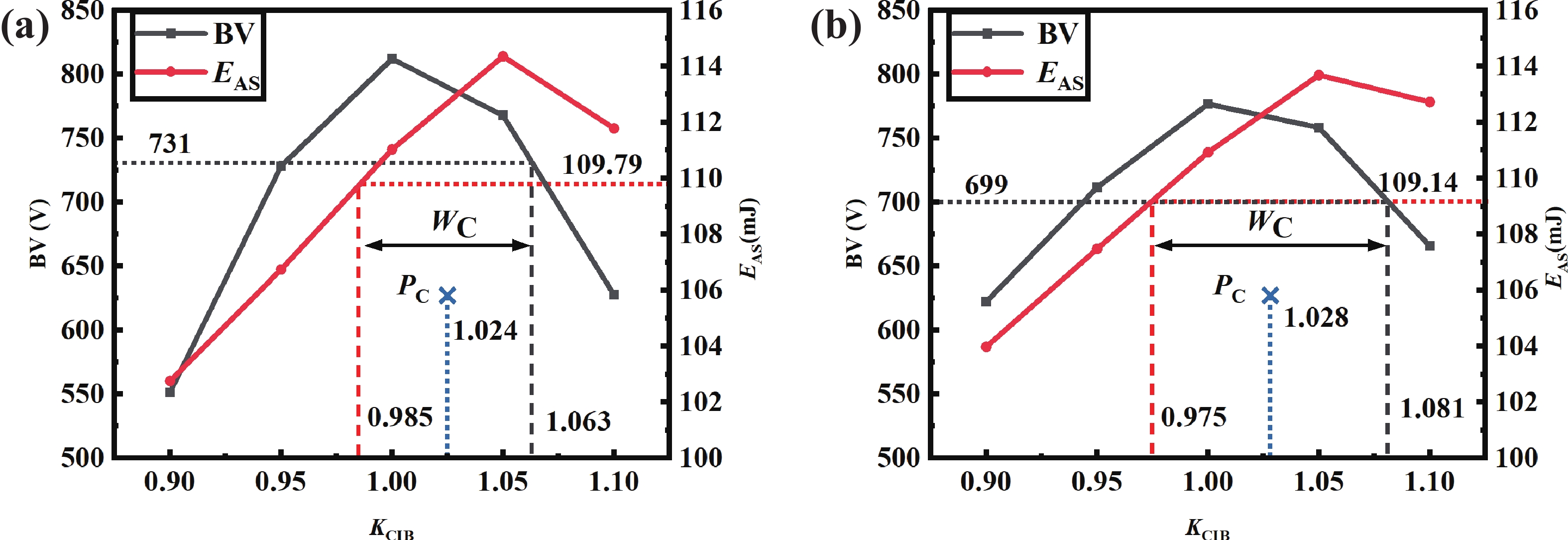
Abstract: As a type of charge-balanced power device, the performance of super-junction MOSFETs (SJ-MOS) is significantly influenced by fluctuations in the fabrication process. To overcome the relatively narrow process window of conventional SJ-MOS, an optimized structure "vertical variable doping super-junction MOSFET (VVD-SJ)" is proposed. Based on the analysis using the charge superposition principle, it is observed that the VVD-SJ, in which the impurity concentration of the P-pillar gradually decreases while that of the N-pillar increases from top to bottom, improves the electric field distribution and mitigates charge imbalance (CIB). Experimental results demonstrate that the optimized 600 V VVD-SJ achieves a 35.90% expansion of the process window.
Keywords: super-junction, charge imbalance, process window, breakdown voltage (BV), unclamped inductive switching (UIS)
| [1] |
Li F C, Guo X R. Development trends and key technologies of 6G green networks. ZTE technology journal, 2023, 29(6), 54 (in Chinese) doi: 10.12142/ZTETJ.202306009
|
| [2] |
Disney D, Shen Z J. Review of silicon power semiconductor technologies for power supply on chip and power supply in package applications. IEEE Trans Power Electron, 2013, 28(9), 4168 doi: 10.1109/TPEL.2013.2242095
|
| [3] |
Liang J R, Li X, Yang H L. Kinetic energy harvesting toward battery-free IoT: Fundamentals, co-design necessity and prospects. ZTE Commun, 2021, 19(1), 48 doi: 10.12142/ZTECOM.202101007
|
| [4] |
Ghandi R, Hitchcock C, Kennerly S, et al. Scalable ultrahigh voltage SiC superjunction device technologies for power electronics applications. IEEE International Electron Devices Meeting (IEDM), 2022, 9.1.1 doi: 10.1109/IEDM45625.2022.10019368.
|
| [5] |
Chen X B, Mawby P A, Board K, et al. Theory of a novel voltage-sustaining layer for power devices. Microelectron J, 1998, 29(12), 1005 doi: 10.1016/S0026-2692(98)00065-2
|
| [6] |
Udrea F, Deboy G, Fujihira T. Superjunction power devices, history, development, and future prospects. IEEE Trans Electron Devices, 2017, 64(3), 713 doi: 10.1109/TED.2017.2658344
|
| [7] |
Zhang W T, Zhang B, Li Z H, et al. Theory of superjunction with NFD and FD modes based on normalized breakdown voltage. IEEE Trans Electron Devices, 2015, 62(12), 4114 doi: 10.1109/TED.2015.2491360
|
| [8] |
Wang C, Li X, Li L, et al. Performance limit and design guideline of 4H-SiC superjunction devices considering anisotropy of impact ionization. IEEE Electron Device Lett, 2022, 43(12), 2025 doi: 10.1109/LED.2022.3212465
|
| [9] |
Napoli E, Wang H, Udrea F. The effect of charge imbalance on superjunction power devices: An exact analytical solution. IEEE Electron Device Lett, 2008, 29(3), 249 doi: 10.1109/LED.2007.915375
|
| [10] |
Wang H, Napoli E, Udrea F. Breakdown voltage for superjunction power devices with charge imbalance: An analytical model valid for both punch through and non punch through devices. IEEE Trans Electron Devices, 2009, 56(12), 3175 doi: 10.1109/TED.2009.2032595
|
| [11] |
Saito W. Theoretical limits of superjunction considering with charge imbalance margin. 2015 IEEE 27th International Symposium on Power Semiconductor Devices & IC’s (ISPSD), 2015, 125 doi: 10.1109/ISPSD.2015.7123405
|
| [12] |
Ren M, Li L Q, Lan Y Y, et al. The superjunction device with optimized process window of breakdown voltage. 2020 IEEE 15th International Conference on Solid-State & Integrated Circuit Technology (ICSICT), 2020, 1 doi: 10.1109/ICSICT49897.2020.9278209
|
| [13] |
Li X, Li L F, Xie K Z, et al. Charge imbalance tolerance of 4H-SiC superjunction devices featuring breakdown path variation. IEEE Electron Device Lett, 2023, 44(7), 1044 doi: 10.1109/LED.2023.3281328
|
| [14] |
Tamaki T, Inoue A, Furuhashi M, et al. Dynamic charge imbalance in superjunction IGBTs: Design, simulation, and experimental validation. 2024 36th International Symposium on Power Semiconductor Devices and ICs (ISPSD), 2024, 558 doi: 10.1109/ISPSD59661.2024.10579470
|
| [15] |
Alatise O, Kennedy I, Petkos G, et al. The impact of repetitive unclamped inductive switching on the electrical parameters of low-voltage trench power nMOSFETs. IEEE Trans Electron Devices, 2010, 57, 1651 doi: 10.1109/TED.2010.2049062
|
| [16] |
Roig J, Moens P, McDonald J, et al. Energy limits for unclamped inductive switching in high-voltage planar and superjunction power MOSFETs. 2011 IEEE 23rd International Symposium on Power Semiconductor Devices and ICs, 2011, 312 doi: 10.1109/ISPSD.2011.5890853
|
| [17] |
Honda M, Yamaji M, Arai D, et al. Influence of external gate resistance on UIS capability in superjunction MOSFET. 2019 31st International Symposium on Power Semiconductor Devices and ICs (ISPSD), 2019, 335 doi: 10.1109/ISPSD.2019.8757613
|
| [18] |
Liu S Y, Tong X, Wei J X, et al. Single-pulse avalanche failure investigations of Si-SJ-mosfet and SiC-mosfet by step-control infrared thermography method. IEEE Trans Power Electron, 2020, 35(5), 5180 doi: 10.1109/TPEL.2019.2946792
|
| [19] |
Tong X, Liu S Y, Sun W F, et al. New failure mechanism induced by current limit for superjunction MOSFET under single-pulse UIS stress. IEEE Trans Electron Devices, 2021, 68(7), 3483 doi: 10.1109/TED.2021.3078718
|
| [20] |
Gao Z J, Guo Q, Ren N, et al. Experimental investigation on failure mechanism of SiC power MOSFETs under single pulse avalanche stress. 2020 IEEE Workshop on Wide Bandgap Power Devices and Applications in Asia (WiPDA Asia), 2020, 1 doi: 10.1109/WiPDAAsia49671.2020.9360260
|


Article views: 2161 Times PDF downloads: 319 Times Cited by: 0 Times
Received: 26 July 2024 Revised: 27 November 2024 Online: Accepted Manuscript: 13 January 2025Uncorrected proof: 18 February 2025Published: 05 June 2025
| Citation: |
Min Ren, Meng Pi, Rongyao Ma, Xin Zhang, Ziyi Zhou, Qingying Lei, Lvqiang Li, Zehong Li, Bo Zhang. Theoretical and experimental study on the vertical-variable-doping superjunction MOSFET with optimized process window[J]. Journal of Semiconductors, 2025, 46(6): 062302. doi: 10.1088/1674-4926/24070029
****
M Ren, M Pi, R Y Ma, X Zhang, Z Y Zhou, Q Y Lei, L Q Li, Z H Li, and B Zhang, Theoretical and experimental study on the vertical-variable-doping superjunction MOSFET with optimized process window[J]. J. Semicond., 2025, 46(6), 062302 doi: 10.1088/1674-4926/24070029

|
 Min Ren received the Ph.D. degree from Tsinghua University, Beijing, China, in 2009. She is currently a Professor with the University of Electronic Science and Technology of China, Chengdu, China. Her research interests are in power semiconductor devices and integrated circuits
 Meng Pi received the B.S. degree in microelectronics from University of Electronic Science and Technology of China, Chengdu, China, in 2022. Currently, he is pursuing his master degree at UESTC under the supervision of Professor Min Ren. His research interests focus on semiconductor physical devices and integrated circuits
| [1] |
Li F C, Guo X R. Development trends and key technologies of 6G green networks. ZTE technology journal, 2023, 29(6), 54 (in Chinese) doi: 10.12142/ZTETJ.202306009
|
| [2] |
Disney D, Shen Z J. Review of silicon power semiconductor technologies for power supply on chip and power supply in package applications. IEEE Trans Power Electron, 2013, 28(9), 4168 doi: 10.1109/TPEL.2013.2242095
|
| [3] |
Liang J R, Li X, Yang H L. Kinetic energy harvesting toward battery-free IoT: Fundamentals, co-design necessity and prospects. ZTE Commun, 2021, 19(1), 48 doi: 10.12142/ZTECOM.202101007
|
| [4] |
Ghandi R, Hitchcock C, Kennerly S, et al. Scalable ultrahigh voltage SiC superjunction device technologies for power electronics applications. IEEE International Electron Devices Meeting (IEDM), 2022, 9.1.1 doi: 10.1109/IEDM45625.2022.10019368.
|
| [5] |
Chen X B, Mawby P A, Board K, et al. Theory of a novel voltage-sustaining layer for power devices. Microelectron J, 1998, 29(12), 1005 doi: 10.1016/S0026-2692(98)00065-2
|
| [6] |
Udrea F, Deboy G, Fujihira T. Superjunction power devices, history, development, and future prospects. IEEE Trans Electron Devices, 2017, 64(3), 713 doi: 10.1109/TED.2017.2658344
|
| [7] |
Zhang W T, Zhang B, Li Z H, et al. Theory of superjunction with NFD and FD modes based on normalized breakdown voltage. IEEE Trans Electron Devices, 2015, 62(12), 4114 doi: 10.1109/TED.2015.2491360
|
| [8] |
Wang C, Li X, Li L, et al. Performance limit and design guideline of 4H-SiC superjunction devices considering anisotropy of impact ionization. IEEE Electron Device Lett, 2022, 43(12), 2025 doi: 10.1109/LED.2022.3212465
|
| [9] |
Napoli E, Wang H, Udrea F. The effect of charge imbalance on superjunction power devices: An exact analytical solution. IEEE Electron Device Lett, 2008, 29(3), 249 doi: 10.1109/LED.2007.915375
|
| [10] |
Wang H, Napoli E, Udrea F. Breakdown voltage for superjunction power devices with charge imbalance: An analytical model valid for both punch through and non punch through devices. IEEE Trans Electron Devices, 2009, 56(12), 3175 doi: 10.1109/TED.2009.2032595
|
| [11] |
Saito W. Theoretical limits of superjunction considering with charge imbalance margin. 2015 IEEE 27th International Symposium on Power Semiconductor Devices & IC’s (ISPSD), 2015, 125 doi: 10.1109/ISPSD.2015.7123405
|
| [12] |
Ren M, Li L Q, Lan Y Y, et al. The superjunction device with optimized process window of breakdown voltage. 2020 IEEE 15th International Conference on Solid-State & Integrated Circuit Technology (ICSICT), 2020, 1 doi: 10.1109/ICSICT49897.2020.9278209
|
| [13] |
Li X, Li L F, Xie K Z, et al. Charge imbalance tolerance of 4H-SiC superjunction devices featuring breakdown path variation. IEEE Electron Device Lett, 2023, 44(7), 1044 doi: 10.1109/LED.2023.3281328
|
| [14] |
Tamaki T, Inoue A, Furuhashi M, et al. Dynamic charge imbalance in superjunction IGBTs: Design, simulation, and experimental validation. 2024 36th International Symposium on Power Semiconductor Devices and ICs (ISPSD), 2024, 558 doi: 10.1109/ISPSD59661.2024.10579470
|
| [15] |
Alatise O, Kennedy I, Petkos G, et al. The impact of repetitive unclamped inductive switching on the electrical parameters of low-voltage trench power nMOSFETs. IEEE Trans Electron Devices, 2010, 57, 1651 doi: 10.1109/TED.2010.2049062
|
| [16] |
Roig J, Moens P, McDonald J, et al. Energy limits for unclamped inductive switching in high-voltage planar and superjunction power MOSFETs. 2011 IEEE 23rd International Symposium on Power Semiconductor Devices and ICs, 2011, 312 doi: 10.1109/ISPSD.2011.5890853
|
| [17] |
Honda M, Yamaji M, Arai D, et al. Influence of external gate resistance on UIS capability in superjunction MOSFET. 2019 31st International Symposium on Power Semiconductor Devices and ICs (ISPSD), 2019, 335 doi: 10.1109/ISPSD.2019.8757613
|
| [18] |
Liu S Y, Tong X, Wei J X, et al. Single-pulse avalanche failure investigations of Si-SJ-mosfet and SiC-mosfet by step-control infrared thermography method. IEEE Trans Power Electron, 2020, 35(5), 5180 doi: 10.1109/TPEL.2019.2946792
|
| [19] |
Tong X, Liu S Y, Sun W F, et al. New failure mechanism induced by current limit for superjunction MOSFET under single-pulse UIS stress. IEEE Trans Electron Devices, 2021, 68(7), 3483 doi: 10.1109/TED.2021.3078718
|
| [20] |
Gao Z J, Guo Q, Ren N, et al. Experimental investigation on failure mechanism of SiC power MOSFETs under single pulse avalanche stress. 2020 IEEE Workshop on Wide Bandgap Power Devices and Applications in Asia (WiPDA Asia), 2020, 1 doi: 10.1109/WiPDAAsia49671.2020.9360260
|

 WeChat ID
Journal of Semiconductors © 2017 All Rights Reserved 京ICP备05085259号-2

 DownLoad: