Fig. 1.
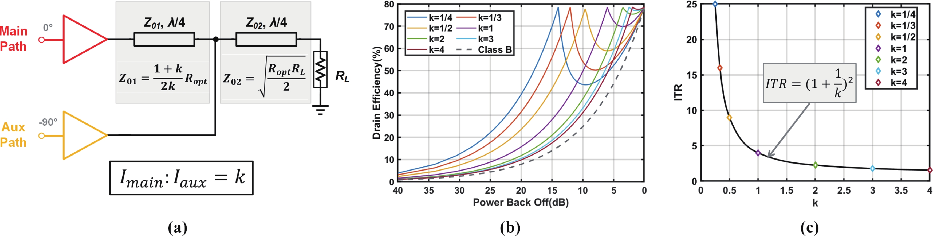
(Color online) Two-way PDPA’s. (a) Simplified model; (b) drain efficiency performance; (c) λ/4 T-line based IIN’s ITR.
SPECIAL TOPIC ARTICLES
Xinyu Jiang, Wei Deng, Junlong Gong, Haikun Jia and Baoyong Chi
Corresponding author: Wei Deng, wdeng@tsinghua.edu.cn
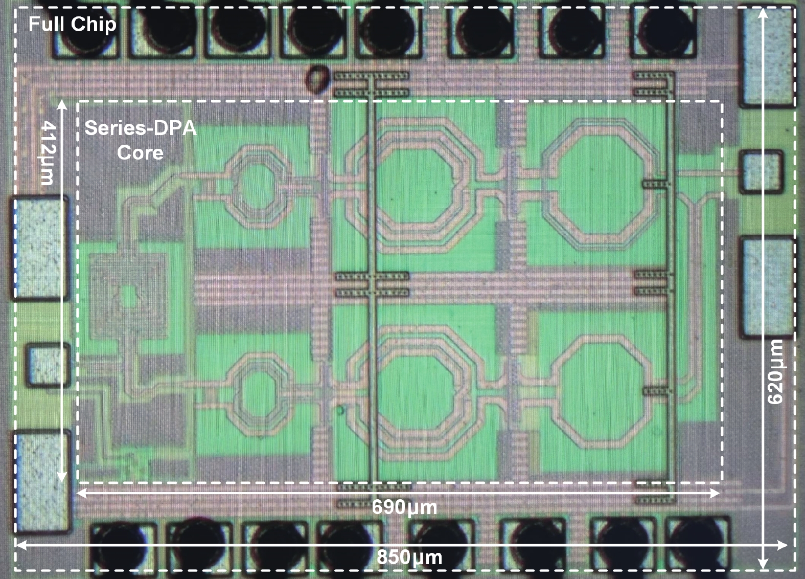
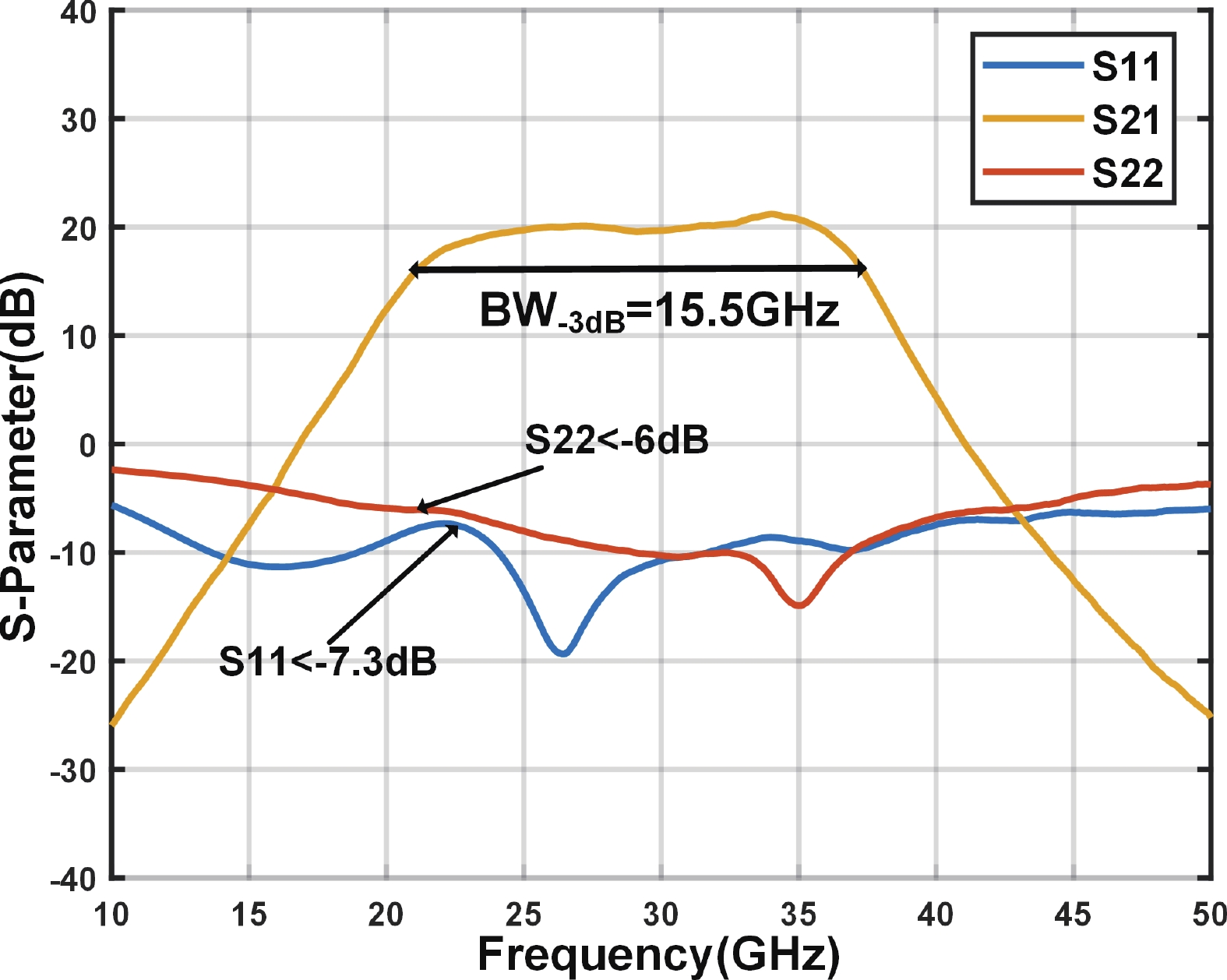
Abstract: A two-way K/Ka-band series-Doherty PA (SDPA) with a distributed impedance inverting network (IIN) for millimeter wave applications is presented in this article. The proposed distributed IIN contributes to achieve wideband linear and power back-off (PBO) efficiency enhancement. Implemented in 65 nm bulk CMOS technology, this work realizes a measured 3 dB bandwidth of 15.5 GHz with 21.2 dB peak small-signal gain at 34.2 GHz. Under 1-V power supply, it achieves OP1dB over 13.4 dBm and Psat over 16 dBm between 21 to 30 GHz. The measured maximum Psat, OP1dB, peak/OP1dB/6dBPBO PAE results are 17.5, 14.7 dBm, and 28.2%/23.2%/13.2%. Without digital pre-distortion (DPD) and equalization, EVMs are lower than −25.2 dB for 200 MHz 64-QAM signals. Besides, this work achieves −33.35, −23.52, and −20 dB EVMs for 100 MHz 256-QAM, 600 MHz 64-QAM and 2 GHz 16-QAM signals at 27 GHz without DPD and equalization.
Keywords: Doherty PA, load modulation, broadband, transformer, linear enhancement, efficiency enhancement
| [1] |
Pashaeifar M, de Vreede L C N, Alavi M S. A millimeter-wave CMOS series-Doherty power amplifier with post-silicon inter-stage passive validation. IEEE J Solid State Circuits, 2022, 57(10), 2999 doi: 10.1109/JSSC.2022.3175685
|
| [2] |
Wang Y, Xu H T. Millimeter-wave PA design techniques in ISSCC 2024. J Semicond, 2024, 45(4), 040205 doi: 10.1088/1674-4926/45/4/040205
|
| [3] |
Li S S, Huang M Y, Jung D, et al. A MM-wave current-mode inverse outphasing transmitter front-end: A circuit duality of conventional voltage-mode outphasing. IEEE J Solid State Circuits, 2021, 56(6), 1732 doi: 10.1109/JSSC.2020.3038882
|
| [4] |
Rabet B, Asbeck P M. A 28 GHz single-input linear chireix (SILC) power amplifier in 130 nm SiGe technology. IEEE J Solid State Circuits, 2020, 55(6), 1482 doi: 10.1109/JSSC.2020.2967542
|
| [5] |
Anabtawi N, Ferzli R, Harmanani H M. A single switcher combined series parallel hybrid envelope tracking amplifier for wideband RF power amplifier applications. 2016 IEEE International Symposium on Circuits and Systems (ISCAS), 2016, 2366 doi: 10.1109/ISCAS.2016.7539060
|
| [6] |
Chowdhury D, Mundlapudi S R, Afsahi A. A fully integrated reconfigurable wideband envelope-tracking SoC for high-bandwidth WLAN applications in a 28nm CMOS technology. 2017 IEEE International Solid-State Circuits Conference (ISSCC), 2017, 34 doi: 10.1109/ISSCC.2017.7870247
|
| [7] |
Qunaj V, Reynaert P. A ka-band Doherty-like LMBA for high-speed wireless communication in 28-nm CMOS. IEEE J Solid State Circuits, 2021, 56(12), 3694 doi: 10.1109/JSSC.2021.3110168
|
| [8] |
Huang X R, Jia H K, Deng W, et al. A compact E-band load-modulation balanced power amplifier in 65-nm CMOS. IEEE J Solid State Circuits, 2024, 59(10), 3172 doi: 10.1109/JSSC.2024.3404610
|
| [9] |
Rostomyan N, Özen M, Asbeck P. 28 GHz Doherty power amplifier in CMOS SOI with 28% back-off PAE. IEEE Microw Wirel Compon Lett, 2018, 28(5), 446 doi: 10.1109/LMWC.2018.2813882
|
| [10] |
Park H C, Kim S, Lee J, et al. Single transformer-based compact Doherty power amplifiers for 5G RF phased-array ICs. IEEE J Solid State Circuits, 2022, 57(5), 1267 doi: 10.1109/JSSC.2022.3148044
|
| [11] |
Cripps S C. RF power amplifiers for wireless communications, 2nd ed. Norwood, MA: Artech House, 2006
|
| [12] |
Yi Y R, Zhao D X, Zhang J J, et al. A 24–30 GHz 8-element dual-polarized 5g Fr2 phased-array transceiveric with 20.8-dBm tx OP1dB and 4.1-dB rx NFin 65-nm cmos. J Semicond, 2024, 45(1), 012201 doi: 10.1088/1674-4926/45/1/012201
|
| [13] |
Jia H K, Prawoto C C, Chi B Y, et al. A full ka-band power amplifier with 32.9% PAE and 15.3-dBm power in 65-nm CMOS. IEEE Trans Circuits Syst I Regul Pap, 2018, 65(9), 2657 doi: 10.1109/TCSI.2018.2799983
|
| [14] |
Wang R T, Li C G, Qiu K Q, et al. A ka-band broadband power amplifier with transformer-based lossy magnetically coupled resonator network: Analysis and design. IEEE Trans Microw Theory Tech, 2024, 72(12), 6857 doi: 10.1109/TMTT.2024.3411485
|
| [15] |
Gong J, Li W, Hu J T, et al. An 8–18 GHz power amplifier with novel gain fluctuation compensation technique in 65 nm CMOS. J Semicond, 2018, 39(12), 125008 doi: 10.1088/1674-4926/39/12/125008
|
| [16] |
Chan W L, Long J R. A 58–65 GHz neutralized CMOS power amplifier with PAE above 10% at 1-V supply. IEEE J Solid State Circuits, 2010, 45(3), 554 doi: 10.1109/JSSC.2009.2039274
|
| [17] |
Hu S, Wang F, Wang H. A 28-/37-/39-GHz linear Doherty power amplifier in silicon for 5G applications. IEEE J Solid State Circuits, 2019, 54(6), 1586 doi: 10.1109/JSSC.2019.2902307
|
| [18] |
Wang F, Wang H. A high-power broadband multi-primary DAT-based Doherty power amplifier for mm-wave 5G applications. IEEE J Solid State Circuits, 2021, 56(6), 1668 doi: 10.1109/JSSC.2021.3070800
|
| [19] |
Zhang X H, Li S S, Huang D Q, et al. A millimeter-wave three-way Doherty power amplifier for 5G NR OFDM. IEEE J Solid State Circuits, 2023, 58(5), 1256 doi: 10.1109/JSSC.2023.3238766
|
| [20] |
Kulkarni S, Zhao D X, Reynaert P. Design of an optimal layout polyphase filter for millimeter-wave quadrature LO generation. IEEE Trans Circuits Syst II Express Briefs, 2013, 60(4), 202 doi: 10.1109/TCSII.2013.2251946
|
| [21] |
Koh K J, Rebeiz G M. 0.13-μm CMOS phase shifters for X-, Ku-, and K-band phased arrays. IEEE J Solid State Circuits, 2007, 42(11), 2535 doi: 10.1109/JSSC.2007.907225
|
| [22] |
Indirayanti P, Reynaert P. A 32 GHz 20 dBm-PSAT transformer-based Doherty power amplifier for multi-Gb/s 5G applications in 28 nm bulk CMOS. 2017 IEEE Radio Frequency Integrated Circuits Symposium (RFIC), 2017, 45 doi: 10.1109/RFIC.2017.7969013
|
| [23] |
Fang X H, Xia J J, Boumaiza S. A 28-GHz beamforming Doherty power amplifier with enhanced AM-PM characteristic. IEEE Trans Microw Theory Tech, 2020, 68(7), 3017 doi: 10.1109/TMTT.2020.2968318
|
| [24] |
Yu C Y, Feng J, Zhao D X. A 28-GHz Doherty power amplifier with a compact transformer-based quadrature hybrid in 65-nm CMOS. IEEE Trans Circuits Syst II Express Briefs, 2021, 68(8), 2790 doi: 10.1109/TCSII.2021.3068473
|
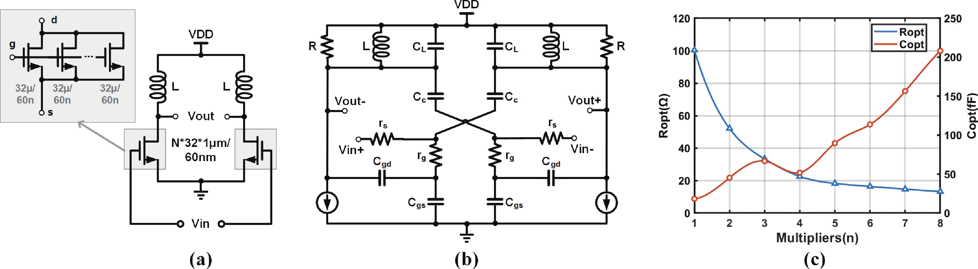
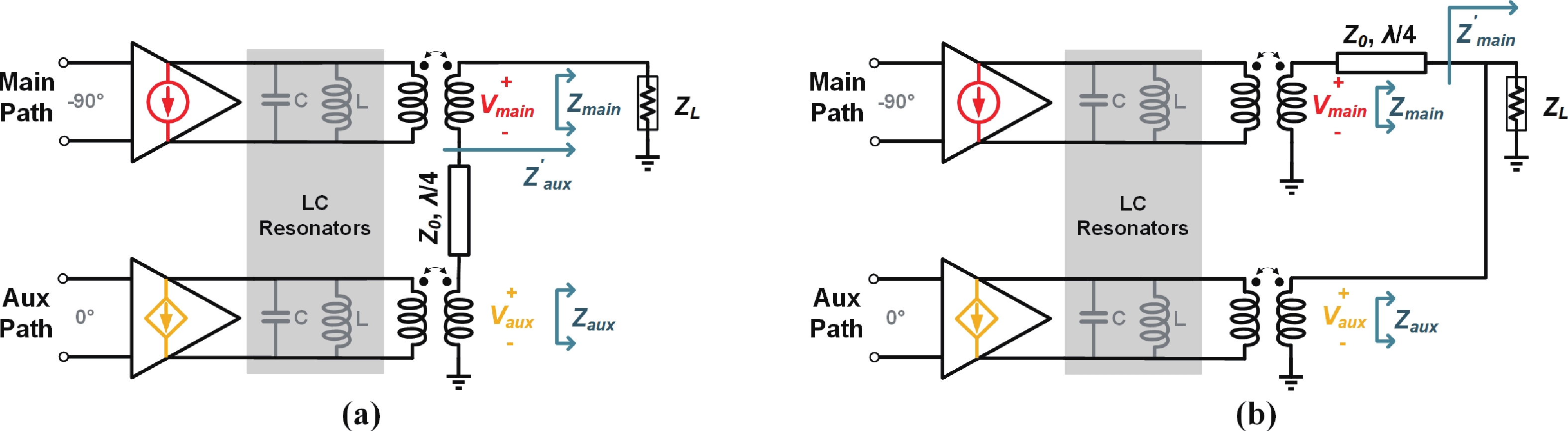
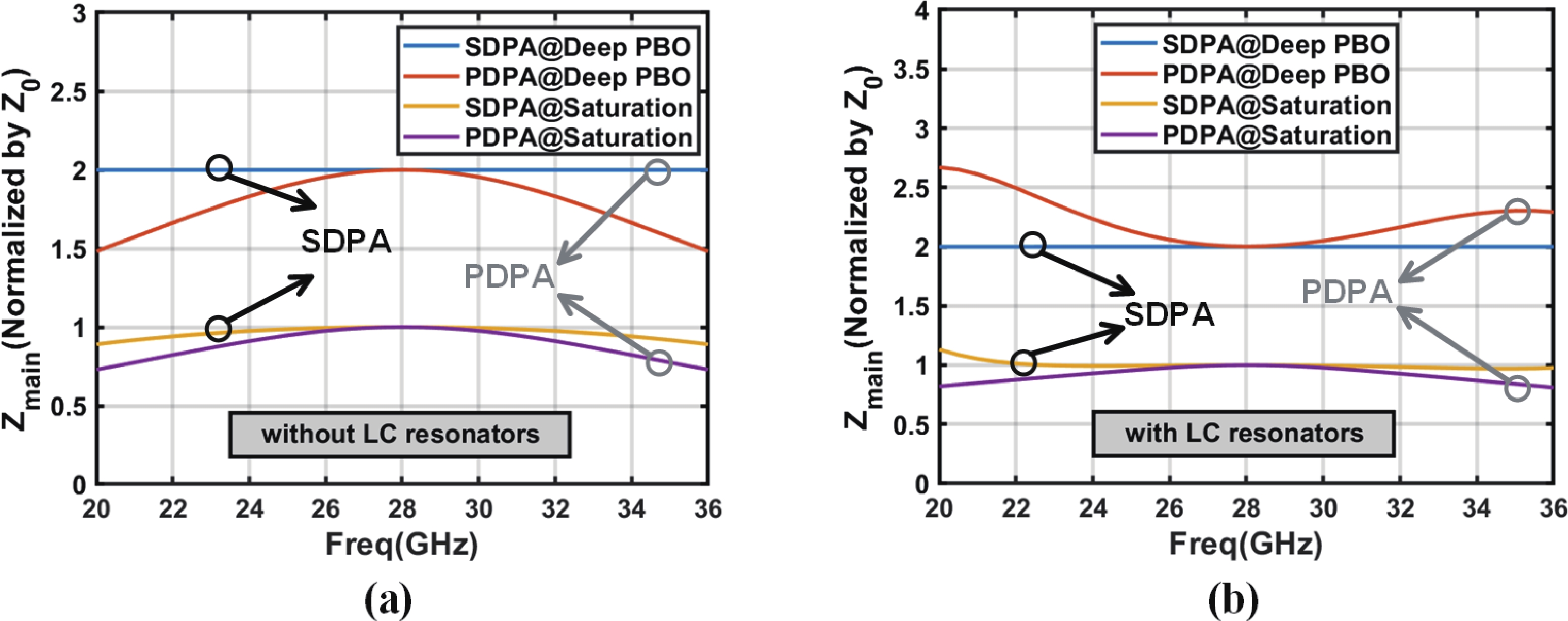
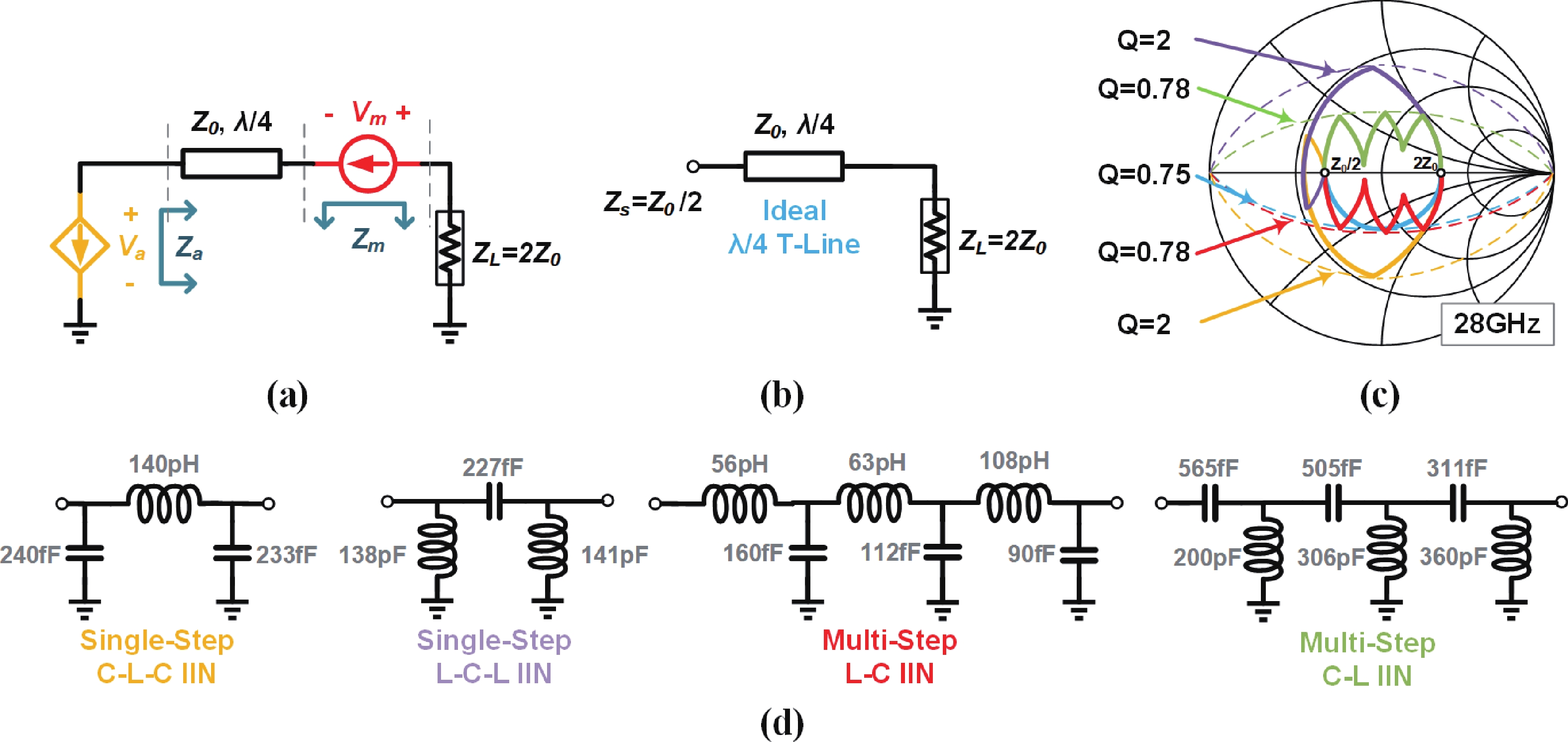
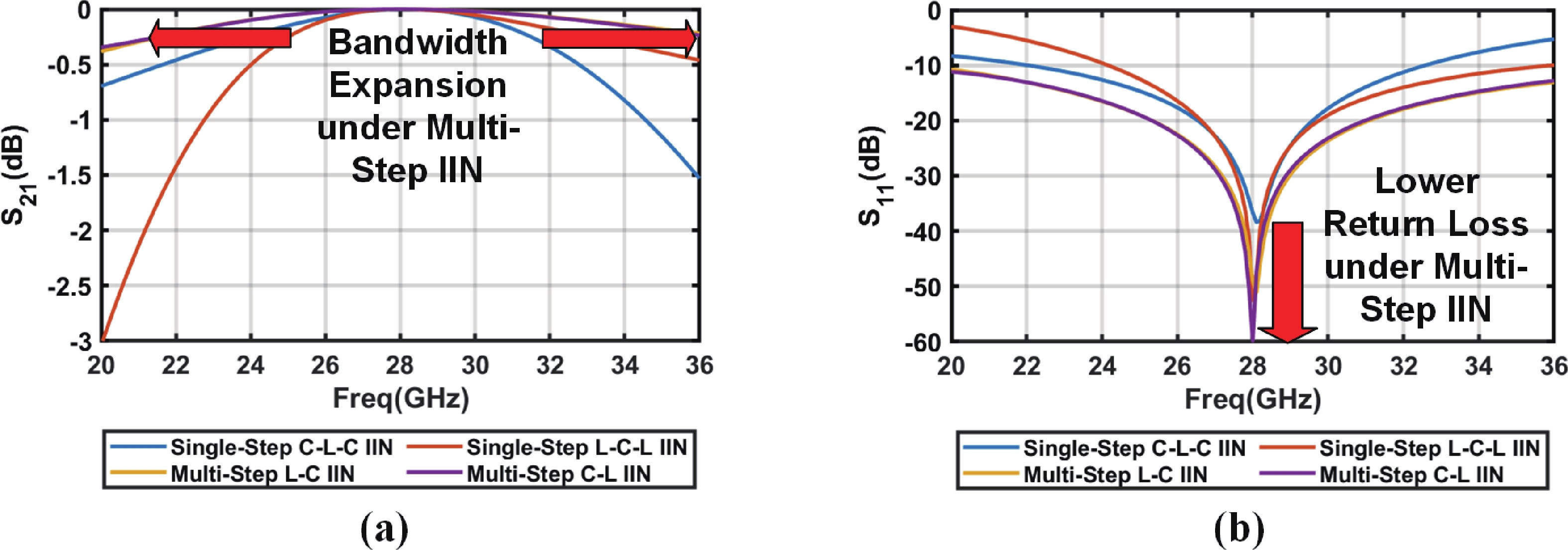
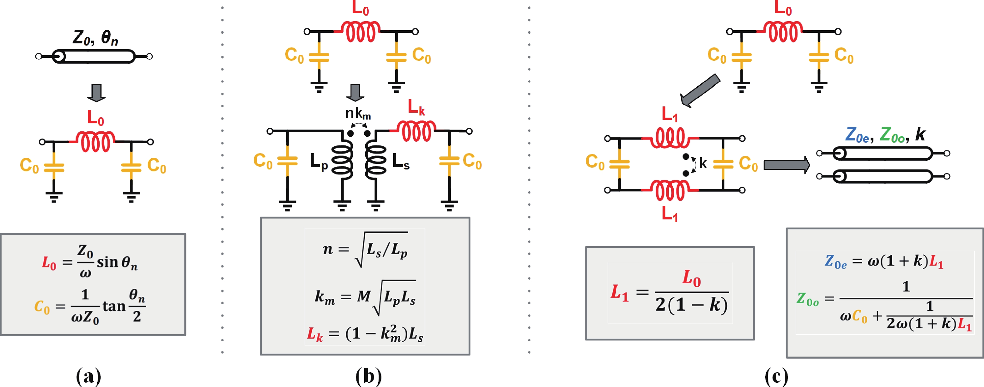
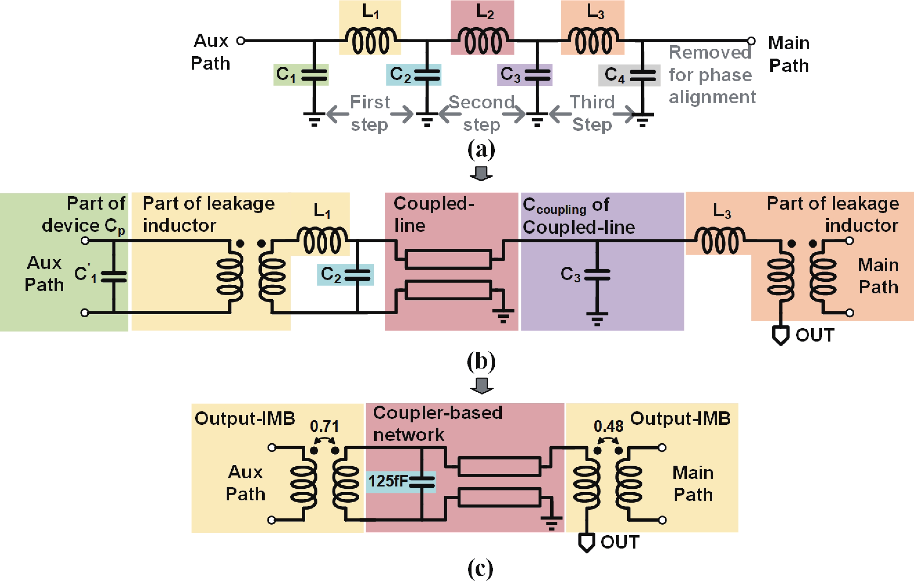
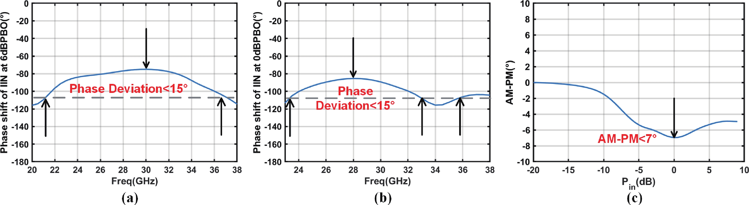
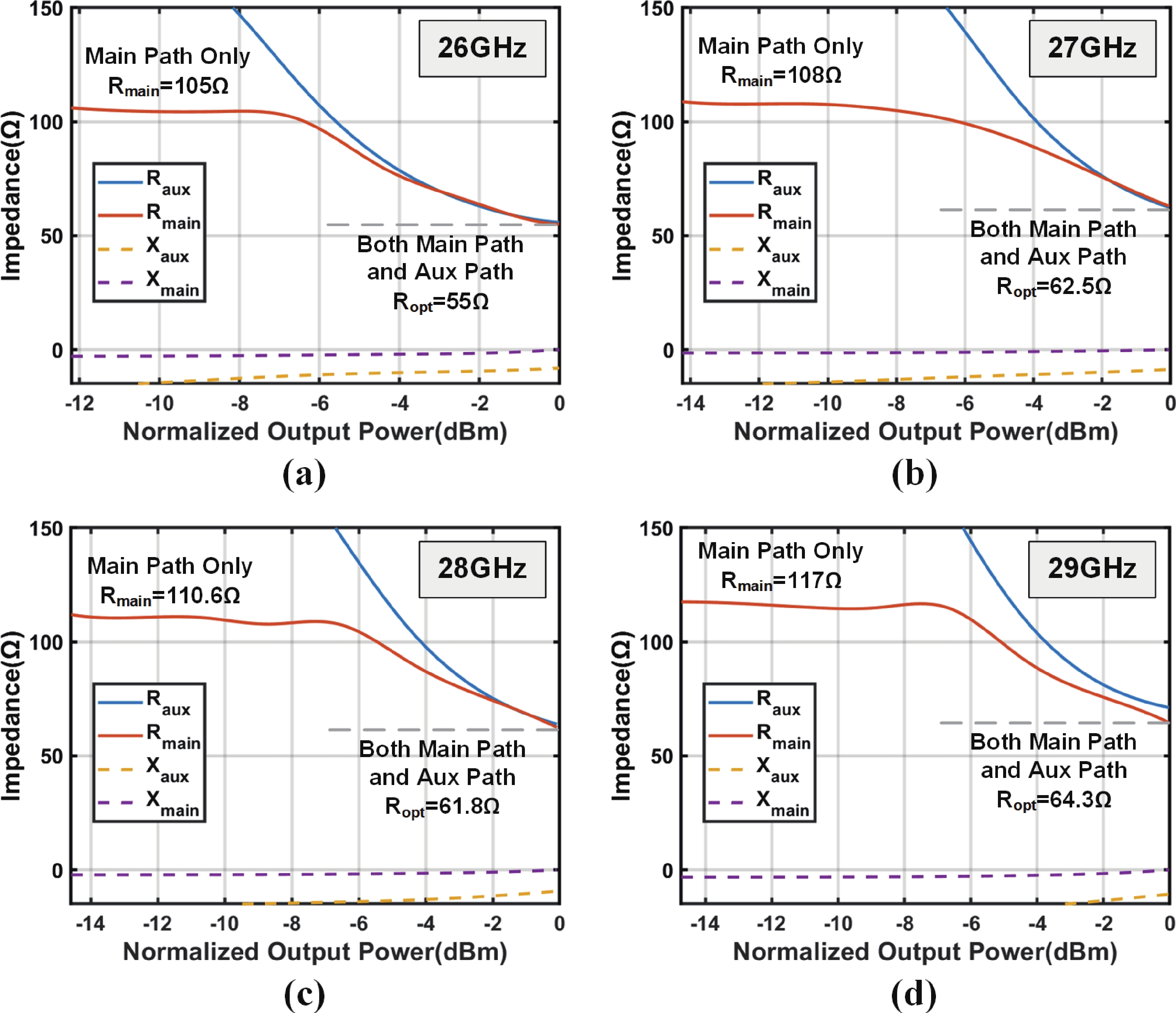
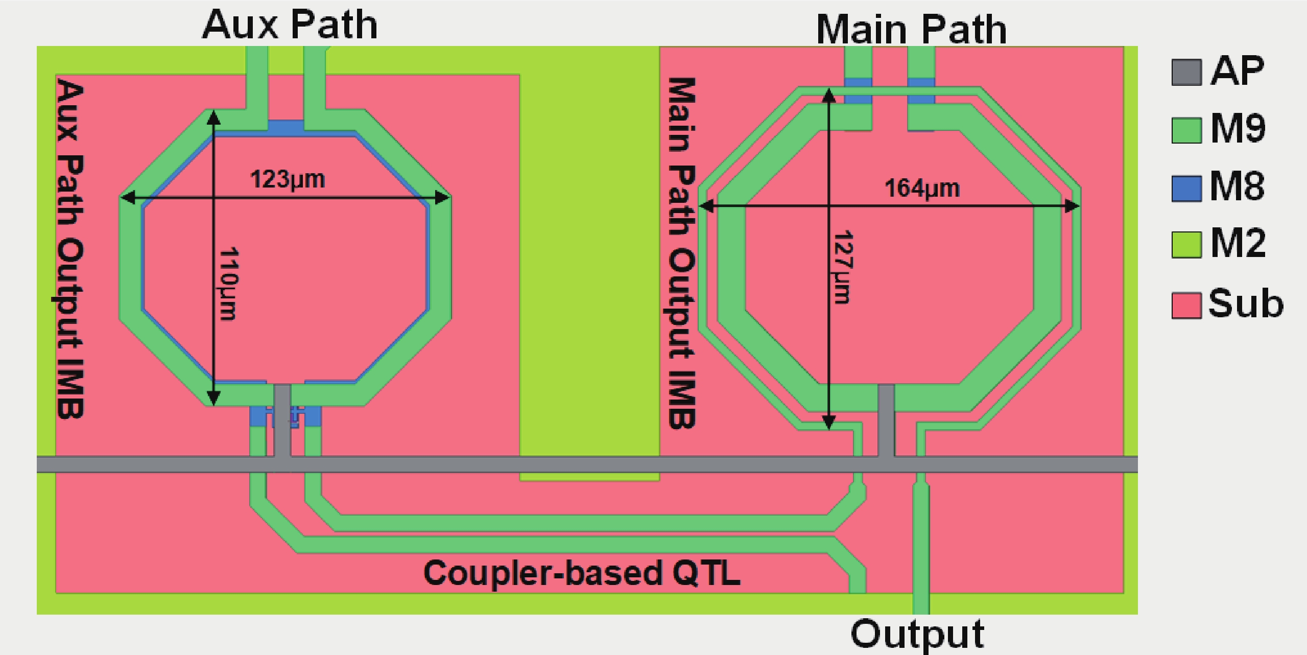
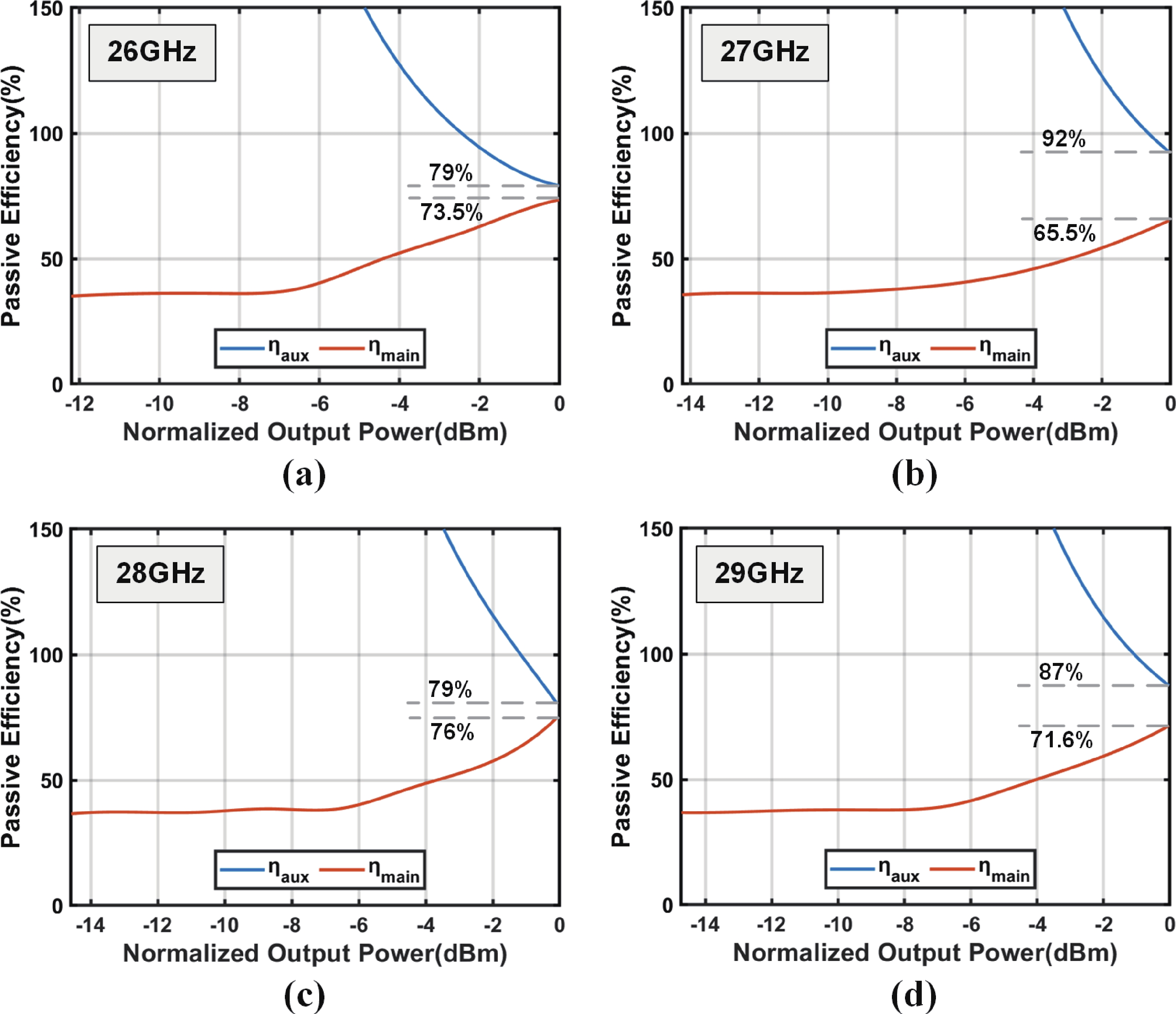
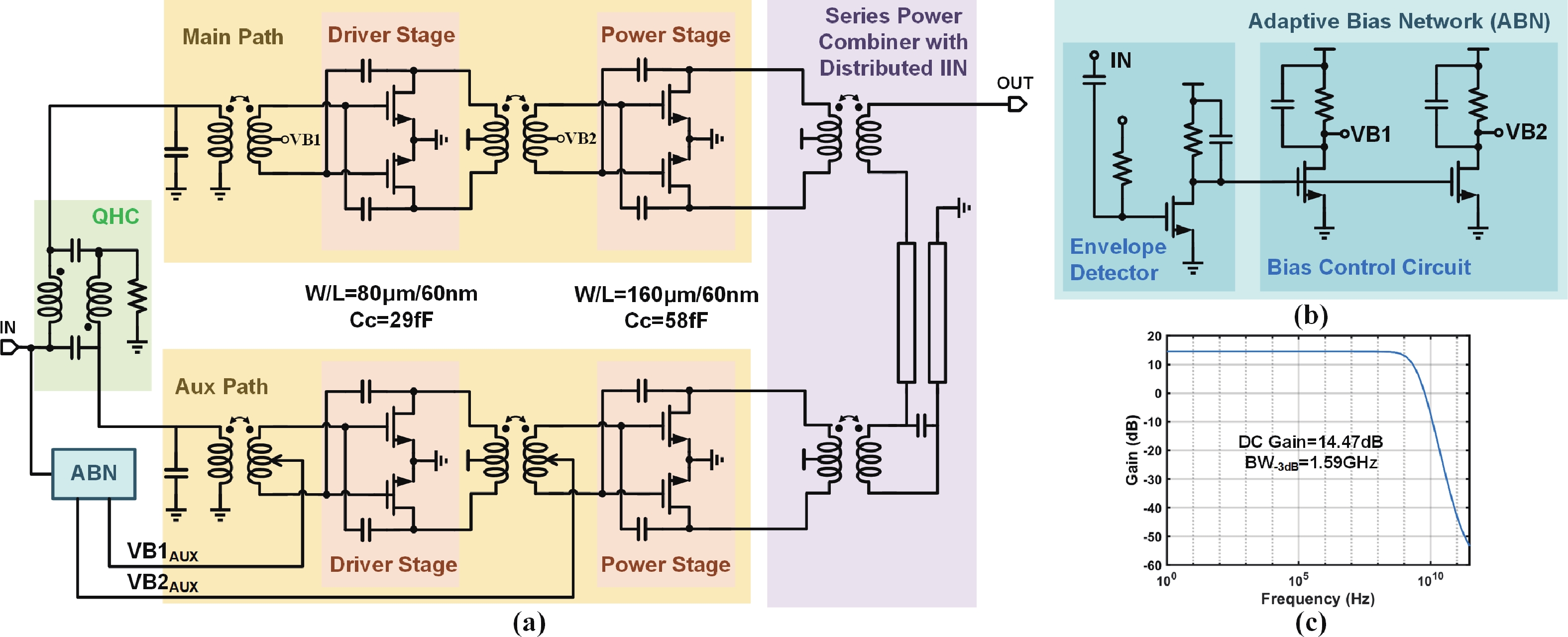
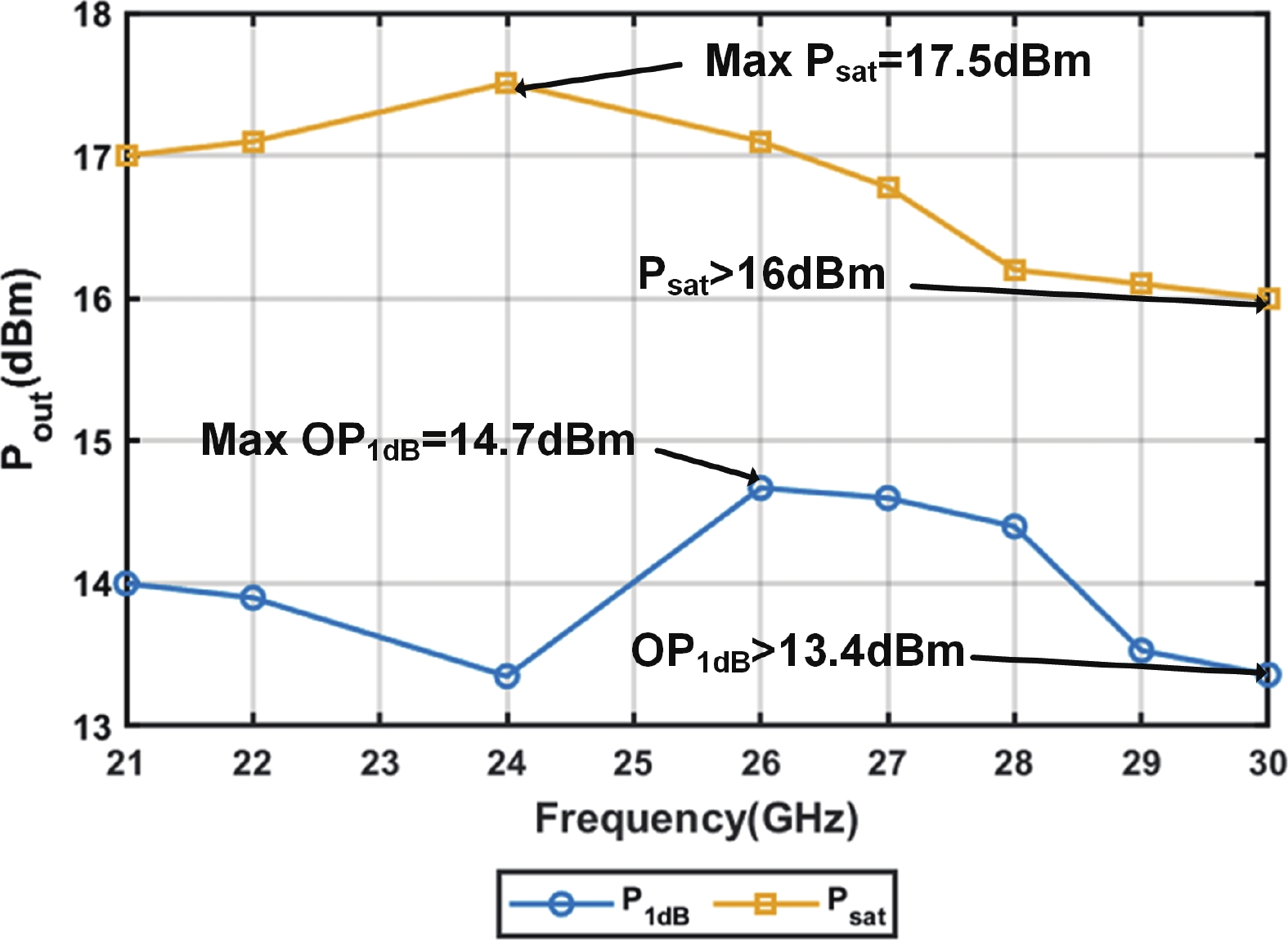
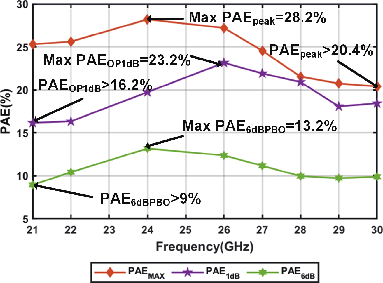
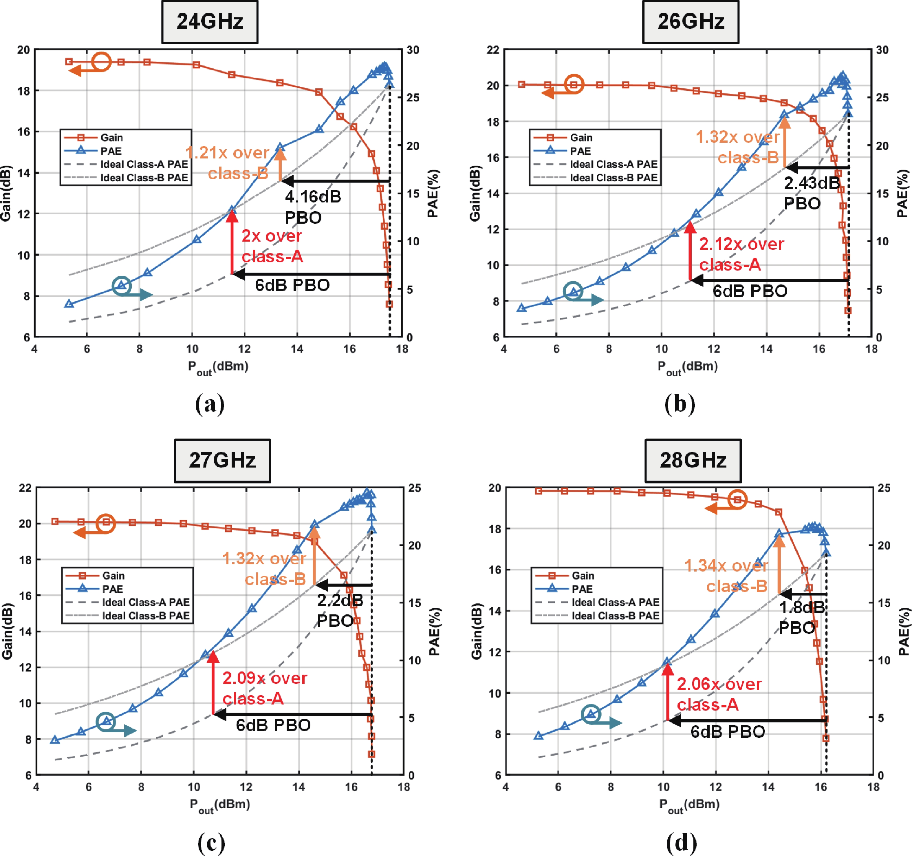
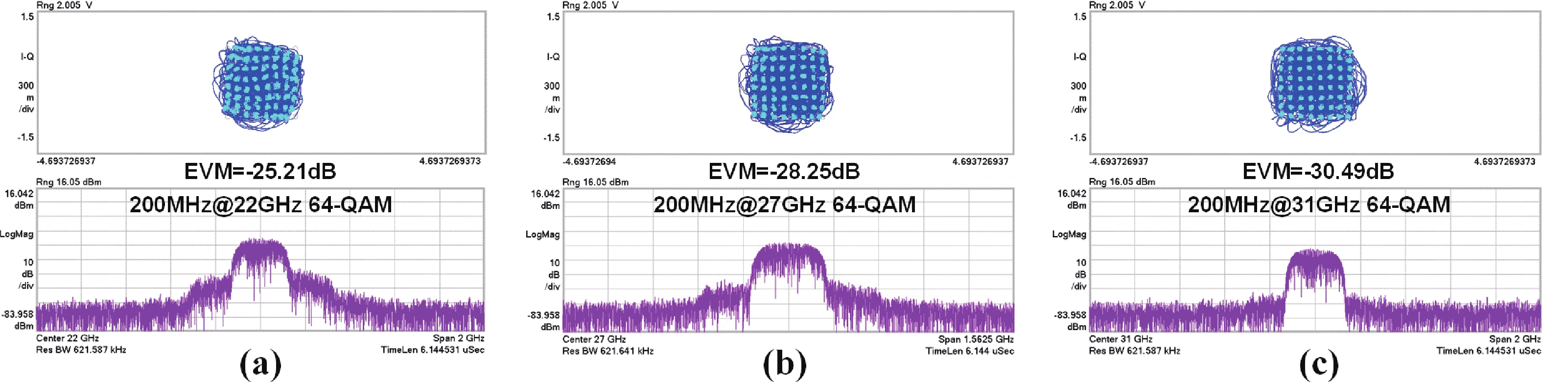
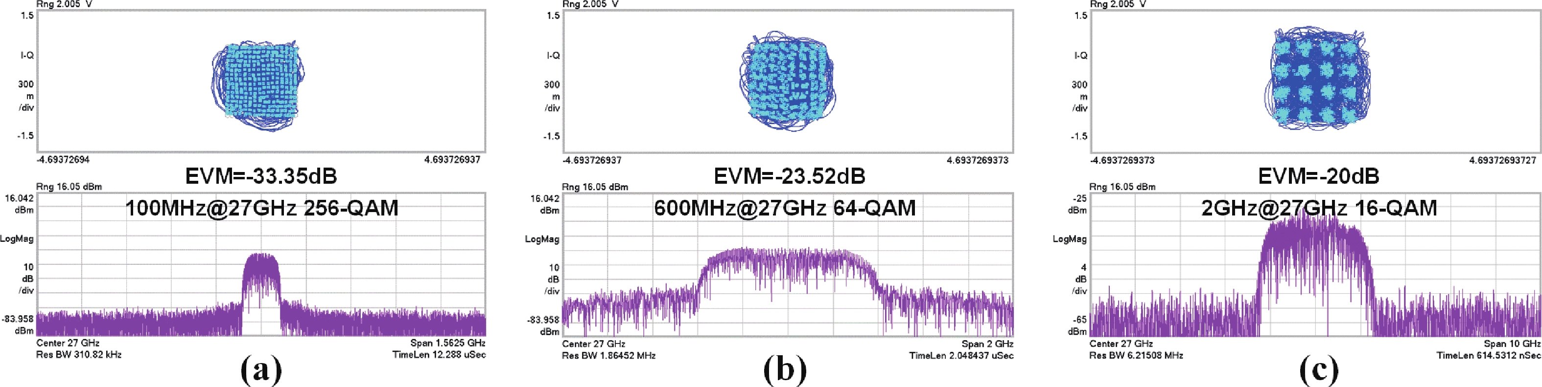
Table 1. Performance comparison.
| Design parameters | RFIC 2017[22] | TMTT 2020[23] | TCAS-II 2021[24] | This work |
| Topology | Two-way PDPA | Two-way PDPA | Two-way PDPA | Two-way SDPA |
| Technology | 28 nm bulk | 45 nm SOI | 65 nm bulk | 65 nm bulk |
| Supply (V) | 1 | 1.5 | 2 | 1 |
| 3 dB bandwidth (GHz) | 29−35*(18.8%) | 25.5−36*(34.1%) | 25.6−29.4(13.8%) | 21.5−37(53.0%) |
| Core area (mm2) | 0.59 | 1.5 | 0.35 | 0.28 |
| Max gain (dB) | 22 | 16.8 | 20.4 | 21.2 |
| Psat (dBm) | 19.8 | 18.2 | 17.5 | 17.5 |
| OP1dB (dBm) | 16 | 15.7 | 17 | 14.7 |
| PAEmax (%) | 21 | 22 | 27 | 28.2 |
| PAE@OP1dB (%) | 12.8 | 16.5 | 27* | 23.2 |
| PAE@6dBPBO (%) | 9 | 9.5 | 18.7 | 13.2 |
| *Graphically estimated. | ||||
 DownLoad: CSV
| [1] |
Pashaeifar M, de Vreede L C N, Alavi M S. A millimeter-wave CMOS series-Doherty power amplifier with post-silicon inter-stage passive validation. IEEE J Solid State Circuits, 2022, 57(10), 2999 doi: 10.1109/JSSC.2022.3175685
|
| [2] |
Wang Y, Xu H T. Millimeter-wave PA design techniques in ISSCC 2024. J Semicond, 2024, 45(4), 040205 doi: 10.1088/1674-4926/45/4/040205
|
| [3] |
Li S S, Huang M Y, Jung D, et al. A MM-wave current-mode inverse outphasing transmitter front-end: A circuit duality of conventional voltage-mode outphasing. IEEE J Solid State Circuits, 2021, 56(6), 1732 doi: 10.1109/JSSC.2020.3038882
|
| [4] |
Rabet B, Asbeck P M. A 28 GHz single-input linear chireix (SILC) power amplifier in 130 nm SiGe technology. IEEE J Solid State Circuits, 2020, 55(6), 1482 doi: 10.1109/JSSC.2020.2967542
|
| [5] |
Anabtawi N, Ferzli R, Harmanani H M. A single switcher combined series parallel hybrid envelope tracking amplifier for wideband RF power amplifier applications. 2016 IEEE International Symposium on Circuits and Systems (ISCAS), 2016, 2366 doi: 10.1109/ISCAS.2016.7539060
|
| [6] |
Chowdhury D, Mundlapudi S R, Afsahi A. A fully integrated reconfigurable wideband envelope-tracking SoC for high-bandwidth WLAN applications in a 28nm CMOS technology. 2017 IEEE International Solid-State Circuits Conference (ISSCC), 2017, 34 doi: 10.1109/ISSCC.2017.7870247
|
| [7] |
Qunaj V, Reynaert P. A ka-band Doherty-like LMBA for high-speed wireless communication in 28-nm CMOS. IEEE J Solid State Circuits, 2021, 56(12), 3694 doi: 10.1109/JSSC.2021.3110168
|
| [8] |
Huang X R, Jia H K, Deng W, et al. A compact E-band load-modulation balanced power amplifier in 65-nm CMOS. IEEE J Solid State Circuits, 2024, 59(10), 3172 doi: 10.1109/JSSC.2024.3404610
|
| [9] |
Rostomyan N, Özen M, Asbeck P. 28 GHz Doherty power amplifier in CMOS SOI with 28% back-off PAE. IEEE Microw Wirel Compon Lett, 2018, 28(5), 446 doi: 10.1109/LMWC.2018.2813882
|
| [10] |
Park H C, Kim S, Lee J, et al. Single transformer-based compact Doherty power amplifiers for 5G RF phased-array ICs. IEEE J Solid State Circuits, 2022, 57(5), 1267 doi: 10.1109/JSSC.2022.3148044
|
| [11] |
Cripps S C. RF power amplifiers for wireless communications, 2nd ed. Norwood, MA: Artech House, 2006
|
| [12] |
Yi Y R, Zhao D X, Zhang J J, et al. A 24–30 GHz 8-element dual-polarized 5g Fr2 phased-array transceiveric with 20.8-dBm tx OP1dB and 4.1-dB rx NFin 65-nm cmos. J Semicond, 2024, 45(1), 012201 doi: 10.1088/1674-4926/45/1/012201
|
| [13] |
Jia H K, Prawoto C C, Chi B Y, et al. A full ka-band power amplifier with 32.9% PAE and 15.3-dBm power in 65-nm CMOS. IEEE Trans Circuits Syst I Regul Pap, 2018, 65(9), 2657 doi: 10.1109/TCSI.2018.2799983
|
| [14] |
Wang R T, Li C G, Qiu K Q, et al. A ka-band broadband power amplifier with transformer-based lossy magnetically coupled resonator network: Analysis and design. IEEE Trans Microw Theory Tech, 2024, 72(12), 6857 doi: 10.1109/TMTT.2024.3411485
|
| [15] |
Gong J, Li W, Hu J T, et al. An 8–18 GHz power amplifier with novel gain fluctuation compensation technique in 65 nm CMOS. J Semicond, 2018, 39(12), 125008 doi: 10.1088/1674-4926/39/12/125008
|
| [16] |
Chan W L, Long J R. A 58–65 GHz neutralized CMOS power amplifier with PAE above 10% at 1-V supply. IEEE J Solid State Circuits, 2010, 45(3), 554 doi: 10.1109/JSSC.2009.2039274
|
| [17] |
Hu S, Wang F, Wang H. A 28-/37-/39-GHz linear Doherty power amplifier in silicon for 5G applications. IEEE J Solid State Circuits, 2019, 54(6), 1586 doi: 10.1109/JSSC.2019.2902307
|
| [18] |
Wang F, Wang H. A high-power broadband multi-primary DAT-based Doherty power amplifier for mm-wave 5G applications. IEEE J Solid State Circuits, 2021, 56(6), 1668 doi: 10.1109/JSSC.2021.3070800
|
| [19] |
Zhang X H, Li S S, Huang D Q, et al. A millimeter-wave three-way Doherty power amplifier for 5G NR OFDM. IEEE J Solid State Circuits, 2023, 58(5), 1256 doi: 10.1109/JSSC.2023.3238766
|
| [20] |
Kulkarni S, Zhao D X, Reynaert P. Design of an optimal layout polyphase filter for millimeter-wave quadrature LO generation. IEEE Trans Circuits Syst II Express Briefs, 2013, 60(4), 202 doi: 10.1109/TCSII.2013.2251946
|
| [21] |
Koh K J, Rebeiz G M. 0.13-μm CMOS phase shifters for X-, Ku-, and K-band phased arrays. IEEE J Solid State Circuits, 2007, 42(11), 2535 doi: 10.1109/JSSC.2007.907225
|
| [22] |
Indirayanti P, Reynaert P. A 32 GHz 20 dBm-PSAT transformer-based Doherty power amplifier for multi-Gb/s 5G applications in 28 nm bulk CMOS. 2017 IEEE Radio Frequency Integrated Circuits Symposium (RFIC), 2017, 45 doi: 10.1109/RFIC.2017.7969013
|
| [23] |
Fang X H, Xia J J, Boumaiza S. A 28-GHz beamforming Doherty power amplifier with enhanced AM-PM characteristic. IEEE Trans Microw Theory Tech, 2020, 68(7), 3017 doi: 10.1109/TMTT.2020.2968318
|
| [24] |
Yu C Y, Feng J, Zhao D X. A 28-GHz Doherty power amplifier with a compact transformer-based quadrature hybrid in 65-nm CMOS. IEEE Trans Circuits Syst II Express Briefs, 2021, 68(8), 2790 doi: 10.1109/TCSII.2021.3068473
|


Article views: 1826 Times PDF downloads: 205 Times Cited by: 0 Times
Received: 06 January 2025 Revised: 21 February 2025 Online: Accepted Manuscript: 18 March 2025Uncorrected proof: 09 April 2025Published: 05 June 2025
| Citation: |
Xinyu Jiang, Wei Deng, Junlong Gong, Haikun Jia, Baoyong Chi. A K/Ka-band series Doherty CMOS power amplifier with distributed multi-step impedance inverting network[J]. Journal of Semiconductors, 2025, 46(6): 062201. doi: 10.1088/1674-4926/25010002
****
X Y Jiang, W Deng, J L Gong, H K Jia, and B Y Chi, A K/Ka-band series Doherty CMOS power amplifier with distributed multi-step impedance inverting network[J]. J. Semicond., 2025, 46(6), 062201 doi: 10.1088/1674-4926/25010002

|
 Xinyu Jiang received the B.S. degree from Harbin Institute of Technology, Harbin, China, in 2022. She is currently pursuing the M.S. degree in Tsinghua University. Her research interests include mm-wave integrated circuits, phased array systems and wireless transceiver design
 Wei Deng received the B.S. and M.S. degrees from the University of Electronic Science and Technology of China, China, and the Ph.D. degree from Tokyo Institute of Technology, Japan. Currently, he is with the Tsinghua University as an Associate Professor. Dr. Deng is a TPC Member of ISSCC, VLSI, RFIC, CICC, A-SSCC and ESSCIRC. He has been an Associate Editor and a Guest Editor of the SSCL, a Guest Editor of JSSC, and a Distinguished Lecturer of the IEEE SSCS. His research interests include RF, mm-wave, terahertz, and mixed-signal integrated circuits and systems for wireless communications and radars
| [1] |
Pashaeifar M, de Vreede L C N, Alavi M S. A millimeter-wave CMOS series-Doherty power amplifier with post-silicon inter-stage passive validation. IEEE J Solid State Circuits, 2022, 57(10), 2999 doi: 10.1109/JSSC.2022.3175685
|
| [2] |
Wang Y, Xu H T. Millimeter-wave PA design techniques in ISSCC 2024. J Semicond, 2024, 45(4), 040205 doi: 10.1088/1674-4926/45/4/040205
|
| [3] |
Li S S, Huang M Y, Jung D, et al. A MM-wave current-mode inverse outphasing transmitter front-end: A circuit duality of conventional voltage-mode outphasing. IEEE J Solid State Circuits, 2021, 56(6), 1732 doi: 10.1109/JSSC.2020.3038882
|
| [4] |
Rabet B, Asbeck P M. A 28 GHz single-input linear chireix (SILC) power amplifier in 130 nm SiGe technology. IEEE J Solid State Circuits, 2020, 55(6), 1482 doi: 10.1109/JSSC.2020.2967542
|
| [5] |
Anabtawi N, Ferzli R, Harmanani H M. A single switcher combined series parallel hybrid envelope tracking amplifier for wideband RF power amplifier applications. 2016 IEEE International Symposium on Circuits and Systems (ISCAS), 2016, 2366 doi: 10.1109/ISCAS.2016.7539060
|
| [6] |
Chowdhury D, Mundlapudi S R, Afsahi A. A fully integrated reconfigurable wideband envelope-tracking SoC for high-bandwidth WLAN applications in a 28nm CMOS technology. 2017 IEEE International Solid-State Circuits Conference (ISSCC), 2017, 34 doi: 10.1109/ISSCC.2017.7870247
|
| [7] |
Qunaj V, Reynaert P. A ka-band Doherty-like LMBA for high-speed wireless communication in 28-nm CMOS. IEEE J Solid State Circuits, 2021, 56(12), 3694 doi: 10.1109/JSSC.2021.3110168
|
| [8] |
Huang X R, Jia H K, Deng W, et al. A compact E-band load-modulation balanced power amplifier in 65-nm CMOS. IEEE J Solid State Circuits, 2024, 59(10), 3172 doi: 10.1109/JSSC.2024.3404610
|
| [9] |
Rostomyan N, Özen M, Asbeck P. 28 GHz Doherty power amplifier in CMOS SOI with 28% back-off PAE. IEEE Microw Wirel Compon Lett, 2018, 28(5), 446 doi: 10.1109/LMWC.2018.2813882
|
| [10] |
Park H C, Kim S, Lee J, et al. Single transformer-based compact Doherty power amplifiers for 5G RF phased-array ICs. IEEE J Solid State Circuits, 2022, 57(5), 1267 doi: 10.1109/JSSC.2022.3148044
|
| [11] |
Cripps S C. RF power amplifiers for wireless communications, 2nd ed. Norwood, MA: Artech House, 2006
|
| [12] |
Yi Y R, Zhao D X, Zhang J J, et al. A 24–30 GHz 8-element dual-polarized 5g Fr2 phased-array transceiveric with 20.8-dBm tx OP1dB and 4.1-dB rx NFin 65-nm cmos. J Semicond, 2024, 45(1), 012201 doi: 10.1088/1674-4926/45/1/012201
|
| [13] |
Jia H K, Prawoto C C, Chi B Y, et al. A full ka-band power amplifier with 32.9% PAE and 15.3-dBm power in 65-nm CMOS. IEEE Trans Circuits Syst I Regul Pap, 2018, 65(9), 2657 doi: 10.1109/TCSI.2018.2799983
|
| [14] |
Wang R T, Li C G, Qiu K Q, et al. A ka-band broadband power amplifier with transformer-based lossy magnetically coupled resonator network: Analysis and design. IEEE Trans Microw Theory Tech, 2024, 72(12), 6857 doi: 10.1109/TMTT.2024.3411485
|
| [15] |
Gong J, Li W, Hu J T, et al. An 8–18 GHz power amplifier with novel gain fluctuation compensation technique in 65 nm CMOS. J Semicond, 2018, 39(12), 125008 doi: 10.1088/1674-4926/39/12/125008
|
| [16] |
Chan W L, Long J R. A 58–65 GHz neutralized CMOS power amplifier with PAE above 10% at 1-V supply. IEEE J Solid State Circuits, 2010, 45(3), 554 doi: 10.1109/JSSC.2009.2039274
|
| [17] |
Hu S, Wang F, Wang H. A 28-/37-/39-GHz linear Doherty power amplifier in silicon for 5G applications. IEEE J Solid State Circuits, 2019, 54(6), 1586 doi: 10.1109/JSSC.2019.2902307
|
| [18] |
Wang F, Wang H. A high-power broadband multi-primary DAT-based Doherty power amplifier for mm-wave 5G applications. IEEE J Solid State Circuits, 2021, 56(6), 1668 doi: 10.1109/JSSC.2021.3070800
|
| [19] |
Zhang X H, Li S S, Huang D Q, et al. A millimeter-wave three-way Doherty power amplifier for 5G NR OFDM. IEEE J Solid State Circuits, 2023, 58(5), 1256 doi: 10.1109/JSSC.2023.3238766
|
| [20] |
Kulkarni S, Zhao D X, Reynaert P. Design of an optimal layout polyphase filter for millimeter-wave quadrature LO generation. IEEE Trans Circuits Syst II Express Briefs, 2013, 60(4), 202 doi: 10.1109/TCSII.2013.2251946
|
| [21] |
Koh K J, Rebeiz G M. 0.13-μm CMOS phase shifters for X-, Ku-, and K-band phased arrays. IEEE J Solid State Circuits, 2007, 42(11), 2535 doi: 10.1109/JSSC.2007.907225
|
| [22] |
Indirayanti P, Reynaert P. A 32 GHz 20 dBm-PSAT transformer-based Doherty power amplifier for multi-Gb/s 5G applications in 28 nm bulk CMOS. 2017 IEEE Radio Frequency Integrated Circuits Symposium (RFIC), 2017, 45 doi: 10.1109/RFIC.2017.7969013
|
| [23] |
Fang X H, Xia J J, Boumaiza S. A 28-GHz beamforming Doherty power amplifier with enhanced AM-PM characteristic. IEEE Trans Microw Theory Tech, 2020, 68(7), 3017 doi: 10.1109/TMTT.2020.2968318
|
| [24] |
Yu C Y, Feng J, Zhao D X. A 28-GHz Doherty power amplifier with a compact transformer-based quadrature hybrid in 65-nm CMOS. IEEE Trans Circuits Syst II Express Briefs, 2021, 68(8), 2790 doi: 10.1109/TCSII.2021.3068473
|

 WeChat ID
Journal of Semiconductors © 2017 All Rights Reserved 京ICP备05085259号-2