Issue Browser
Volume 45, Issue 10, Oct 2024
NEWS AND VIEWS
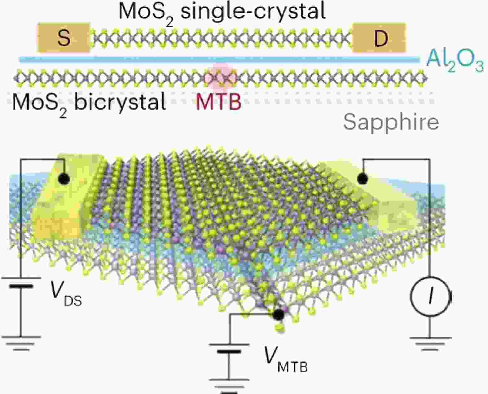
Use of the epitaxial MTBs as a 1D gate (Lg = 0.4 nm) for the construction of scaling down two-dimensional field-effect transistors
Youla Yang, Daixuan Wu, He Tian, Tian-Ling Ren
J. Semicond.  2024, 45(10): 100401  doi: 10.1088/1674-4926/24070013

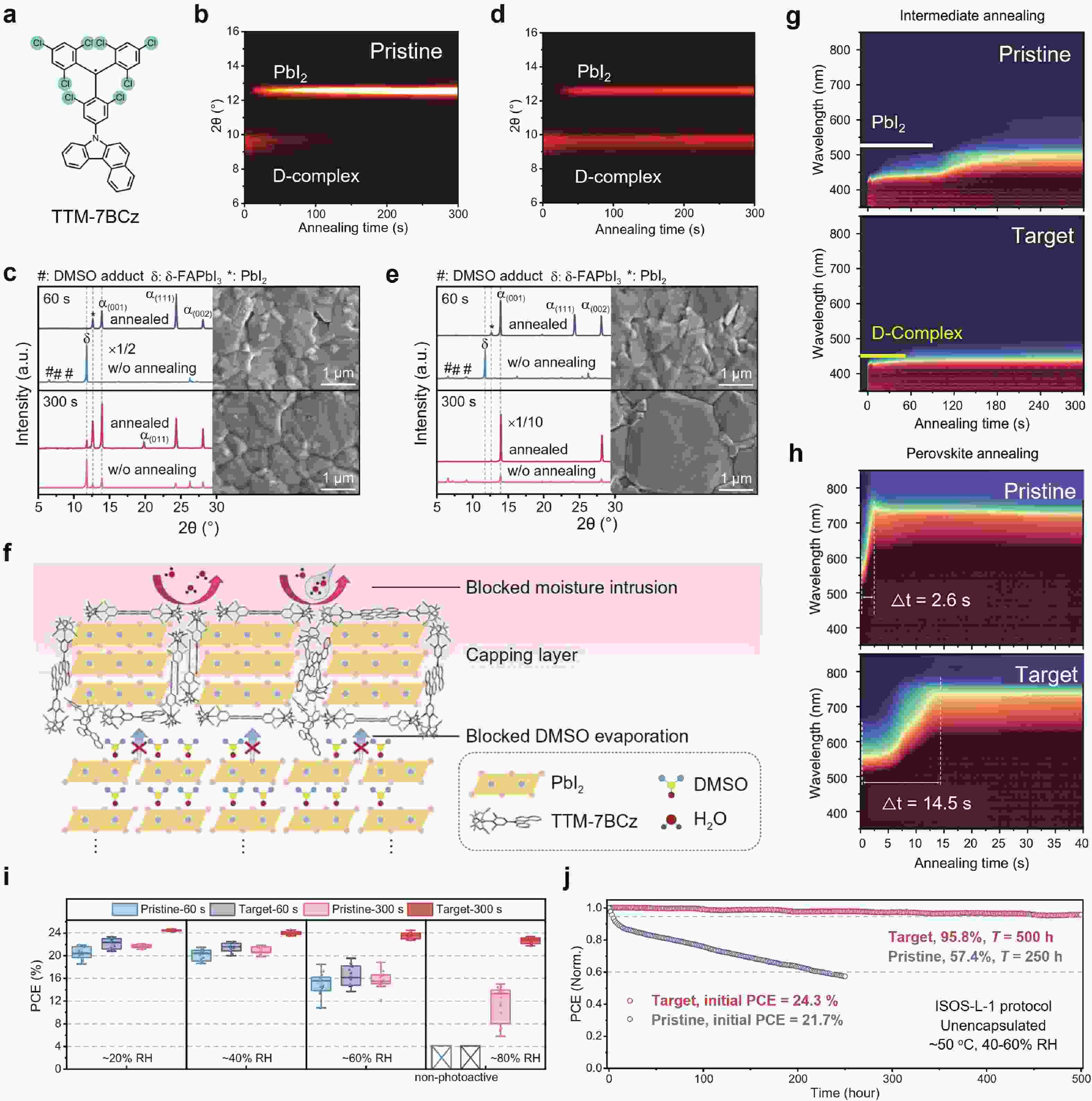
A magic organic molecule assembled capping layer enables air-processed α-FAPbI3 perovskite solar cell with state-of-the-art performances
Yulong Wang, Xiuwen Xu, Shujuan Liu, Qiang Zhao
J. Semicond.  2024, 45(10): 100402  doi: 10.1088/1674-4926/24070017

REVIEWS
A review of ToF-based LiDAR
Jie Ma, Shenglong Zhuo, Lei Qiu, Yuzhu Gao, Yifan Wu, Ming Zhong, Rui Bai, Miao Sun, Patrick Yin Chiang
J. Semicond.  2024, 45(10): 101201  doi: 10.1088/1674-4926/24040015

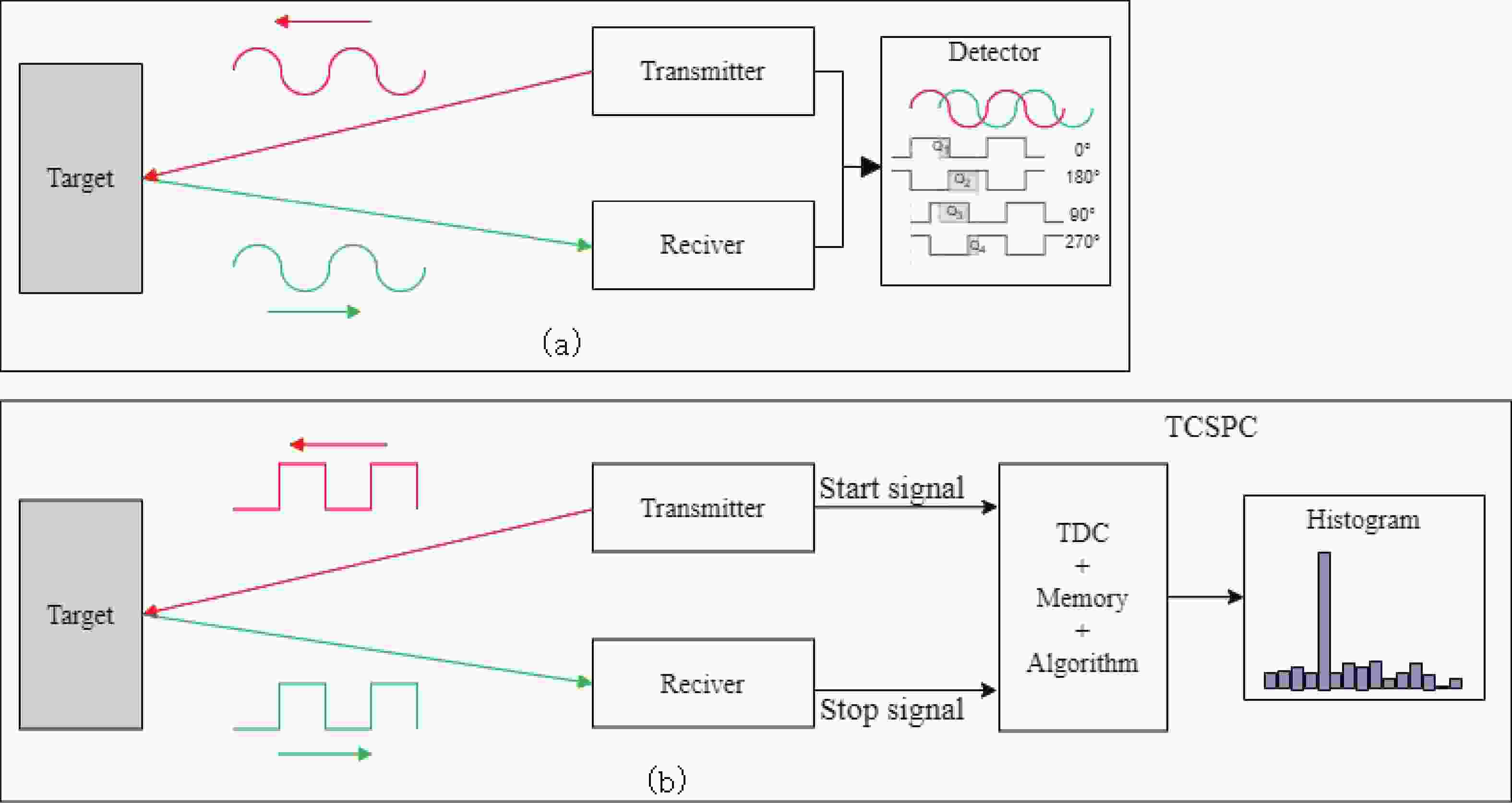
In recent years, propelled by the rapid iterative advancements in digital imaging technology and the semiconductor industry, encompassing microelectronic design, manufacturing, packaging, and testing, time-of-flight (ToF)-based imaging systems for acquiring depth information have garnered considerable attention from both academia and industry. This technology has emerged as a focal point of research within the realm of 3D imaging. Owing to its relatively straightforward principles and exceptional performance, ToF technology finds extensive applications across various domains including human−computer interaction, autonomous driving, industrial inspection, medical and healthcare, augmented reality, smart homes, and 3D reconstruction, among others. Notably, the increasing maturity of ToF-based LiDAR systems is evident in current developments. This paper comprehensively reviews the fundamental principles of ToF technology and LiDAR systems, alongside recent research advancements. It elucidates the innovative aspects and technical challenges encountered in both transmitter (TX) and receiver (RX), providing detailed discussions on corresponding solutions. Furthermore, the paper explores prospective avenues for future research, offering valuable insights for subsequent investigations.
In recent years, propelled by the rapid iterative advancements in digital imaging technology and the semiconductor industry, encompassing microelectronic design, manufacturing, packaging, and testing, time-of-flight (ToF)-based imaging systems for acquiring depth information have garnered considerable attention from both academia and industry. This technology has emerged as a focal point of research within the realm of 3D imaging. Owing to its relatively straightforward principles and exceptional performance, ToF technology finds extensive applications across various domains including human−computer interaction, autonomous driving, industrial inspection, medical and healthcare, augmented reality, smart homes, and 3D reconstruction, among others. Notably, the increasing maturity of ToF-based LiDAR systems is evident in current developments. This paper comprehensively reviews the fundamental principles of ToF technology and LiDAR systems, alongside recent research advancements. It elucidates the innovative aspects and technical challenges encountered in both transmitter (TX) and receiver (RX), providing detailed discussions on corresponding solutions. Furthermore, the paper explores prospective avenues for future research, offering valuable insights for subsequent investigations.
The exchange interaction between neighboring quantum dots: physics and applications in quantum information processing
Zheng Zhou, Yixin Li, Zhiyuan Wu, Xinping Ma, Shichang Fan, Shaoyun Huang
J. Semicond.  2024, 45(10): 101701  doi: 10.1088/1674-4926/24050043

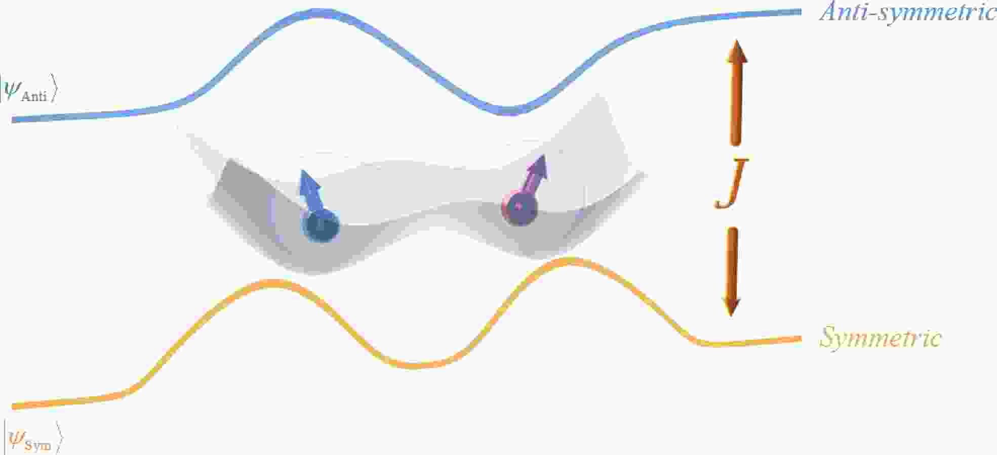
Electron spins confined in semiconductor quantum dots (QDs) are one of potential candidates for physical implementation of scalable quantum information processing technologies. Tunnel coupling based inter exchange interaction between QDs is crucial in achieving single-qubit manipulation, two-qubit gate, quantum communication and quantum simulation. This review first provides a theoretical perspective that surveys a general framework, including the Helter−London approach, the Hund−Mulliken approach, and the Hubbard model, to describe the inter exchange interactions between semiconductor quantum dots. An electrical method to control the inter exchange interaction in a realistic device is proposed as well. Then the significant achievements of inter exchange interaction in manipulating single qubits, achieving two-qubit gates, performing quantum communication and quantum simulation are reviewed. The last part is a summary of this review.
Electron spins confined in semiconductor quantum dots (QDs) are one of potential candidates for physical implementation of scalable quantum information processing technologies. Tunnel coupling based inter exchange interaction between QDs is crucial in achieving single-qubit manipulation, two-qubit gate, quantum communication and quantum simulation. This review first provides a theoretical perspective that surveys a general framework, including the Helter−London approach, the Hund−Mulliken approach, and the Hubbard model, to describe the inter exchange interactions between semiconductor quantum dots. An electrical method to control the inter exchange interaction in a realistic device is proposed as well. Then the significant achievements of inter exchange interaction in manipulating single qubits, achieving two-qubit gates, performing quantum communication and quantum simulation are reviewed. The last part is a summary of this review.
ARTICLES
Impact of strain relaxation on the growth rate of heteroepitaxial germanium tin binary alloy
Pedram Jahandar, Maksym Myronov
J. Semicond.  2024, 45(10): 102101  doi: 10.1088/1674-4926/24030002

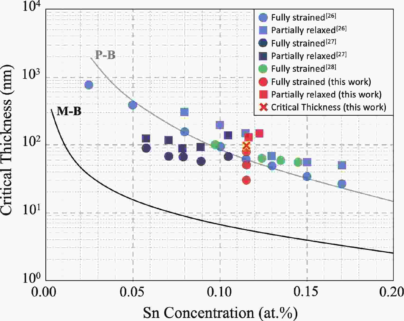
The growth of high-quality germanium tin (Ge1–ySny) binary alloys on a Si substrate using chemical vapor deposition (CVD) techniques holds immense potential for advancing electronics and optoelectronics applications, including the development of efficient and low-cost mid-infrared detectors and light sources. However, achieving precise control over the Sn concentration and strain relaxation of the Ge1–ySny epilayer, which directly influence its optical and electrical properties, remain a significant challenge. In this research, the effect of strain relaxation on the growth rate of Ge1–ySny epilayers, with Sn concentration >11at.%, is investigated. It is successfully demonstrated that the growth rate slows down by ~55% due to strain relaxation after passing its critical thickness, which suggests a reduction in the incorporation of Ge into Ge1–ySny growing layers. Despite the increase in Sn concentration as a result of the decrease in the growth rate, it has been found that the Sn incorporation rate into Ge1–ySny growing layers has also decreased due to strain relaxation. Such valuable insights could offer a foundation for the development of innovative growth techniques aimed at achieving high-quality Ge1–ySny epilayers with tuned Sn concentration and strain relaxation.
The growth of high-quality germanium tin (Ge1–ySny) binary alloys on a Si substrate using chemical vapor deposition (CVD) techniques holds immense potential for advancing electronics and optoelectronics applications, including the development of efficient and low-cost mid-infrared detectors and light sources. However, achieving precise control over the Sn concentration and strain relaxation of the Ge1–ySny epilayer, which directly influence its optical and electrical properties, remain a significant challenge. In this research, the effect of strain relaxation on the growth rate of Ge1–ySny epilayers, with Sn concentration >11at.%, is investigated. It is successfully demonstrated that the growth rate slows down by ~55% due to strain relaxation after passing its critical thickness, which suggests a reduction in the incorporation of Ge into Ge1–ySny growing layers. Despite the increase in Sn concentration as a result of the decrease in the growth rate, it has been found that the Sn incorporation rate into Ge1–ySny growing layers has also decreased due to strain relaxation. Such valuable insights could offer a foundation for the development of innovative growth techniques aimed at achieving high-quality Ge1–ySny epilayers with tuned Sn concentration and strain relaxation.
SSA-over-array (SSoA): A stacked DRAM architecture for near-memory computing
Xiping Jiang, Fujun Bai, Song Wang, Yixin Guo, Fengguo Zuo, Wenwu Xiao, Yubing Wang, Jianguo Yang, Ming Liu
J. Semicond.  2024, 45(10): 102201  doi: 10.1088/1674-4926/24050004

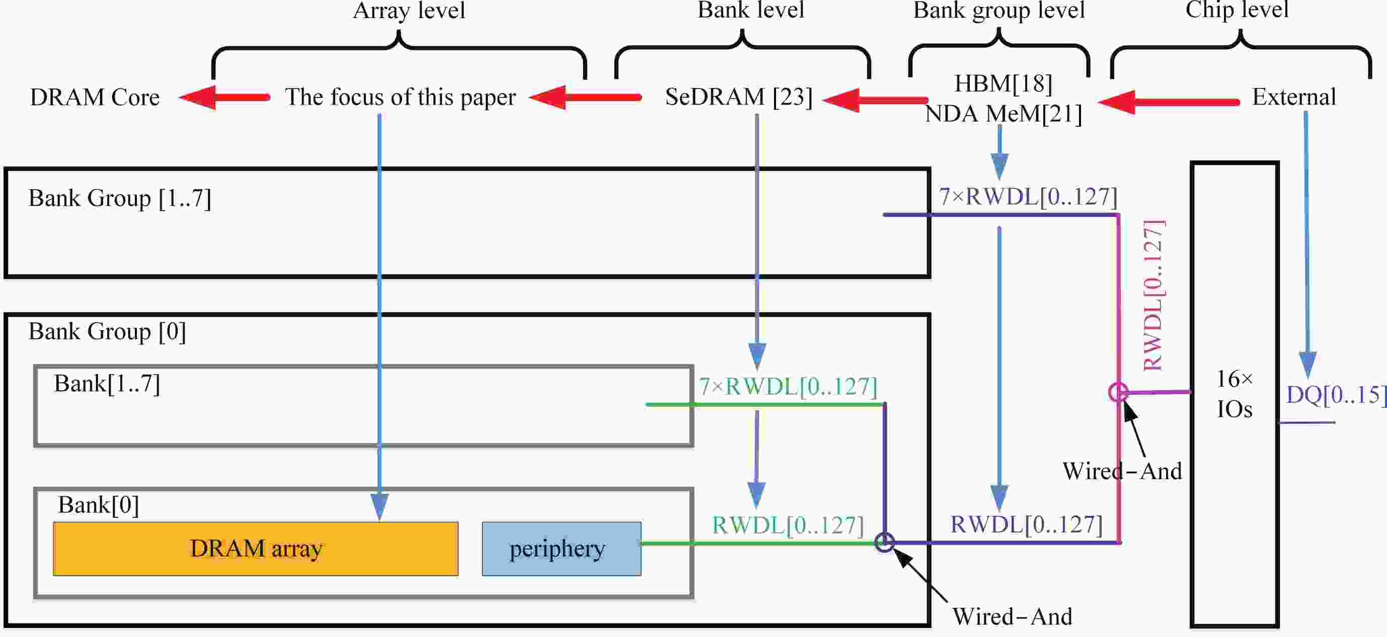
Aiming to enhance the bandwidth in near-memory computing, this paper proposes a SSA-over-array (SSoA) architecture. By relocating the secondary sense amplifier (SSA) from dynamic random access memory (DRAM) to the logic die and repositioning the DRAM-to-logic stacking interface closer to the DRAM core, the SSoA overcomes the layout and area limitations of SSA and master DQ (MDQ), leading to improvements in DRAM data-width density and frequency, significantly enhancing bandwidth density. The quantitative evaluation results show a 70.18 times improvement in bandwidth per unit area over the baseline, with a maximum bandwidth of 168.296 Tbps/Gb. We believe the SSoA is poised to redefine near-memory computing development strategies.
Aiming to enhance the bandwidth in near-memory computing, this paper proposes a SSA-over-array (SSoA) architecture. By relocating the secondary sense amplifier (SSA) from dynamic random access memory (DRAM) to the logic die and repositioning the DRAM-to-logic stacking interface closer to the DRAM core, the SSoA overcomes the layout and area limitations of SSA and master DQ (MDQ), leading to improvements in DRAM data-width density and frequency, significantly enhancing bandwidth density. The quantitative evaluation results show a 70.18 times improvement in bandwidth per unit area over the baseline, with a maximum bandwidth of 168.296 Tbps/Gb. We believe the SSoA is poised to redefine near-memory computing development strategies.
Heterojunction-engineered carrier transport in elevated-metal metal-oxide thin-film transistors
Xiao Li, Zhikang Ma, Jinxiong Li, Wengao Pan, Congwei Liao, Shengdong Zhang, Zhuo Gao, Dong Fu, Lei Lu
J. Semicond.  2024, 45(10): 102301  doi: 10.1088/1674-4926/24040016

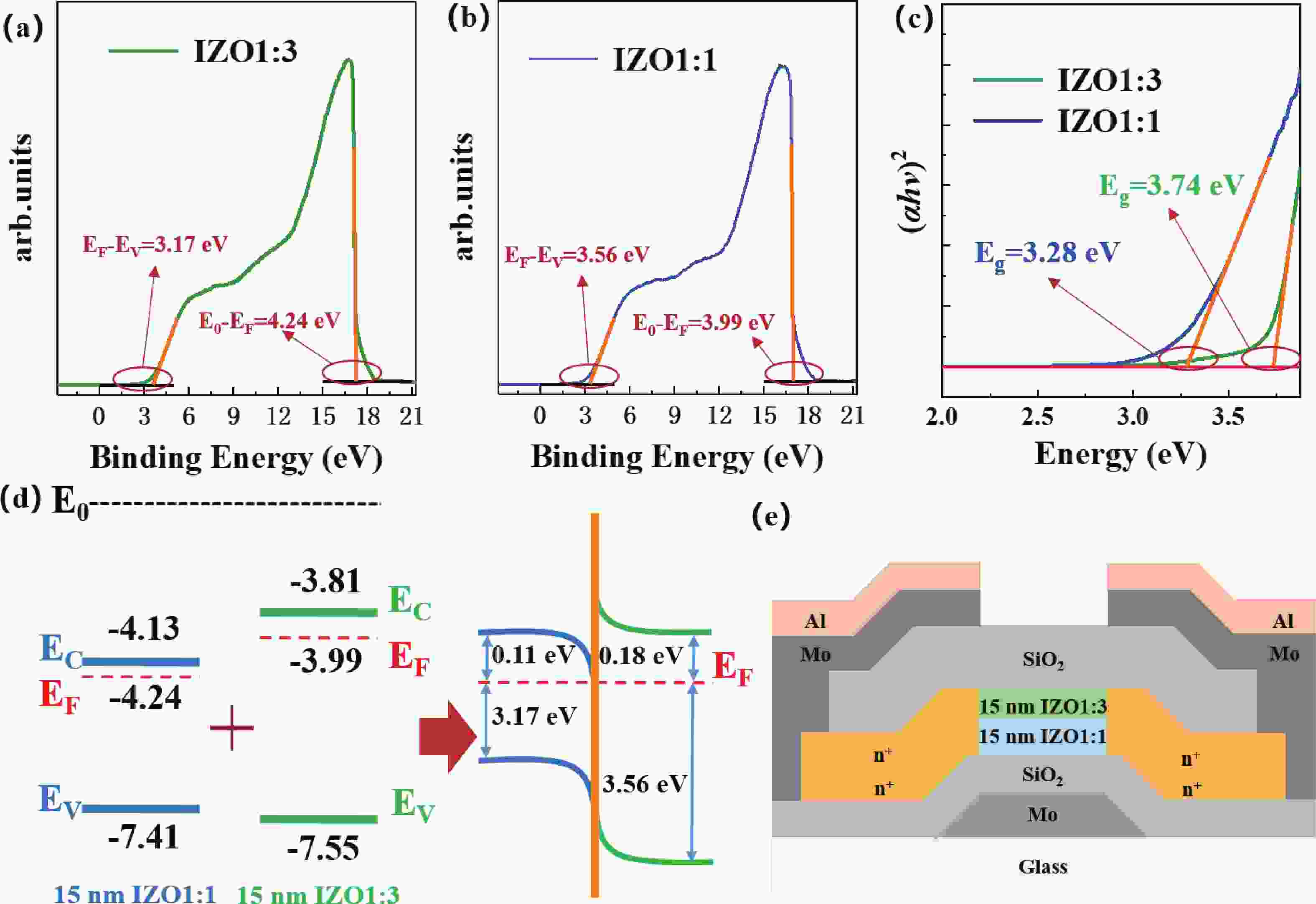
This study investigates the carrier transport of heterojunction channel in oxide semiconductor thin-film transistor (TFT) using the elevated-metal metal-oxide (EMMO) architecture and indium−zinc oxide (InZnO). The heterojunction band diagram of InZnO bilayer was modified by the cation composition to form the two-dimensional electron gas (2DEG) at the interface quantum well, as verified using a metal−insulator−semiconductor (MIS) device. Although the 2DEG indeed contributes to a higher mobility than the monolayer channel, the competition and cooperation between the gate field and the built-in field strongly affect such mobility-boosting effect, originating from the carrier inelastic collision at the heterojunction interface and the gate field-induced suppression of quantum well. Benefited from the proper energy-band engineering, a high mobility of 84.3 cm2·V−1·s−1, a decent threshold voltage (Vth) of −6.5 V, and a steep subthreshold swing (SS) of 0.29 V/dec were obtained in InZnO-based heterojunction TFT.
This study investigates the carrier transport of heterojunction channel in oxide semiconductor thin-film transistor (TFT) using the elevated-metal metal-oxide (EMMO) architecture and indium−zinc oxide (InZnO). The heterojunction band diagram of InZnO bilayer was modified by the cation composition to form the two-dimensional electron gas (2DEG) at the interface quantum well, as verified using a metal−insulator−semiconductor (MIS) device. Although the 2DEG indeed contributes to a higher mobility than the monolayer channel, the competition and cooperation between the gate field and the built-in field strongly affect such mobility-boosting effect, originating from the carrier inelastic collision at the heterojunction interface and the gate field-induced suppression of quantum well. Benefited from the proper energy-band engineering, a high mobility of 84.3 cm2·V−1·s−1, a decent threshold voltage (Vth) of −6.5 V, and a steep subthreshold swing (SS) of 0.29 V/dec were obtained in InZnO-based heterojunction TFT.
Structure and electrical properties of polysilicon films doped with ammonium tetraborate tetrahydrate
Yehua Tang, Yuchao Wang, Chunlan Zhou, Ke-Fan Wang
J. Semicond.  2024, 45(10): 102302  doi: 10.1088/1674-4926/24030032

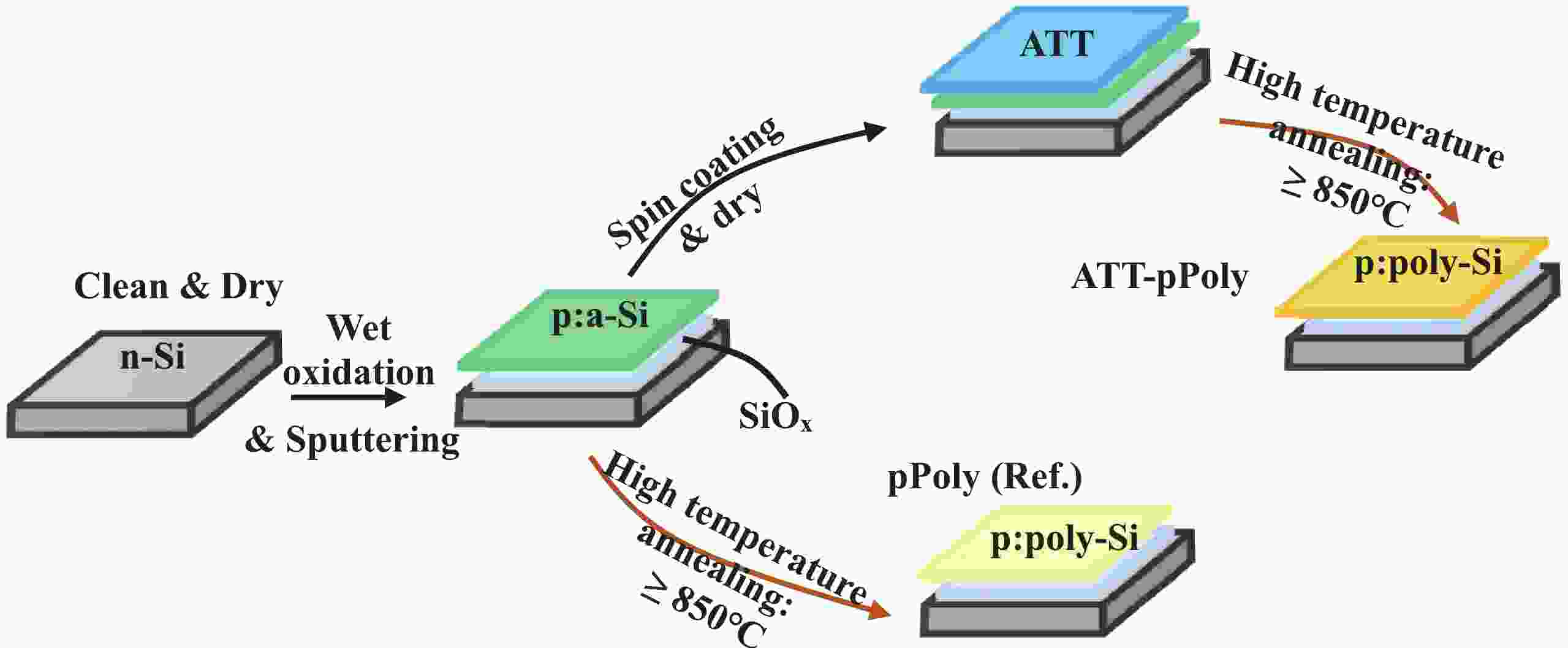
Here, p-type polysilicon films are fabricated by ex-situ doping method with ammonium tetraborate tetrahydrate (ATT) as the boron source, named ATT-pPoly. The effects of ATT on the properties of polysilicon films are comprehensively analyzed. The Raman spectra reveal that the ATT-pPoly film is composed of grain boundary and crystalline regions. The preferred orientation is the (111) direction. The grain size increases from 16−23 nm to 21−47 nm, by ~70% on average. Comparing with other reported films, Hall measurements reveal that the ATT-pPoly film has a higher carrier concentration (>1020 cm−3) and higher carrier mobility (>30 cm2/(V·s)). The superior properties of the ATT-pPoly film are attributed to the heavy doping and improved grain size. Heavy doping property is proved by the mean sheet resistance (Rsheet,m) and distribution profile. The Rsheet,m decreases by more than 30%, and it can be further decreased by 90% if the annealing temperature or duration is increased. The boron concentration of ATT-pPoly film annealed at 950 °C for 45 min is ~3 × 1020 cm−3, and the distribution is nearly the same, except near the surface. Besides, the standard deviation coefficient (σ) of Rsheet,m is less than 5.0%, which verifies the excellent uniformity of ATT-pPoly film.

Here, p-type polysilicon films are fabricated by ex-situ doping method with ammonium tetraborate tetrahydrate (ATT) as the boron source, named ATT-pPoly. The effects of ATT on the properties of polysilicon films are comprehensively analyzed. The Raman spectra reveal that the ATT-pPoly film is composed of grain boundary and crystalline regions. The preferred orientation is the (111) direction. The grain size increases from 16−23 nm to 21−47 nm, by ~70% on average. Comparing with other reported films, Hall measurements reveal that the ATT-pPoly film has a higher carrier concentration (>1020 cm−3) and higher carrier mobility (>30 cm2/(V·s)). The superior properties of the ATT-pPoly film are attributed to the heavy doping and improved grain size. Heavy doping property is proved by the mean sheet resistance (Rsheet,m) and distribution profile. The Rsheet,m decreases by more than 30%, and it can be further decreased by 90% if the annealing temperature or duration is increased. The boron concentration of ATT-pPoly film annealed at 950 °C for 45 min is ~3 × 1020 cm−3, and the distribution is nearly the same, except near the surface. Besides, the standard deviation coefficient (σ) of Rsheet,m is less than 5.0%, which verifies the excellent uniformity of ATT-pPoly film.
Single-fundamental-mode cryogenic (3.6 K) 850-nm oxide-confined VCSEL
Anjin Liu, Chenxi Hao, Jingyu Huo, Hailong Han, Minglu Wang, Bao Tang, Lingyun Li, Lixing You, Wanhua Zheng
J. Semicond.  2024, 45(10): 102401  doi: 10.1088/1674-4926/24070025

Cryogenic oxide-confined vertical-cavity surface-emitting laser (VCSEL) has promising application in cryogenic optical interconnect for cryogenic computing. In this paper, we demonstrate a cryogenic 850-nm oxide-confined VCSEL at around 4 K. The cryogenic VCSEL with an optical oxide aperture of 6.5 μm in diameter can operate in single fundamental mode with a side-mode suppression-ratio of 36 dB at 3.6 K, and the fiber-coupled output power reaches 1 mW at 5 mA. The small signal modulation measurements at 298 and 292 K show the fabricated VCSEL has the potential to achieve a high modulation bandwidth at cryogenic temperature.
Cryogenic oxide-confined vertical-cavity surface-emitting laser (VCSEL) has promising application in cryogenic optical interconnect for cryogenic computing. In this paper, we demonstrate a cryogenic 850-nm oxide-confined VCSEL at around 4 K. The cryogenic VCSEL with an optical oxide aperture of 6.5 μm in diameter can operate in single fundamental mode with a side-mode suppression-ratio of 36 dB at 3.6 K, and the fiber-coupled output power reaches 1 mW at 5 mA. The small signal modulation measurements at 298 and 292 K show the fabricated VCSEL has the potential to achieve a high modulation bandwidth at cryogenic temperature.
Improved efficiency and stability of inverse perovskite solar cells via passivation cleaning
Kunyang Ge, Chunjun Liang
J. Semicond.  2024, 45(10): 102801  doi: 10.1088/1674-4926/24040033

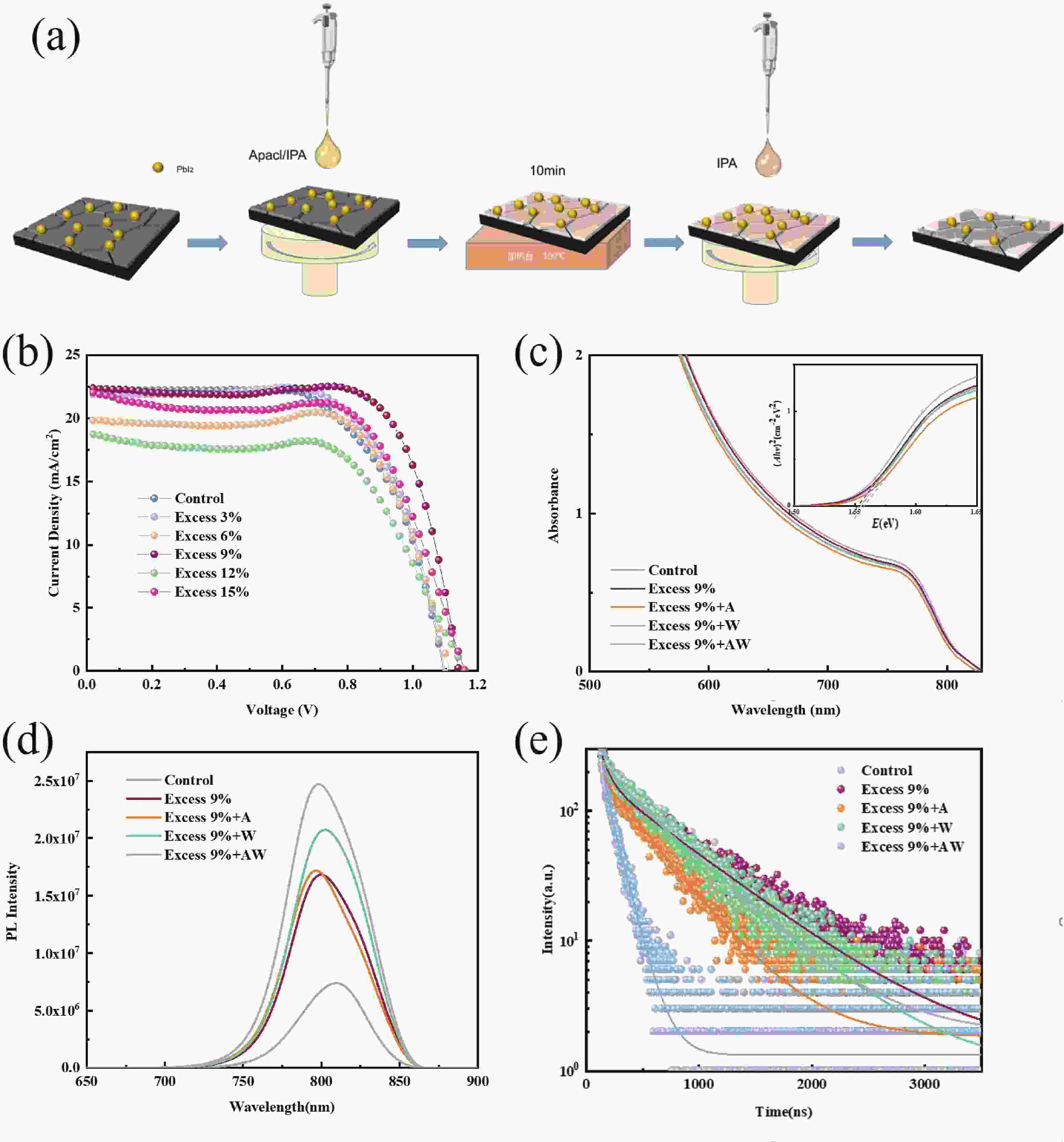
Amidst the global energy and environmental crisis, the quest for efficient solar energy utilization intensifies. Perovskite solar cells, with efficiencies over 26% and cost-effective production, are at the forefront of research. Yet, their stability remains a barrier to industrial application. This study introduces innovative strategies to enhance the stability of inverted perovskite solar cells. By bulk and surface passivation, defect density is reduced, followed by a "passivation cleaning" using Apacl amino acid salt and isopropyl alcohol to refine film surface quality. Employing X-ray diffraction (XRD), scanning electron microscope (SEM), and atomic force microscopy (AFM), we confirmed that this process effectively neutralizes surface defects and curbs non-radiative recombination, achieving 22.6% efficiency for perovskite solar cells with the composition Cs0.15FA0.85PbI3. Crucially, the stability of treated cells in long-term tests has been markedly enhanced, laying groundwork for industrial viability.
Amidst the global energy and environmental crisis, the quest for efficient solar energy utilization intensifies. Perovskite solar cells, with efficiencies over 26% and cost-effective production, are at the forefront of research. Yet, their stability remains a barrier to industrial application. This study introduces innovative strategies to enhance the stability of inverted perovskite solar cells. By bulk and surface passivation, defect density is reduced, followed by a "passivation cleaning" using Apacl amino acid salt and isopropyl alcohol to refine film surface quality. Employing X-ray diffraction (XRD), scanning electron microscope (SEM), and atomic force microscopy (AFM), we confirmed that this process effectively neutralizes surface defects and curbs non-radiative recombination, achieving 22.6% efficiency for perovskite solar cells with the composition Cs0.15FA0.85PbI3. Crucially, the stability of treated cells in long-term tests has been markedly enhanced, laying groundwork for industrial viability.
The surface electron transfer strategy promotes the hole of PDI release and enhances emerging organic pollutant degradation
Yunchuan Yang, Dongyu Wang, Jisheng Geng, Jun Liu, Jun Wang
J. Semicond.  2024, 45(10): 102802  doi: 10.1088/1674-4926/24050005

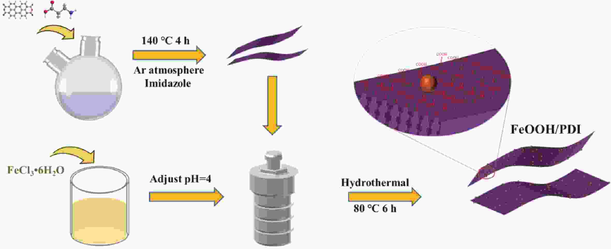
In semiconductor photocatalysts, the easy recombination of photogenerated carriers seriously affects the application of photocatalytic materials in water treatment. To solve the serious problem of electron−hole pair recombination in perylene diimide (PDI) organic semiconductors, we loaded ferric hydroxyl oxide (FeOOH) on PDI materials, successfully prepared novel FeOOH@PDI photocatalytic materials, and constructed a photo-Fenton system. The system was able to achieve highly efficient degradation of BPA under visible light, with a degradation rate of 0.112 min−1 that was 20 times higher than the PDI system, and it also showed universal degradation performances for a variety of emerging organic pollutants and anti-interference ability. The mechanism research revealed that the FeOOH has the electron trapping property, which can capture the photogenerated electrons on the surface of PDI, effectively reducing the compounding rate of photogenerated carriers of PDI and accelerating the iron cycling and H2O2 activation on the surface of FeOOH at the same time. This work provides new insights and methods for solving the problem of easy recombination of carriers in semiconductor photocatalysts and degrading emerging organic pollutants.

In semiconductor photocatalysts, the easy recombination of photogenerated carriers seriously affects the application of photocatalytic materials in water treatment. To solve the serious problem of electron−hole pair recombination in perylene diimide (PDI) organic semiconductors, we loaded ferric hydroxyl oxide (FeOOH) on PDI materials, successfully prepared novel FeOOH@PDI photocatalytic materials, and constructed a photo-Fenton system. The system was able to achieve highly efficient degradation of BPA under visible light, with a degradation rate of 0.112 min−1 that was 20 times higher than the PDI system, and it also showed universal degradation performances for a variety of emerging organic pollutants and anti-interference ability. The mechanism research revealed that the FeOOH has the electron trapping property, which can capture the photogenerated electrons on the surface of PDI, effectively reducing the compounding rate of photogenerated carriers of PDI and accelerating the iron cycling and H2O2 activation on the surface of FeOOH at the same time. This work provides new insights and methods for solving the problem of easy recombination of carriers in semiconductor photocatalysts and degrading emerging organic pollutants.