| Citation: |
Yehua Tang, Yuchao Wang, Chunlan Zhou, Ke-Fan Wang. Structure and electrical properties of polysilicon films doped with ammonium tetraborate tetrahydrate[J]. Journal of Semiconductors, 2024, 45(10): 102302. doi: 10.1088/1674-4926/24030032
****
Y H Tang, Y C Wang, C L Zhou, and K F Wang, Structure and electrical properties of polysilicon films doped with ammonium tetraborate tetrahydrate[J]. J. Semicond., 2024, 45(10), 102302 doi: 10.1088/1674-4926/24030032
|
Structure and electrical properties of polysilicon films doped with ammonium tetraborate tetrahydrate
DOI: 10.1088/1674-4926/24030032
CSTR: 32376.14.1674-4926.24030032
More Information-
Abstract
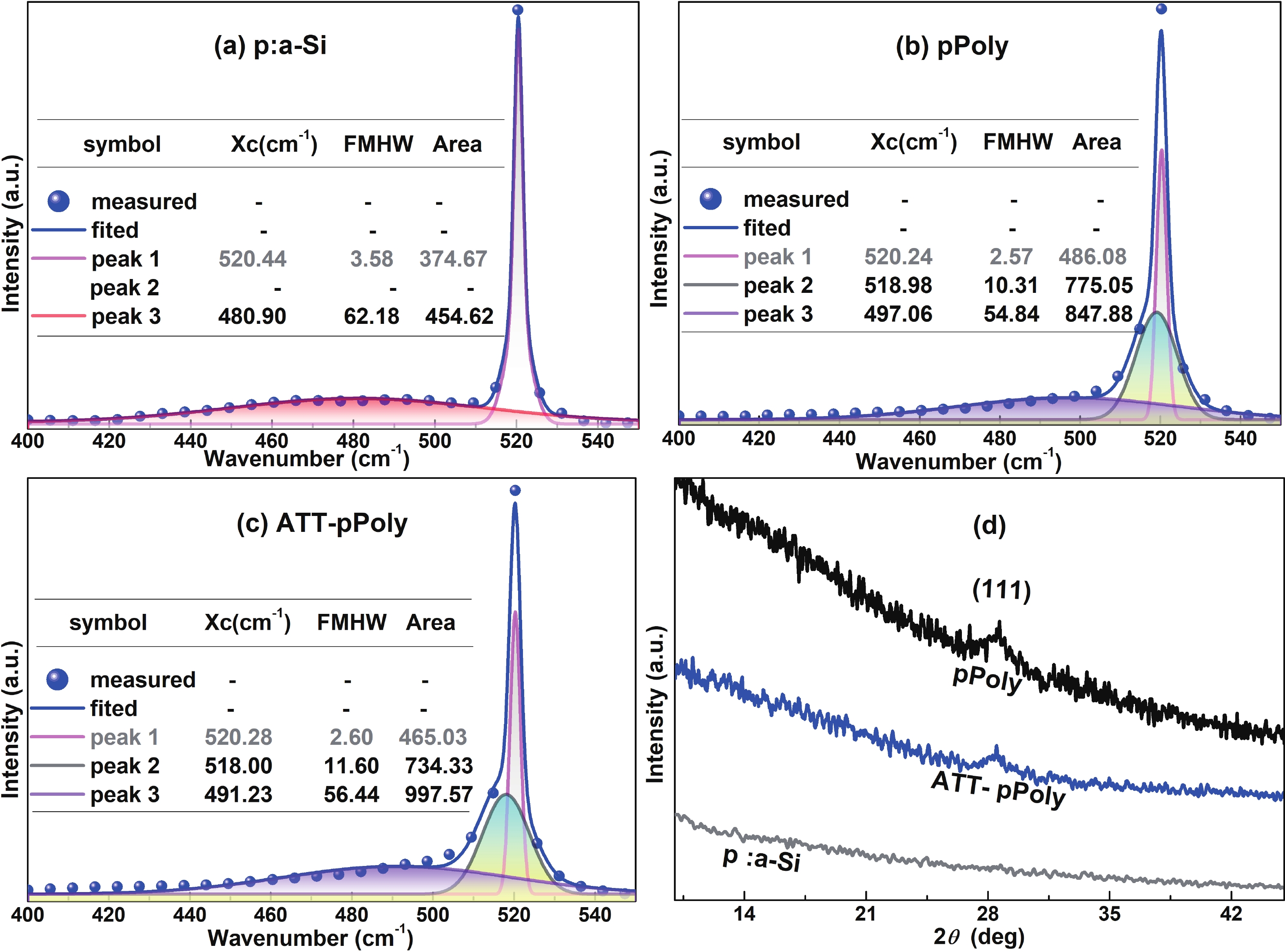
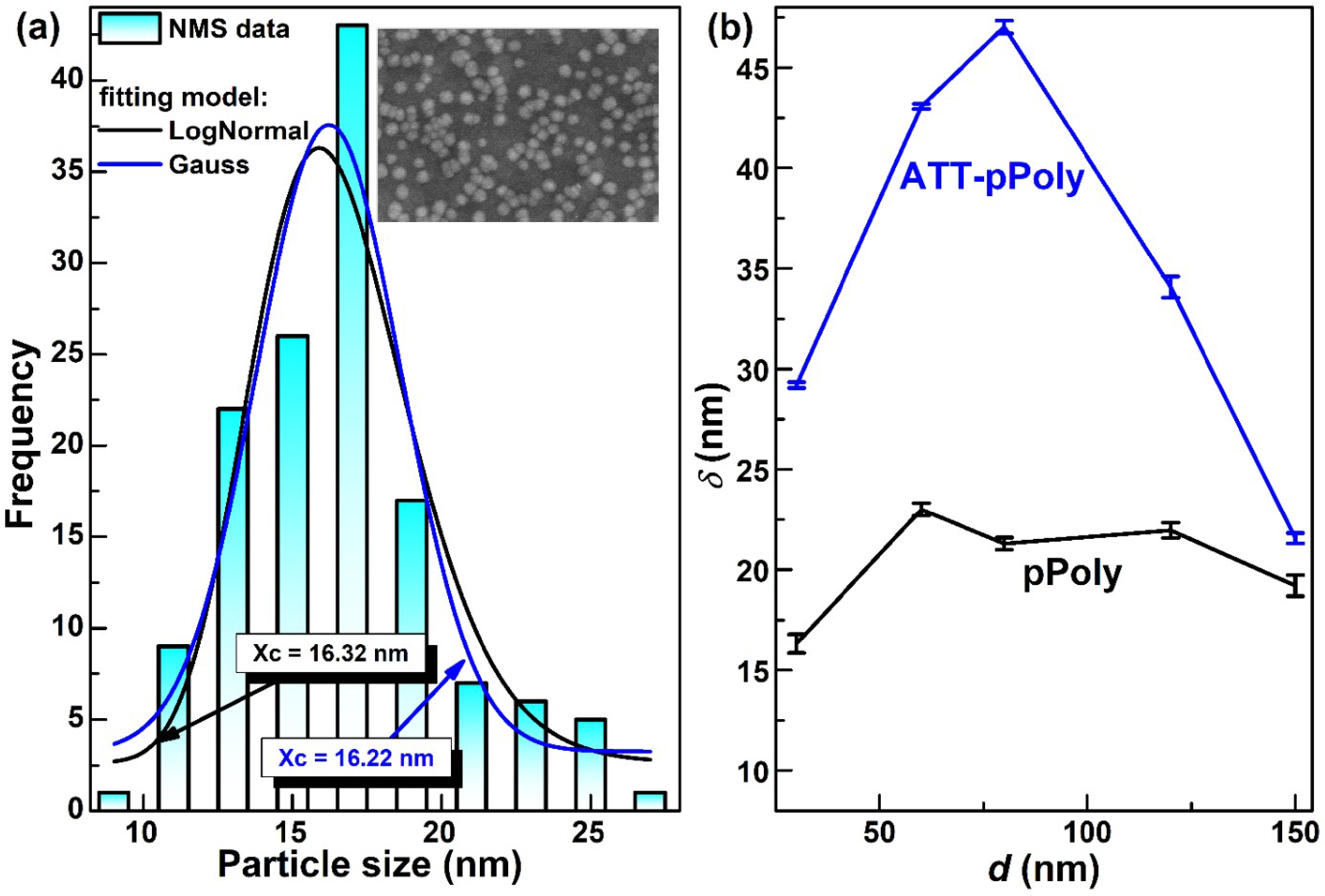
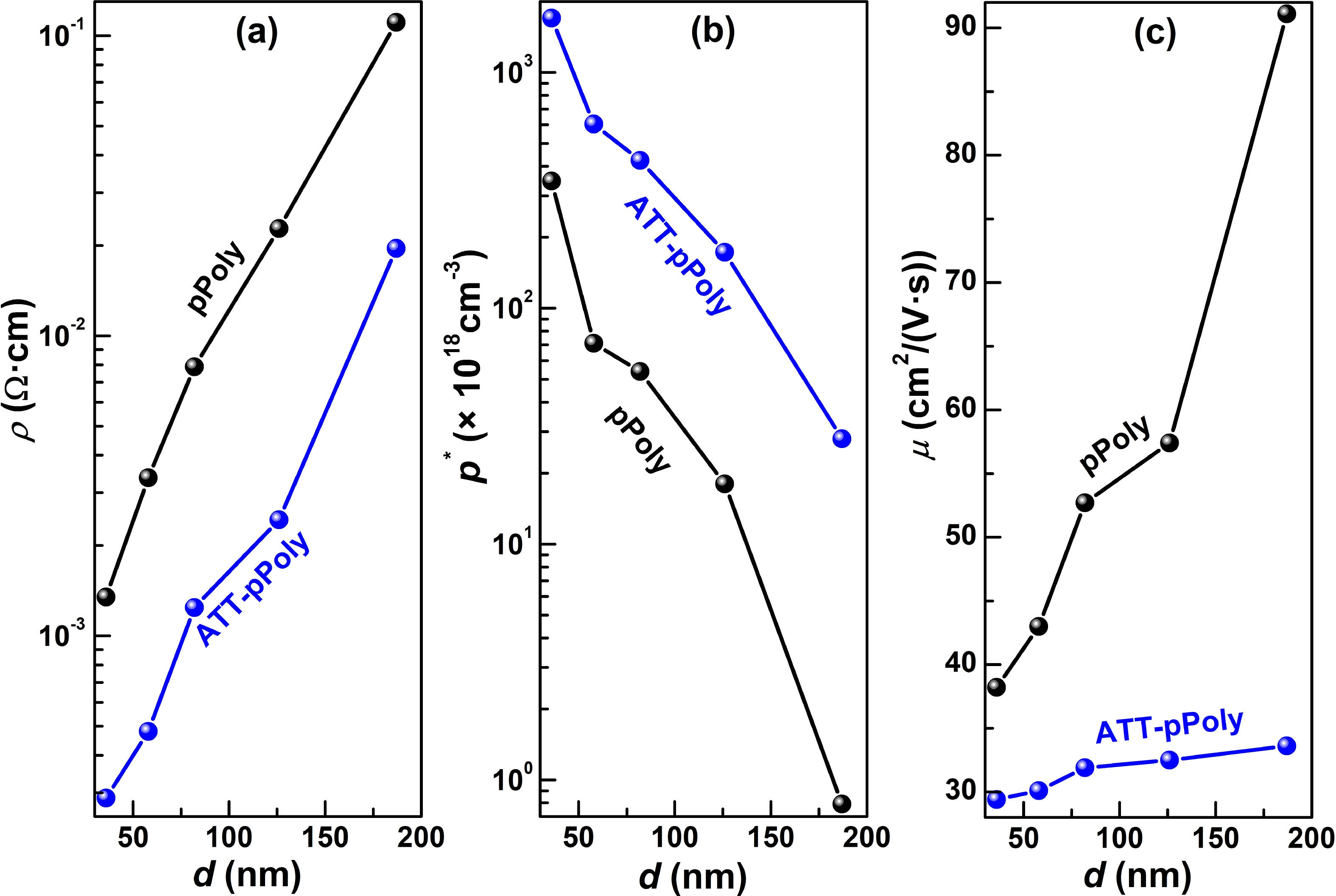
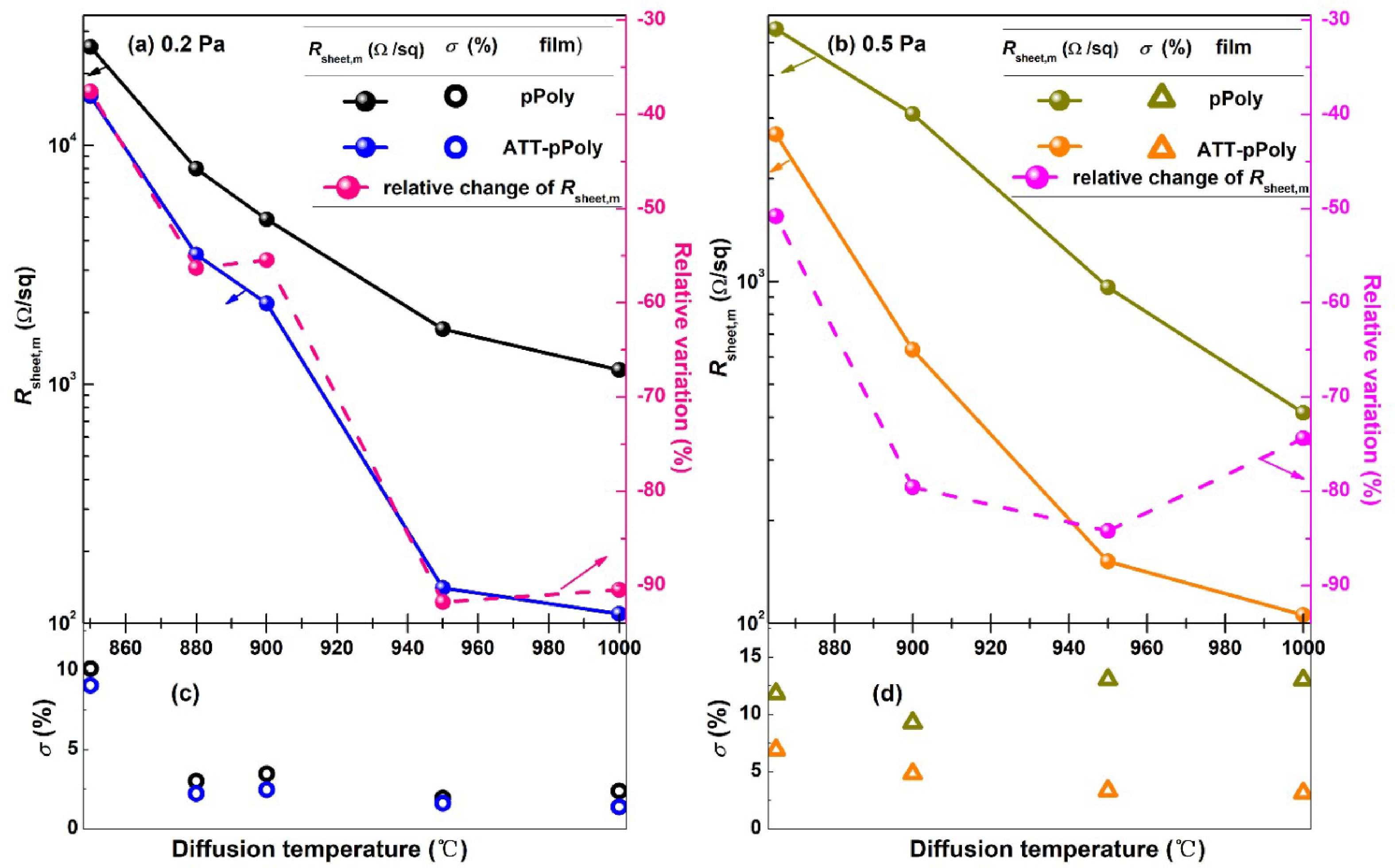
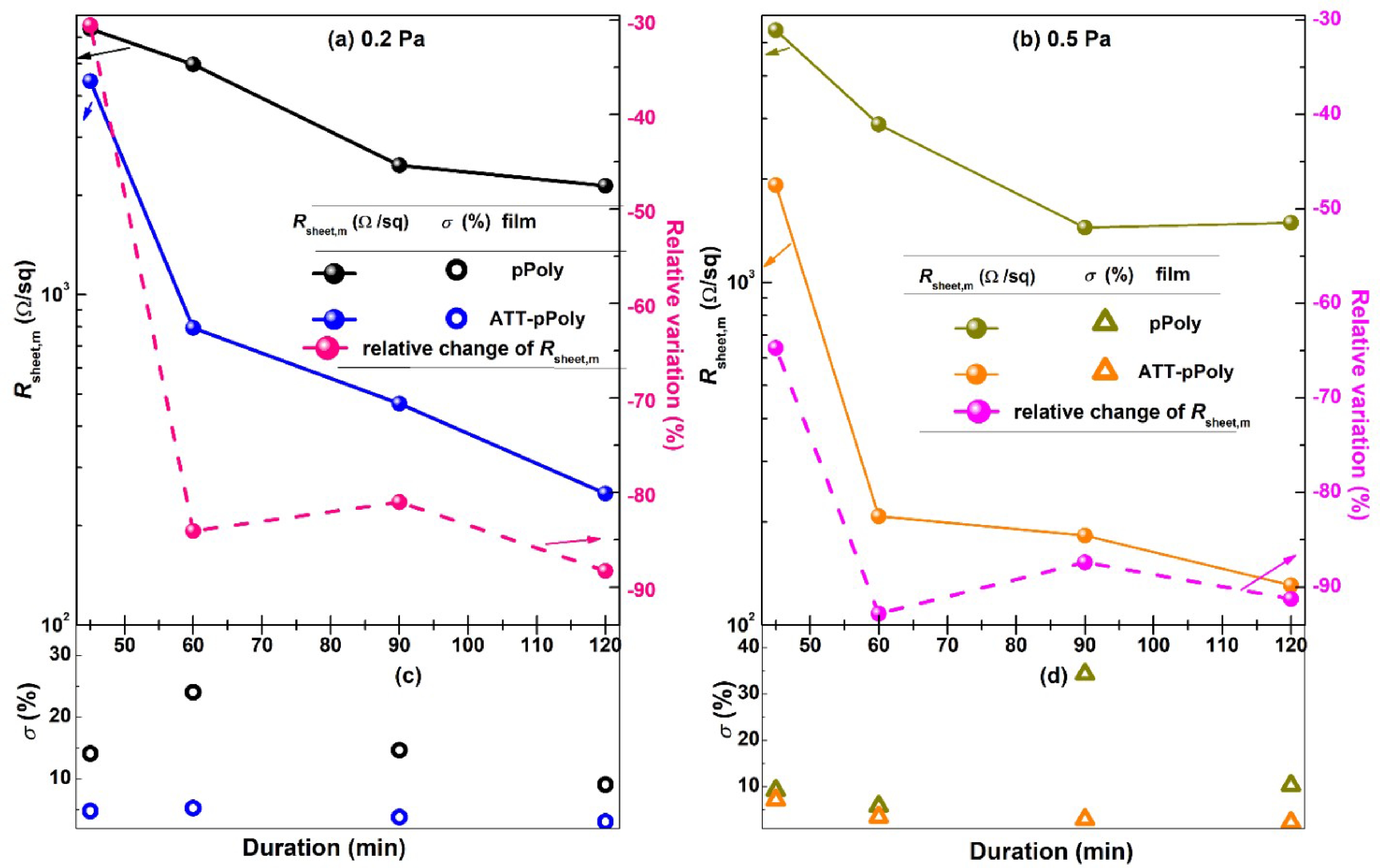
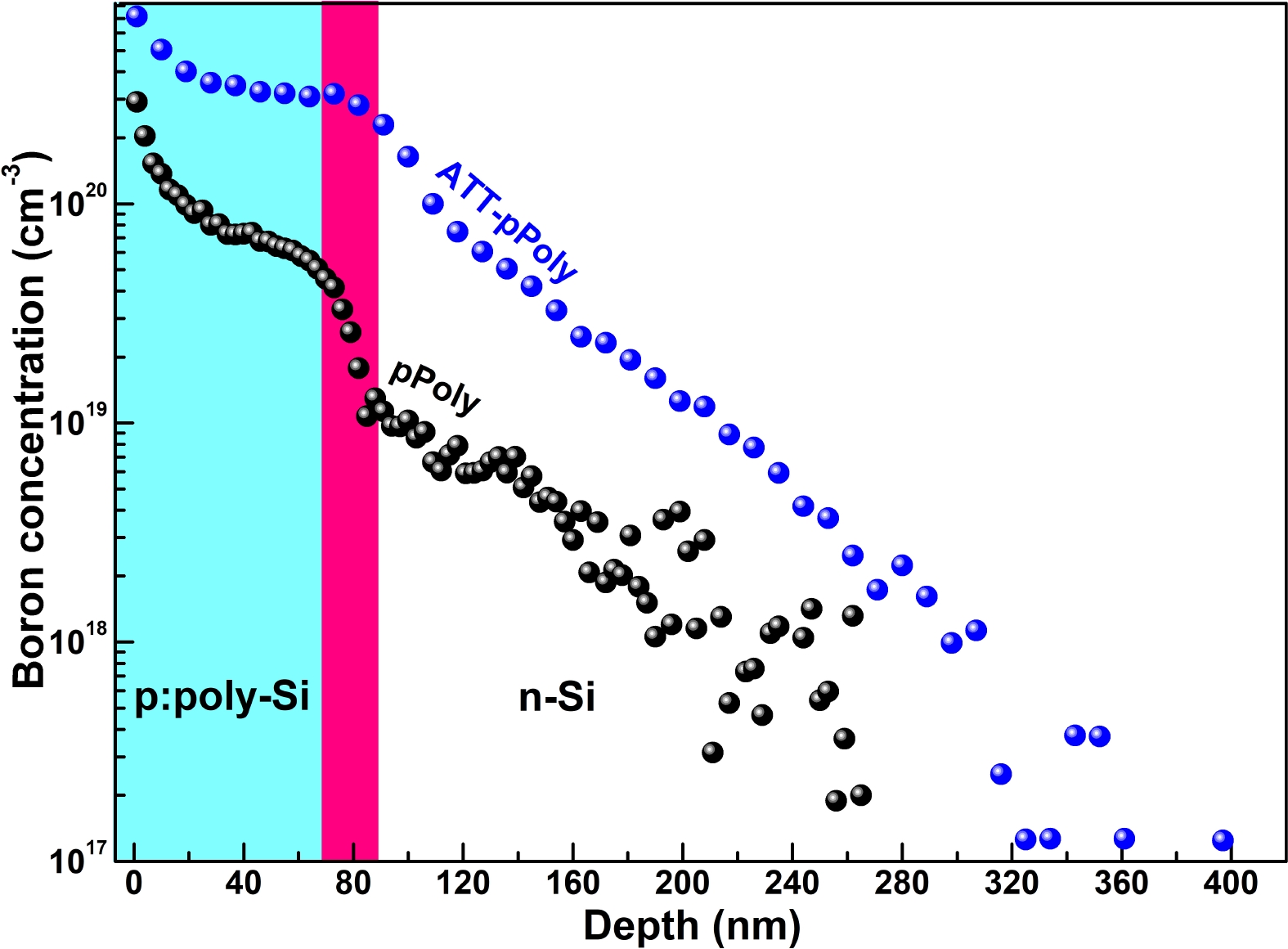
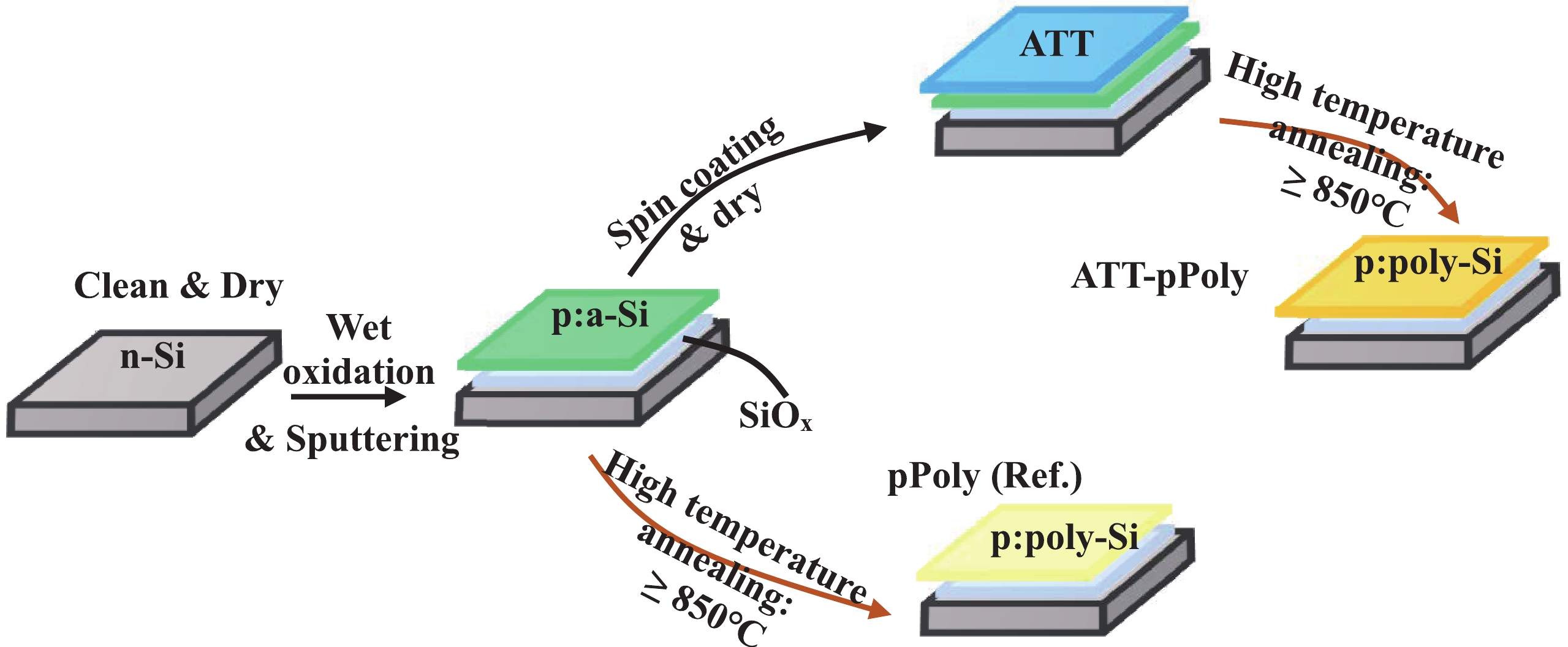
Here, p-type polysilicon films are fabricated by ex-situ doping method with ammonium tetraborate tetrahydrate (ATT) as the boron source, named ATT-pPoly. The effects of ATT on the properties of polysilicon films are comprehensively analyzed. The Raman spectra reveal that the ATT-pPoly film is composed of grain boundary and crystalline regions. The preferred orientation is the (111) direction. The grain size increases from 16−23 nm to 21−47 nm, by ~70% on average. Comparing with other reported films, Hall measurements reveal that the ATT-pPoly film has a higher carrier concentration (>1020 cm−3) and higher carrier mobility (>30 cm2/(V·s)). The superior properties of the ATT-pPoly film are attributed to the heavy doping and improved grain size. Heavy doping property is proved by the mean sheet resistance (Rsheet,m) and distribution profile. The Rsheet,m decreases by more than 30%, and it can be further decreased by 90% if the annealing temperature or duration is increased. The boron concentration of ATT-pPoly film annealed at 950 °C for 45 min is ~3 × 1020 cm−3, and the distribution is nearly the same, except near the surface. Besides, the standard deviation coefficient (σ) of Rsheet,m is less than 5.0%, which verifies the excellent uniformity of ATT-pPoly film. -
References
[1] International Technology Roadmap for Photovoltaic, 14 Edition, April 2023, http://www.itrpv.net/Reports/Downloads/[2] Augusto A, Karas J, Balaji P, et al. Exploring the practical efficiency limit of silicon solar cells using thin solar-grade substrates. J Mater Chem A, 2020, 8, 16599 doi: 10.1039/D0TA04575F[3] Ji F X, Zhou C L, Zhu J J, et al. Surface related degradation phenomena in P-type multi-crystalline silicon at elevated temperature and illumination. Sol Energy, 2020, 204, 26 doi: 10.1016/j.solener.2020.04.023[4] Le T T, Yang Z S, Liang W S, et al. Gettering of iron by aluminum oxide thin films on silicon wafers: Kinetics and mechanisms. J Appl Phys, 2024, 135, 063102 doi: 10.1063/5.0182127[5] Ding D, Lu G L, Li Z P, et al. High-efficiency n-type silicon PERT bifacial solar cells with selective emitters and poly-Si based passivating contacts. Sol Energy, 2019, 193, 494 doi: 10.1016/j.solener.2019.09.085[6] Richter A, Benick J, Feldmann F, et al. N-Type Si solar cells with passivating electron contact: Identifying sources for efficiency limitations by wafer thickness and resistivity variation. Sol Energy Mater Sol Cells, 2017, 173, 96 doi: 10.1016/j.solmat.2017.05.042[7] Richter A, Benick J, Müller R, et al. Tunnel oxide passivating electron contacts as full-area rear emitter of high-efficiency p-type silicon solar cells. Prog Photovolt Res Appl, 2017, 26, 579 doi: 10.1002/pip.2960[8] Green M A, Dunlop E D, Hohl-Ebinger J, et al. Solar cell efficiency tables (version 60). Prog Photovolt Res Appl, 2022, 30, 687 doi: 10.1002/pip.3595[9] Peibst R, Larionova Y, Reiter S, et al. Implementation of n+ and p+ poly junctions on front and rear side of double-side contacted industrial silicon solar cells. 32nd European Photovoltaic Solar Energy Conference and Exhibition, 2016, 323 doi: 10.4229/EUPVSEC20162016-2BO[10] Chen Y F, Chen D M, Liu C F, et al. Mass production of industrial tunnel oxide passivated contacts (i-TOPCon) silicon solar cells with average efficiency over 23% and modules over 345W. Prog Photovolt Res Appl, 2019, 27, 827 doi: 10.1002/pip.3180[11] Yan D, Cuevas A, Wan Y M, et al. Passivating contacts for silicon solar cells based on boron-diffused recrystallized amorphous silicon and thin dielectric interlayers. Sol Energy Mater Sol Cells, 2016, 152, 73 doi: 10.1016/j.solmat.2016.03.033[12] Gao T, Yang Q, Guo X Q, et al. An industrially viable TOPCon structure with both ultra-thin SiOx and n+-poly-Si processed by PECVD for p-type c-Si solar cells. Sol Energy Mater Sol Cells, 2019, 200, 109926 doi: 10.1016/j.solmat.2019.109926[13] Merkle A, Seren S, Knauss H, et al. Atmospheric pressure chemical vapor deposition of in-situ doped amorphous silicon layers for passivating contacts. 35th European Photovoltaic Solar Energy Conference and Exhibition, 2018, 785 doi: 10.4229/35thEUPVSEC20182018-2DV.3.49[14] Li S H, Pomaska M, Hoß J, et al. Poly-Si/SiOx/c-Si passivating contact with 738 mV implied open circuit voltage fabricated by hot-wire chemical vapor deposition. Appl Phys Lett, 2019, 114, 153901 doi: 10.1063/1.5089650[15] Li S H, Pomaska M, Hoß J, et al. In situ-doped silicon thin films for passivating contacts by hot-wire chemical vapor deposition with a high deposition rate of 42 nm/min. ACS Appl Mater Interfaces, 2019, 11, 30493 doi: 10.1021/acsami.9b10360[16] Yan D, Cuevas A, Phang S P, et al. 23% efficient p-type crystalline silicon solar cells with hole-selective passivating contacts based on physical vapor deposition of doped silicon films. Appl Phys Lett, 2018, 113, 061603 doi: 10.1063/1.5037610[17] Tao K, Jiang S, Jia R, et al. The impact of indium tin oxide deposition and post annealing on the passivation property of TOPCon solar cells. Sol Energy, 2018, 176, 241 doi: 10.1016/j.solener.2018.10.034[18] Tao Y G, Chang E L, Upadhyaya A, et al. 730 mV implied Voc enabled by tunnel oxide passivated contact with PECVD grown and crystallized n+ polycrystalline Si. 2015 IEEE 42nd Photovoltaic Specialist Conference (PVSC), 2015, 1 doi: 10.1109/PVSC.2015.7356218[19] Feldmann F, Simon M, Bivour M, et al. Carrier-selective contacts for Si solar cells. Appl Phys Lett, 2014, 104, 181105 doi: 10.1063/1.4875904[20] Park H, Park H, Park S J, et al. Passivation quality control in poly-Si/SiO x/c-Si passivated contact solar cells with 734 mV implied open circuit voltage. Sol Energy Mater Sol Cells, 2019, 189, 21 doi: 10.1016/j.solmat.2018.09.013[21] Morisset A, Cabal R, Giglia V, et al. Evolution of the surface passivation mechanism during the fabrication of ex-situ doped poly-Si(B)/SiOx passivating contacts for high-efficiency c-Si solar cells. Sol Energy Mater Sol Cells, 2021, 221, 110899 doi: 10.1016/j.solmat.2020.110899[22] Kang D, Sio H C, Stuckelberger J, et al. Comparison of firing stability between p- and n-type polysilicon passivating contacts. Prog Photovolt Res Appl, 2022, 30, 970 doi: 10.1002/pip.3544[23] Ding Z T, Yan D, Stuckelberger J, et al. Phosphorus-doped polycrystalline silicon passivating contacts via spin-on doping. Sol Energy Mater Sol Cells, 2021, 221, 110902 doi: 10.1016/j.solmat.2020.110902[24] Park H J, Kim J, Choi D, et al. Boron-doped polysilicon using spin-on doping for high-efficiency both-side passivating contact silicon solar cells. Prog Photovolt Res Appl, 2023, 31, 461 doi: 10.1002/pip.3648[25] Tang Y H, Hei J H, Wang K F, et al. Ammonium tetraborate tetrahydrate as a new boron source for the fabrication of p-type emitters in silicon solar cell. Sol Energy, 2022, 235, 73 doi: 10.1016/j.solener.2022.02.005[26] Padhamnath P, Buatis J K, Khanna A, et al. Characterization of screen printed and fire-through contacts on LPCVD based passivating contacts in monoPoly™ solar cells. Sol Energy, 2020, 202, 73 doi: 10.1016/j.solener.2020.03.087[27] Necib K, Touam T, Chelouche A, et al. Investigation of the effects of thickness on physical properties of AZO sol-gel films for photonic device applications. J Alloys Compd, 2018, 735, 2236 doi: 10.1016/j.jallcom.2017.11.361[28] Devasia S, Shaji S, Avellaneda D A, et al. In situ crystallization of 0D perovskite derivative Cs3Bi2I9 thin films via ultrasonic spray. J Alloys Compd, 2022, 893, 162294 doi: 10.1016/j.jallcom.2021.162294[29] Teng X P, Chen J, Sun B S, et al. Study on the nucleation and growth of In2O3 powders for oxide ceramic targets. J Alloys Compd, 2022, 921, 166130 doi: 10.1016/j.jallcom.2022.166130[30] Padhamnath P, Nampalli N, Khanna A, et al. Progress with passivation and screen-printed metallization of Boron-doped monoPoly™ layers. Sol Energy, 2022, 231, 8 doi: 10.1016/j.solener.2021.11.015[31] Benninghoven A, Rüdenauer F G, Werner H W. Secondary ion mass spectrometry: basic concepts, instrumental aspects, applications and trends. New York: John Wiley & Sons, 1987[32] Flege S, Ensinger W. Mass spectrometry in semiconductor research, in: Handbook of mass spectrometry. New York: John Wiley & Sons, 2012[33] Han D X, Lorentzen J D, Weinberg-Wolf J, et al. Raman study of thin films of amorphous-to-microcrystalline silicon prepared by hot-wire chemical vapor deposition. J Appl Phys, 2003, 94, 2930 doi: 10.1063/1.1598298[34] Yue G Z, Lorentzen J D, Lin J, et al. Photoluminescence and raman studies in thin-film materials: transition from amorphous to microcrystalline silicon. Appl Phys Lett, 1999, 75, 492 doi: 10.1063/1.124426[35] Han D X, Wang K D, Owens J M, et al. Hydrogen structures and the optoelectronic properties in transition films from amorphous to microcrystalline silicon prepared by hot-wire chemical vapor deposition. J Appl Phys, 2003, 93, 3776 doi: 10.1063/1.1555680[36] Saleh R, Nickel N H. Raman spectroscopy of B-doped microcrystalline silicon films. Thin Solid Films, 2003, 427, 266 doi: 10.1016/S0040-6090(02)01203-8[37] Droz C, Vallat-Sauvain E, Bailat J, et al. Relationship between Raman crystallinity and open-circuit voltage in microcrystalline silicon solar cells. Sol Energy Mater Sol Cells, 2004, 81, 61 doi: 10.1016/j.solmat.2003.07.004[38] Nickel N H, Lengsfeld P, Sieber I. Raman spectroscopy of heavily doped polycrystalline silicon thin films. Phys Rev B, 2000, 61, 15558 doi: 10.1103/PhysRevB.61.15558[39] Fano U. Effects of configuration interaction on intensities and phase shifts. Phys Rev, 1961, 124, 1866 doi: 10.1103/PhysRev.124.1866[40] Joshi D P, Srivastava R S. Mobility and carrier concentration in polycrystalline silicon. Sol Cells, 1984, 12, 337 doi: 10.1016/0379-6787(84)90112-1[41] Zeudmi Sahraoui F, Kebab A, Bouhekka A, et al. Optical, structural evolution and surface morphology studies of hydrogenated silicon films synthesized by rf-magnetron sputtering: effects of pressure and radio frequency power at low temperature. Optik, 2018, 168, 65 doi: 10.1016/j.ijleo.2018.03.097[42] Chen Q D, Wang J P, Zhang Y X, et al. Activation energy study of intrinsic microcrystalline silicon thin film prepared by VHF-PECVD. Optik, 2016, 127, 7312 doi: 10.1016/j.ijleo.2016.05.062[43] Lee F Y, Wu Y S, Joshi A, et al. Annealing effects on electrical property depth profiles of BF2 and P implanted polycrystalline Si determined by differential Hall effect metrology. J Mater Sci Mater Electron, 2022, 33, 16272 doi: 10.1007/s10854-022-08520-2[44] Wu C Y, Meng Z G, Zhao S Y, et al. Effects of high temperature post-annealing on the properties of solution-based metal-induced crystallized polycrystalline silicon films. J Mater Sci Mater Electron, 2007, 18, 355 doi: 10.1007/s10854-007-9245-1[45] Rydberg M, Smith U. Long-term stability and electrical properties of fluorine doped polysilicon IC-resistors. Mater Sci Semicond Process, 2001, 4, 373 doi: 10.1016/S1369-8001(01)00005-1[46] Antesberger T, Wassner T A, Jaeger C, et al. Boron- and phosphorus-doped polycrystalline silicon thin films prepared by silver-induced layer exchange. Appl Phys Lett, 2013, 102, 212102 doi: 10.1063/1.4808024[47] Benvenuto A G, Buitrago R H, Bhaduri A, et al. Characterization of thin polycrystalline silicon films deposited on glass by CVD. Semicond Sci Technol, 2012, 27, 125013 doi: 10.1088/0268-1242/27/12/125013[48] Benvenuto A G, Buitrago R H, Schmidt J A. Doped polycrystalline silicon thin films deposited on glass from trichlorosilane. Chem Vap Deposition, 2015, 21, 54 doi: 10.1002/cvde.201407139[49] So B S, Park C R, Bae S M, et al. Ion activation in boron-doped polycrystalline Si thin films prepared on glass substrates. J Korean Phys Soc, 2013, 63, 1362 doi: 10.3938/jkps.63.1362[50] Meyer F, Ingenito A, Diaz Leon J J, et al. Localisation of front side passivating contacts for direct metallisation of high-efficiency c-Si solar cells. Sol Energy Mater Sol Cells, 2022, 235, 111455 doi: 10.1016/j.solmat.2021.111455[51] Choi W J, Madani K, Huang Y Y, et al. Optimization of in-situ and ex-situ doped p+ passivating contact for high efficiency p-TOPCon solar cell application. IEEE 48th Photovoltaic Specialists Conference (PVSC), 2021, 1, 1 doi: 10.1109/PVSC43889.2021.9518759[52] Wuu D S, Lien S Y, Wang J H, et al. Laser doping and recrystallization for amorphous silicon films by plasma-enhanced chemical vapor deposition. Mater Sci Forum, 2005, 475-479, 3791 doi: 10.4028/www.scientific.net/MSF.475-479.3791[53] Ricardo L, Amaral A, Nunes de Carvalho C, et al. Dopant transfer from poly-Si thin films to c-Si: An alternative technique for device processing. Mater Sci Semicond Process, 2016, 42, 210 doi: 10.1016/j.mssp.2015.09.006 -
Proportional views


 Yehua Tang was born in China, in 1982. She received the bachelor’s degree from Yunnan Normal University, Yunnan, China, in 2004, and the Ph.D. degree from the Institute of Electrical Engineering, Chinese Academy of Sciences, Beijing, China, in 2013. From 2013 to 2019, she was a R & D director with the Eoplly New Energy Technology Co., Ltd., Nantong, Jiangsu, China. From 2019 to 2023, she has been an associated professor with the Henan University. Since 2023, she has been a Professor with Electrical and Energy Engineering Department, Nantong Institute of Technology, focusing on production technology of n-Si solar cells.
 Chunlan Zhou was born in China, in 1977. She received the bachelor’s degree from Lanzhou University, Lanzhou, China, in 2000, and the Ph.D. degree from the Institute of High Energy Physics, Chinese Academy of Science, Beijing, China, in 2005. From 2005 to 2006, she was a Lecturer with the Institute of Low Energy Nuclear Physics, Beijing Normal University. Since 2006, she has been a Professor with the Institute of Electrical Engineering, Chinese Academy of Sciences, focusing on production technology of the high-efficiency solar cell, the potential induced degradation of solar cell, black silicon solar cell, and new generation solar cells.
 Ke-Fan Wang was born in Dengzhou, Henan, China, in 1979. He received the bachelor's degree from University of Jinan, Jinan, China, in 2001, and the PhD degree from National Synchrotron Radiation Laboratory (NSRL), University of Science & Technology of China in 2006. Since 2018, he has been a Professor with the Henan University. He has been a visiting scholar to The Chinese University of Hong Kong. His research interests focus on the quantum dots intermediate band solar cells, black silicon solar cells, copper indium gallium selenium solar cells, inorganic perovskite solar cells and heterojunction with intrinsic thin-layer silicon solar cells.
 DownLoad:
