J. Semicond. > 2024, Volume 45 > Issue 10 > 102301

ARTICLES

Heterojunction-engineered carrier transport in elevated-metal metal-oxide thin-film transistors

Xiao Li1, Zhikang Ma1, Jinxiong Li1, Wengao Pan1, Congwei Liao1, Shengdong Zhang1, Zhuo Gao2, Dong Fu2 and Lei Lu1,

+ Author Affiliations

 Corresponding author: Lei Lu, lulei@pku.edu.cn

DOI: 10.1088/1674-4926/24040016CSTR: 32376.14.1674-4926.24040016

PDF

Turn off MathJax

Abstract: This study investigates the carrier transport of heterojunction channel in oxide semiconductor thin-film transistor (TFT) using the elevated-metal metal-oxide (EMMO) architecture and indium−zinc oxide (InZnO). The heterojunction band diagram of InZnO bilayer was modified by the cation composition to form the two-dimensional electron gas (2DEG) at the interface quantum well, as verified using a metal−insulator−semiconductor (MIS) device. Although the 2DEG indeed contributes to a higher mobility than the monolayer channel, the competition and cooperation between the gate field and the built-in field strongly affect such mobility-boosting effect, originating from the carrier inelastic collision at the heterojunction interface and the gate field-induced suppression of quantum well. Benefited from the proper energy-band engineering, a high mobility of 84.3 cm2·V−1·s−1, a decent threshold voltage (Vth) of −6.5 V, and a steep subthreshold swing (SS) of 0.29 V/dec were obtained in InZnO-based heterojunction TFT.

Key words: oxide semiconductorthin-film transistorstwo-dimensional electron gasheterojunctionhigh mobility

Since the first amorphous indium−gallium−zinc oxide (a-IGZO) thin-film transistor (TFT) was proposed in 2004[1], considerable efforts have been made to exploit its exceptional advantages, such as low off-state current, relatively high field-effect mobility, good large-area uniformity, and low processing temperature. Oxide semiconductor (OS) TFTs have achieved impressive success in flat-panel displays[2, 3] and have recently piqued interest in the growing studies on OS-based flexible electronics and 3D integrated circuits (3DIC). However, the mobility of incumbent IGZO TFT is only about 10 cm2·V−1·s−1, far below the demand of these cutting-edge applications, such as next-generation micro-light-emitting diode (Micro-LED) display and memory-in-computing 3DIC. Although noticeably high mobility can be readily achieved in OSs with higher indium content, these cation-modulated high-mobility OSs often suffer poor stability due to uncontrollable native defects. A more eclectic method is revealed to combine the low- and high-mobility OSs in a bilayer heterojunction channel[48]. The diversified mobility-boosting efficiencies are normally attributed to the modified defect distribution along channel depth[9] or the two-dimensional electron gas (2DEG) at the heterojunction interface[10, 11], while the dominant carrier transport mechanism is still controversial in heterojunction OS TFTs, obscuring the developing avenue of high-mobility OS TFT.

Common heterojunction OS channels often consist of OSs with different metals[511], while the inevitable interdiffusion of distinct cations would readily blur the heterojunction interface and also introduce complicated defect types[11]. In this study, the carrier transportation in the heterojunction OS channel was investigated by employing the relatively high-mobility InZnO layers[1214] with different zinc contents in an elevated-metal metal-oxide (EMMO) architecture[15, 16]. Thus, the cation-related defect types should be identical within the InZnO bilayer channel, and the unique post-oxidizing annealing of EMMO TFT can furthest suppress the oxygen-related channel defects. The influences of heterojunction band diagram and gate field on the carrier transport properties were systematically investigated in such defect-regulated channels, revealing the mechanism and limitations of heterojunction on mobility boosting.

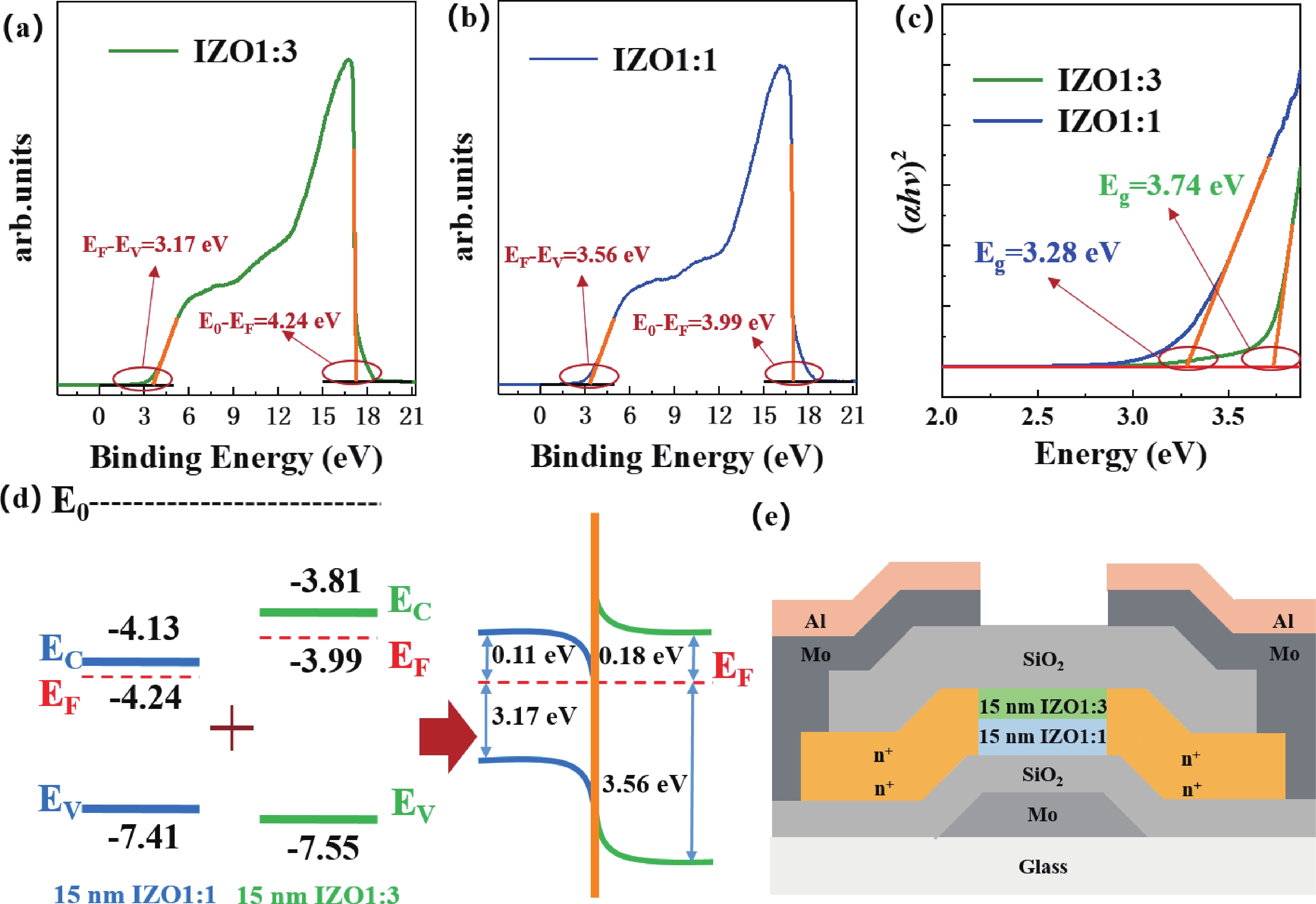
In this work, the bilayer channel was implemented using the amorphous InZnO layers with cation atomic ratios of In : Zn = 1 : 1 at.% and 1 : 3 at.%, respectively named IZO1:1 and IZO1:3. The formation of quantum well at the OS heterojunction interface is closely related to the conduction band (EC) offset between OS layers[1720]. Hence, we firstly investigated the basic energy band structures of IZO1:1 and IZO1:3 layers. The Fermi level (EF), along with the values of EFEV, were measured by the ultraviolet photoelectron spectroscopy (UPS), as shown in Figs. 1(a) and 1(b). The EF of IZO1:1 and IZO1:3 are −3.99 and −4.24 eV, and the EFEV of the two layers are 3.56 and 3.17 eV, respectively. The band gaps (Eg) of IZO1:1 and IZO1:3 were extracted to be 3.28 and 3.74 eV respectively, as shown in Fig. 1(c). Based on the above results, the energy band structures of IZO1:1 and IZO1:3 can be depicted, as illustrated in Fig. 1(d). The EC of IZO1:3 is 0.32 eV higher than that of IZO1:1, suggesting the EC of IZO increases with the increase of Zn content, which is consistent with the previous study on ZnGaO system[21]. Consequently, the large EC offset between IZO1:1 and IZO1:3 is expected to form a quantum well at the heterojunction interface, as plotted in Fig. 1(d).

Fig. 1.  (Color online) The ultraviolet photoelectron spectroscopy of (a) IZO1:3 and (b) IZO1:1 films. (c) Tauc plots for extracting the values of energy gap. (d) Band diagrams and energy level offset of IZO1:1 and IZO1:3. (e) Schematic cross-section of the heterojunction EMMO TFT.

As shown in Fig. 1(e), TFTs with heterojunction channel of IZO1:1 and IZO1:3 were fabricated with the EMMO structure. First, a 100 nm thick molybdenum gate layer was prepared on the glass substrate by sputtering, and it was patterned by lithography. Then, a 100-nm-thick layer of SiO2 was deposited as a gate insulator (GI) by the plasma-enhanced chemical vapor deposition (PECVD). Afterward, the heterojunction channels constituted of 15-nm-thick InZnO1:1 and 15-nm-thick InZnO1:3 were successively prepared in the mixed atmosphere of 29 sccm argon (Ar) and 5 sccm oxygen (O2) by using ceramic targets with chemical compositions respectively of In2O3 : ZnO = 1 : 2 mol% and In2O3 : ZnO = 1 : 6 mol% at room temperature. Next, the heterojunction channel was annealed at 350 °C for 1 h in an O2 atmosphere, and then patterned by the wet etchant. After the bilayer channel is further oxidized using the nitrous oxide (N2O) plasma, a 200-nm-thick layer of PECVD SiO2 was deposited as a passivation layer. Then, contact holes for the bottom gate and source/drain (S/D) were opened using reactive ion etching (RIE). Next, a 100-nm Mo/50-nm Al bilayer was sputtered and patterned to form electrodes. During the final anneal at 400 °C for 2 h in O2 atmosphere, the donor defect-populated n+-S/D was formed in the OS regions sealed the gas-permeable metallic electrodes. Simultaneously, the channel defects, such as VO and Mi, were thermally annihilated by these O2 species diffusing through the permeable SiO2 passivation layer in to OS channel region[15, 16]. The furthest annihilation of oxygen-related channel defects minimizes the possible contributions of native defects to electron mobility[9]. For comparison, single-layer channel TFTs with IZO1:1 and IZO1:3 were fabricated using the aforementioned process flow, and channel thickness is maintained to be 30-nm thick.

The electrical characteristics of TFTs and CV curve were measured by a semiconductor parameter analyzer (Agilent B1500). The characteristics of IZO1:1 and IZO1:3 films (15 nm, annealed at 400 °C for 2 h) were determined by UPS (Thermo K-ALPHA+) and ultraviolet−visible spectrophotometer (Shimadzu UV-2700)

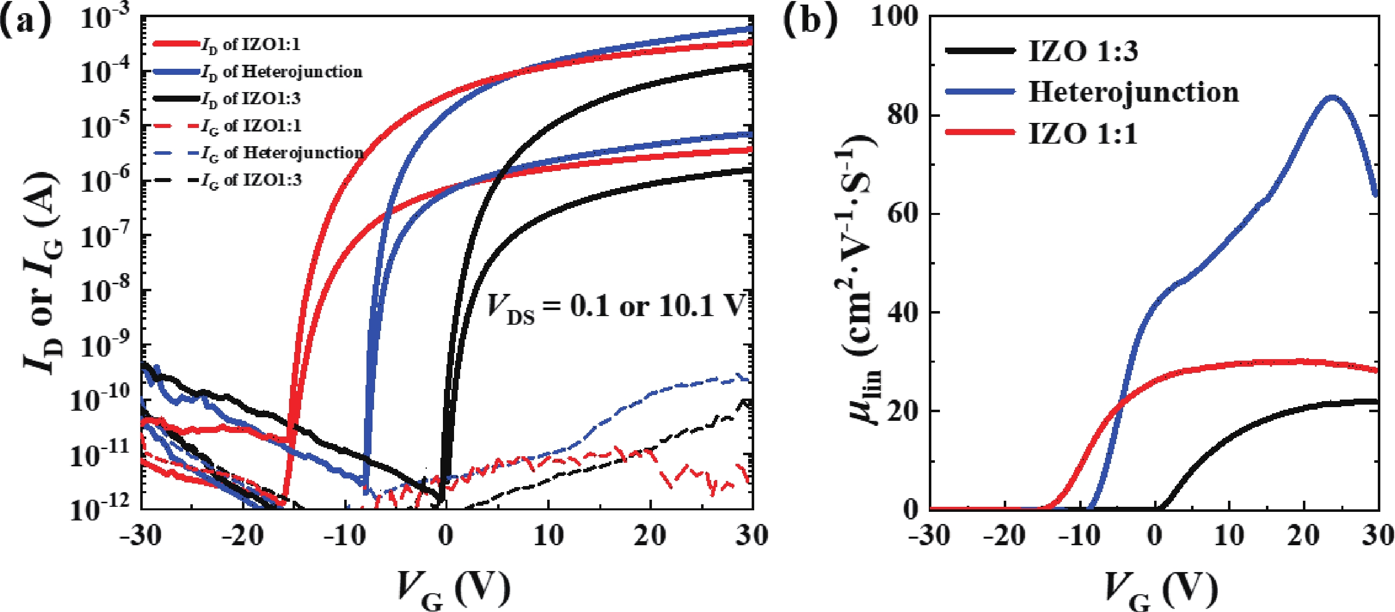
The transfer curves of the IZO1:1, IZO1:3, and IZO1:1/IZO1:3 heterojunction TFT with channel length (L) and width (W) of 100 and 100 µm are shown in Fig. 2(a). Since the threshold voltage (Vth) highly depends on the channel carrier concentration, a more negative Vth of OS TFT often reflects a larger population of channel donor defects[22, 23]. Moreover, the percolation conduction mechanism in OS TFTs further correlates the higher channel carrier concentration with the higher mobility[24]. Herein, the Vth is defined by the gate voltage at L/W-normalized ID = 10−9 A at VDS of 0.1 V and extracted to be −13.5, 1.5, and −6.5 V, respectively for IZO1:1, IZO1:3, and IZO1:1/IZO1:3 TFTs. As expected, a larger In:Zn ratio gives rise to higher channel defect and carrier concentrations[25, 26]. The moderate Vth of heterojunction TFT is thus consistent with the medium cation ratio of the bilayer channel. In contrast, the on-sate current and thus mobility of the bilayer TFT are noticeably higher than those of single-layer TFTs, hinting at an additional conduction mechanism in the bilayer channel.

Fig. 2.  (Color online) (a) The transfer characteristics and (b) linear field-effect mobility versus VG plot of IZO1:1, IZO1:3, and heterojunction TFT.

The linear field-effect mobility (μlin) is given as:

μlin=LWCoxVDS(IDVG).
(1)

Here Cox is the areal capacitance of GI, and the drain-to-source voltage (VDS) is 0.1 V. As shown in Fig. 2(b), the single layer IZO1:1 and IZO1:3 TFT exhibited a μlin of 31.5 and 22.1 cm2·V−1·s−1, respectively. Impressively, the μlin of IZO1:1/IZO1:3 heterojunction TFT is up to 84.3 cm2·V−1·s−1, which is about four times higher than the mobility of IZO1:3 TFT and nearly triple that of IZO1:1 TFT. Considering the moderate defect and carrier concentrations in bilayer channel, a quantum well is most plausibly formed to supply a 2DEG path of higher mobility[10, 17, 27, 28].

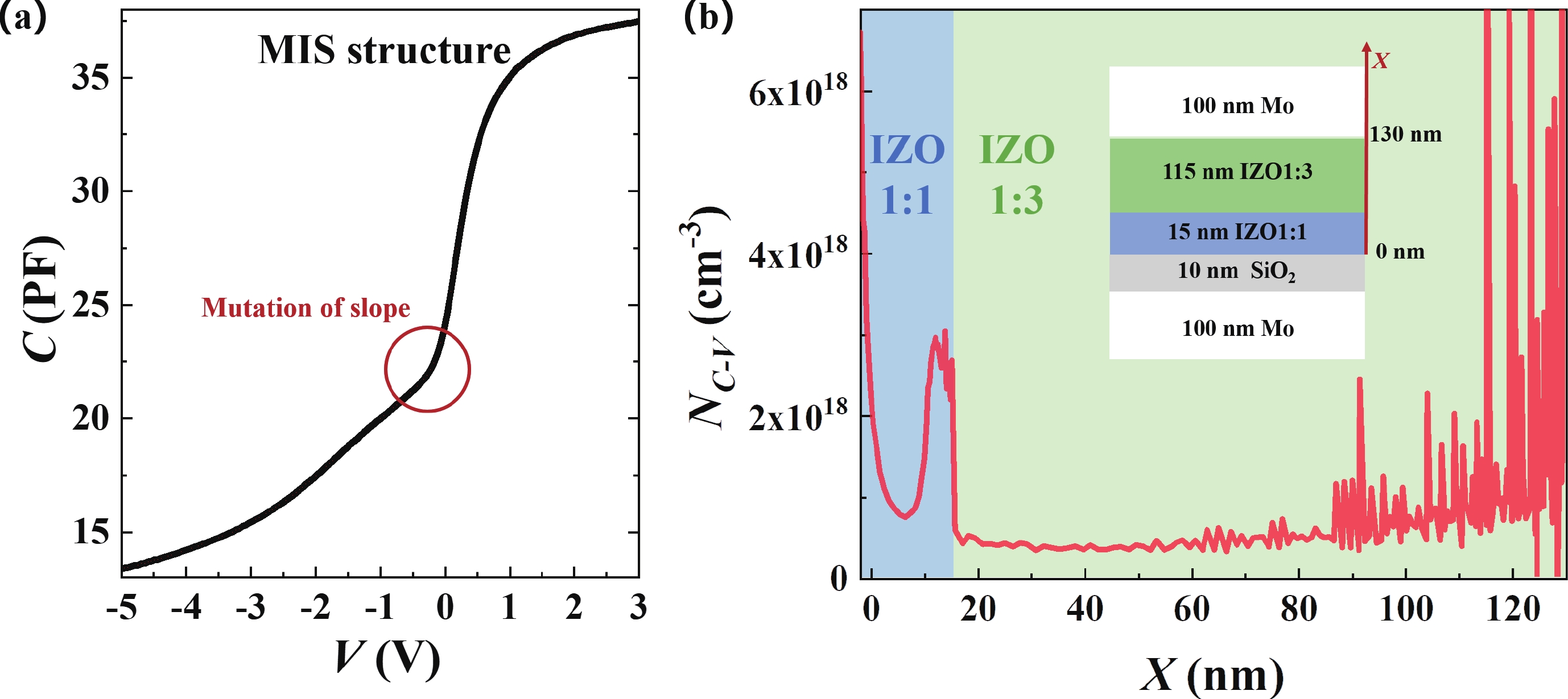
To verify this supposition, we fabricated a metal−insulator−semiconductor (MIS) device to directly evaluate the carrier distribution across the IZO1:1/IZO1:3 heterojunction. Compared with bilayer channel, the thickness of IZO1:1 layer is maintained to be 15 nm, while the thickness of IZO1:3 is increased to 115 nm to avoid the undesired electron injection. The electron concentration (NCV) depth profile is extracted from CV curve by the following equations[29]:

X(V)=Aεε0(1C1Cox).
(2)
NCV=2qεε0A2(C2)V.
(3)

Here, X is the heterojunction depth, C is the measured capacitance as a function of voltage, ε is the permittivity of semiconductor, ε0 is the dielectric constant of vacuum, A is the active area and q is the electron charge. As shown in Fig. 3(a), the CV curve of the heterojunction MIS device exhibits a noticeable mutation of slope. As further analyzed in the NCVX curve (Fig. 3(b)), a surge of NCV is observed near the IZO1:1/IZO1:3 interface, corresponding to the 2DEG. More specifically, the 2DEG quantum well is found to be located at the IZO1:1 side, consistent with the calculated band diagram in Fig. 1(d). Therefore, the high-mobility 2DEG conduction path is attributed to the heterojunction interface formed by the modulation of zinc content.

Fig. 3.  (Color online) (a) CV curve of MIS structure and (b) electron concentration (NC−V) as a function of the heterojunction depth (X).

Besides the significantly boosted mobility, the heterojunction TFT exhibits a more complicated VG dependence of μlin, distinct from the gradually saturated μlin along with the VG increasing in IZO1:1 and IZO1:3 TFTs. This points out that the gate field does not only induct channel electrons, but also influences the 2DEG transport at the heterojunction interface. As shown in Fig. 2(b), the μlin gradually rises up with the VG increasing in the relatively low-VG (LV) realm, while the μlin finally encounters an abrupt drop in the high-VG (HV) range. A similar transition has been observed in heterojunction OS TFTs[9, 17, 30]. A high enough gate field in the opposite direction to the built-in electric field of heterojunction would weaken the quantum well and thus gradually shift the carrier transport from the 2DEG path to the conventional channel/GI interface[30]. This emphasizes the importance of band diagram engineering in the heterojunction OS TFTs.

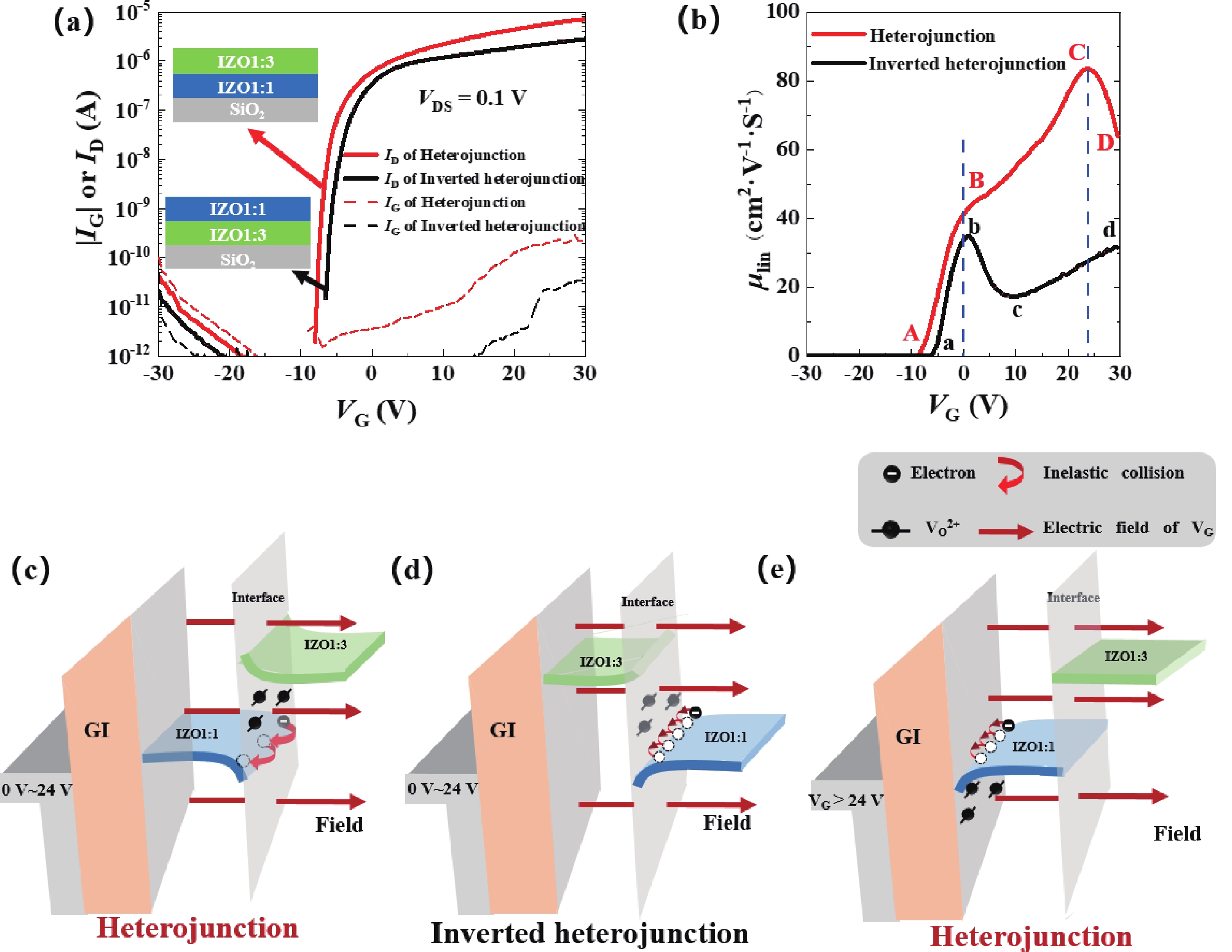
To further investigate the influence of heterojunction band diagram, IZO1:1 and IZO1:3 were reversely stacked to form the IZO1:3/IZO1:1 heterojunction (inverted heterojunction) TFT. As compared in Fig. 4(a), the transfer curves of heterojunction and inverted heterojunction TFTs unsurprisingly have the roughly similar Vth, since both channels have similar populations of channel defects and carriers. Drastic differences are observed in the μlinVG curves in Fig. 4(b). In the AB and ab segments (subthreshold regions), the mobility similarly increases with the increasing VG, since the subthreshold thermal emission current is determined by the VG-modulated source barrier[31].

Fig. 4.  (Color online) (a) The transfer characteristics and (b) linear field-effect mobility versus VG plot of the heterojunction and inverted heterojunction TFT. Energy band diagrams with 3-dimensional views in the (c) heterojunction channel and (d) inverted heterojunction channel operated at LV. (e) Energy band diagrams with 3-dimensional views in the heterojunction channel operated at HV (over 24 V).

As shown in Fig. 4(b), heterojunction and inverted heterojunction TFTs exhibit completely different dependences of μlin on VG. As illustrated in Figs. 4(c) and 4(d), for BC segment of heterojunction TFT, the LV gate field is in the opposite direction to the build-in electric potential and tends to attract the electrons away from the heterojunction interface, while the 2DEG is still confined in the heterojunction quantum well. This results in weakened collisions between electrons and interface defects[32], such as the strongly ionized oxygen vacancy (VO2+) due to extreme band bending[33]. In contrast, the inelastic collision of 2DEG with interface defects in the inverted heterojunction TFT is synergistically enhanced by the built-in electric field and LV gate field, causing a noticeably degraded mobility in the bc segment in Fig. 4(b).

When the gate electric field increases finally to surpass the built-in electric potential in the heterojunction TFT, the 2DEG is gradually pulled out from the suppressed quantum well to the conventional GI/IZO1:1 interface, as illustrated in Fig. 4(e). This results in the abrupt mobility drop in the CD segments in Fig. 4(b). However, the band offset between IZO1:3 and IZO1:1 layers is large enough to form a high built-in potential at the heterojunction and thus ensures a relatively large operation voltage window of 2DEG-enhanced conduction[30]. As for the cd segment, the percolation conduction dominates the electron transport, which is responsible for the increase of mobility to about the same as the mobility of single-layer IZO1:1 channel (about 30 cm2·V−1·s−1).

We have successfully fabricated the high-performance heterojunction InZnO TFTs in the EMMO architecture of inherently low channel defects. The cation ratio-modulated bilayer channel can effectively form high-concentration 2DEG in the interface quantum well. The mobility-boosting capability of 2DEG was found to highly depend on the alignment between the external gate field and the quantum well built-in field, originating from the field-dependent interface collision of 2DEG. Moreover, the VG operation window of such mobility enhancement derives from the competition between these two fields. This work emphasizes the underlying relation between heterojunction band diagram and layer stacking sequence in bilayer OS TFTs. Specifically, we propose that the OS layer with a lower Fermi level can be adjacent to gate insulator to furthest explore the mobility-boosting potential of OS heterojunction channel.

This work was implemented in the Guangdong Technology Center for Oxide Semiconductor Devices and ICs, Guangdong Provincial Key Laboratory of In-Memory Computing Chips, and Shenzhen POC Center of Flexible Electronics.

This work was supported by National Key Research and Development Program (2021YFB3600802),Shenzhen Municipal Scientific Program (JSGG20220831103803007, SGDX20211123145404006),Guangdong Basic and Applied Basic Research Foundation (2022A1515110029).


[1]
Nomura K, Ohta H, Takagi A, et al. Room-temperature fabrication of transparent flexible thin-film transistors using amorphous oxide semiconductors. Nature, 2004, 432(7016), 488 doi: 10.1038/nature03090
[2]
Wu W J, Chen J W, Wang J S, et al. High-resolution flexible AMOLED display integrating gate driver by metal–oxide TFTs. IEEE Electron Device Lett, 2018, 39(11), 1660 doi: 10.1109/LED.2018.2871045
[3]
Lin Y Z, Liu C, Zhang J H, et al. Active-matrix micro-LED display driven by metal oxide TFTs using digital PWM method. IEEE Trans Electron Devices, 2021, 68(11), 5656 doi: 10.1109/TED.2021.3112947
[4]
Furuta M, Koretomo D, Magari Y, et al. Heterojunction channel engineering to enhance performance and reliability of amorphous In-Ga-Zn-O thin-film transistors. Jpn J Appl Phys, 2019, 58(9), 090604 doi: 10.7567/1347-4065/ab1f9f
[5]
Park J C, Lee H N. Improvement of the performance and stability of oxide semiconductor thin-film transistors using double-stacked active layers. IEEE Electron Device Lett, 2012, 33(6), 818 doi: 10.1109/LED.2012.2190036
[6]
Yu X, Zhou N, Smith J, et al. Synergistic approach to high-performance oxide thin film transistors using a bilayer channel architecture. ACS Appl Mater Interfaces, 2013, 5(16), 7983 doi: 10.1021/am402065k
[7]
Chen Z, Han D, Zhao N, et al. High-performance dual-layer channel ITO/TZO TFTs fabricated on glass substrate. Electron Lett, 2014, 50(8), 633 doi: 10.1049/el.2014.0344
[8]
Billah M M, Siddik A B, Kim J B, et al. High-performance coplanar dual-channel a-InGaZnO/a-InZnO semiconductor thin-film transistors with high field-effect mobility. Adv Electron Mater, 2021, 7(3) , 2000896 doi: 10.1002/aelm.202000896
[9]
He J, Li G, Lv Y, et al. Defect self-compensation for high-mobility bilayer InGaZnO/In2O3 thin-film transistor. Adv Electron Mater, 2019, 5(6), 1900125 doi: 10.1002/aelm.201900125
[10]
Faber H, Das S, Lin Y H, et al. Heterojunction oxide thin-film transistors with unprecedented electron mobility grown from solution. Science Adv, 2017, 3(3), 1602640 doi: 10.1126/sciadv.1602640
[11]
Wang P F, Yang H, Li J Y, et al. Synergistically enhanced performance and reliability of abrupt metal-oxide heterojunction transistor. Adv Electron Mater, 2023, 9(1), 2200807 doi: 10.1002/aelm.202200807
[12]
Lan L, Zhao M, Xiong N. Low-voltage high-stability indium-zinc oxide thin-film transistor gated by anodized neodymium-doped aluminum. IEEE Electron Device Lett, 2012, 33(6), 827 doi: 10.1109/LED.2012.2190966
[13]
David C P, Burag Y, Zach B, et al. Amorphous IZO-based transparent thin film transistors. Thin Solid Films, 2008, 516(17), 5894 doi: 10.1016/j.tsf.2007.10.081
[14]
Yue S, Lu J, Lu R, et al. Ultrathin-film transistors based on ultrathin amorphous InZnO films. IEEE Trans Electron Devices, 2019, 66(7), 2960 doi: 10.1109/TED.2019.2913866
[15]
Lu L, Li J, Kwok H S, et al. High-performance and reliable elevated-metal metal-oxide thin-film transistor for high-resolution displays. IEEE Electron Devices Meeting, 2016, 7838526 doi: 10.1109/IEDM.2016.7838526
[16]
Lu L, Wong M. The resistivity of zinc oxide under different annealing configurations and its impact on the leakage characteristics of zinc oxide thin-film transistors. IEEE Trans Electron Devices, 2014, 61(4), 1077 doi: 10.1109/TED.2014.2302431
[17]
Koretomo D, Hamada S, Magari Y, et al. Quantum confinement effect in amorphous In-Ga-Zn-O heterojunction channels for thin-film transistors. Mater, 2020, 13(8), 1935 doi: 10.3390/ma13081935
[18]
Tsukazaki A, Ohtomo A, Kawasaki M. Surface and interface engineering of ZnO based heterostructures fabricated by pulsed-laser deposition. J Phys D Appl Phys, 2014, 47(3), 331 doi: 10.1088/0022-3727/47/3/034003
[19]
Tampo H, Shibata H, Matsubara K, et al. Two-dimensional electron gas in Zn polar ZnMgO/ZnO heterostructures grown by radical source molecular beam epitaxy. Appl Phys Lett, 2006, 89(13), 112106 doi: 10.1063/1.2357588
[20]
Guo M, Ou H, Xie D Y, et al. Critical assessment of the high carrier mobility of bilayer In2O3/IGZO transistors and the underlying mechanisms. Adv Electron Mater, 2023, 9(3), 2201184 doi: 10.1002/aelm.202201184
[21]
Kim J, Bang J, Nakamura N, et al. Ultra-wide bandgap amorphous oxide semiconductors for NBIS-free thin-film transistors. APL Mater, 2019, 7(2), 022501 doi: 10.1063/1.5053762
[22]
Janotti A, Walle C G V D. Native point defects in ZnO. Phys Rev B, 2007, 76(16), 165202. doi: 10.1103/PhysRevB.76.165202
[23]
Leenheer A J, Perkins J D, Van H, et al. General mobility and carrier concentration relationship in transparent amorphous indium zinc oxide films. Phys Rev B, 2008, 77(11), 115215 doi: 10.1103/PhysRevB.77.115215
[24]
Lee S, Ghaffarzadeh K, Nathan A, et al. Trap-limited and percolation conduction mechanisms in amorphous oxide semiconductor thin film transistors. Appl Phys Lett, 2011, 98(20), 203508 doi: 10.1063/1.3589371
[25]
Koo C Y, Song K, Jun T, et al. Low temperature solution-processed InZnO thin-film transistors. J Electrochem Soc, 2010, 157(4), 111 doi: 10.1149/1.3298886
[26]
Liang Y K, Zheng J Y, Lin J W, et al. Effects of In/Zn composition on the performance of ultra-thin atomic layer deposited InxZn1-xO channel thin-film transistors. 2023 7th IEEE Electron Devices Technology & Manufacturing Conference, 2023, 1 doi: 10.1109/EDTM55494.2023.10103052
[27]
Cho M H, Choi C H, Kim M J, et al. High-performance indium-based oxide transistors with multiple channels through nanolaminate structure fabricated by plasma-enhanced atomic layer deposition. ACS Appl Mater Interfaces, 2023, 15(15), 19137 doi: 10.1021/acsami.3c00038
[28]
Khim D, Lin Y H, Nam, S, et al. Modulation-doped In2O3/ZnO heterojunction transistors processed from solution. Adv Mater, 2017, 29(19), 1605837 doi: 10.1002/adma.201605837
[29]
Lin Y H, Faber H, Labram J G, et al. High electron mobility thin-film transistors based on solution-processed semiconducting metal oxide heterojunctions and quasi-superlattices. Adv Sci, 2015, 2(7), 1500058 doi: 10.1002/advs.201500058
[30]
Yang H, Zhou X L, Lu L, et al. Investigation to the carrier transport properties in heterojunction-channel amorphous oxides thin-film transistors using dual-gate bias. IEEE Electron Device Lett, 2023, 44(1), 68 doi: 10.1109/LED.2022.3223080
[31]
Liu C, Li G T, Di P R, et al. Device physics of contact issues for the overestimation and underestimation of carrier mobility in field-effect transistors. Phys Rev Appl, 2017, 8(3), 034020 doi: 10.1103/PhysRevApplied.8.034020
[32]
Vecchi M C, Greiner A, Rudan M. Modeling surface scattering effects in the solution of the BTE based on spherical harmonics expansion. ESSDERC '96, Proceedings of the 26th European Solid State Device Research Conference, 1996, 825
[33]
Zhu G, Zhang M, Member S, et al. Significant degradation reduction in metal oxide thin-film transistors via the interaction of ionized oxygen vacancy redistribution, self-heating effect, and hot carrier effect. IEEE Transactions on Electron Devices, 2023, 70(8), 4198 doi: 10.1109/TED.2023.3283940
Fig. 1.  (Color online) The ultraviolet photoelectron spectroscopy of (a) IZO1:3 and (b) IZO1:1 films. (c) Tauc plots for extracting the values of energy gap. (d) Band diagrams and energy level offset of IZO1:1 and IZO1:3. (e) Schematic cross-section of the heterojunction EMMO TFT.

Fig. 2.  (Color online) (a) The transfer characteristics and (b) linear field-effect mobility versus VG plot of IZO1:1, IZO1:3, and heterojunction TFT.

Fig. 3.  (Color online) (a) CV curve of MIS structure and (b) electron concentration (NC−V) as a function of the heterojunction depth (X).

Fig. 4.  (Color online) (a) The transfer characteristics and (b) linear field-effect mobility versus VG plot of the heterojunction and inverted heterojunction TFT. Energy band diagrams with 3-dimensional views in the (c) heterojunction channel and (d) inverted heterojunction channel operated at LV. (e) Energy band diagrams with 3-dimensional views in the heterojunction channel operated at HV (over 24 V).

[1]
Nomura K, Ohta H, Takagi A, et al. Room-temperature fabrication of transparent flexible thin-film transistors using amorphous oxide semiconductors. Nature, 2004, 432(7016), 488 doi: 10.1038/nature03090
[2]
Wu W J, Chen J W, Wang J S, et al. High-resolution flexible AMOLED display integrating gate driver by metal–oxide TFTs. IEEE Electron Device Lett, 2018, 39(11), 1660 doi: 10.1109/LED.2018.2871045
[3]
Lin Y Z, Liu C, Zhang J H, et al. Active-matrix micro-LED display driven by metal oxide TFTs using digital PWM method. IEEE Trans Electron Devices, 2021, 68(11), 5656 doi: 10.1109/TED.2021.3112947
[4]
Furuta M, Koretomo D, Magari Y, et al. Heterojunction channel engineering to enhance performance and reliability of amorphous In-Ga-Zn-O thin-film transistors. Jpn J Appl Phys, 2019, 58(9), 090604 doi: 10.7567/1347-4065/ab1f9f
[5]
Park J C, Lee H N. Improvement of the performance and stability of oxide semiconductor thin-film transistors using double-stacked active layers. IEEE Electron Device Lett, 2012, 33(6), 818 doi: 10.1109/LED.2012.2190036
[6]
Yu X, Zhou N, Smith J, et al. Synergistic approach to high-performance oxide thin film transistors using a bilayer channel architecture. ACS Appl Mater Interfaces, 2013, 5(16), 7983 doi: 10.1021/am402065k
[7]
Chen Z, Han D, Zhao N, et al. High-performance dual-layer channel ITO/TZO TFTs fabricated on glass substrate. Electron Lett, 2014, 50(8), 633 doi: 10.1049/el.2014.0344
[8]
Billah M M, Siddik A B, Kim J B, et al. High-performance coplanar dual-channel a-InGaZnO/a-InZnO semiconductor thin-film transistors with high field-effect mobility. Adv Electron Mater, 2021, 7(3) , 2000896 doi: 10.1002/aelm.202000896
[9]
He J, Li G, Lv Y, et al. Defect self-compensation for high-mobility bilayer InGaZnO/In2O3 thin-film transistor. Adv Electron Mater, 2019, 5(6), 1900125 doi: 10.1002/aelm.201900125
[10]
Faber H, Das S, Lin Y H, et al. Heterojunction oxide thin-film transistors with unprecedented electron mobility grown from solution. Science Adv, 2017, 3(3), 1602640 doi: 10.1126/sciadv.1602640
[11]
Wang P F, Yang H, Li J Y, et al. Synergistically enhanced performance and reliability of abrupt metal-oxide heterojunction transistor. Adv Electron Mater, 2023, 9(1), 2200807 doi: 10.1002/aelm.202200807
[12]
Lan L, Zhao M, Xiong N. Low-voltage high-stability indium-zinc oxide thin-film transistor gated by anodized neodymium-doped aluminum. IEEE Electron Device Lett, 2012, 33(6), 827 doi: 10.1109/LED.2012.2190966
[13]
David C P, Burag Y, Zach B, et al. Amorphous IZO-based transparent thin film transistors. Thin Solid Films, 2008, 516(17), 5894 doi: 10.1016/j.tsf.2007.10.081
[14]
Yue S, Lu J, Lu R, et al. Ultrathin-film transistors based on ultrathin amorphous InZnO films. IEEE Trans Electron Devices, 2019, 66(7), 2960 doi: 10.1109/TED.2019.2913866
[15]
Lu L, Li J, Kwok H S, et al. High-performance and reliable elevated-metal metal-oxide thin-film transistor for high-resolution displays. IEEE Electron Devices Meeting, 2016, 7838526 doi: 10.1109/IEDM.2016.7838526
[16]
Lu L, Wong M. The resistivity of zinc oxide under different annealing configurations and its impact on the leakage characteristics of zinc oxide thin-film transistors. IEEE Trans Electron Devices, 2014, 61(4), 1077 doi: 10.1109/TED.2014.2302431
[17]
Koretomo D, Hamada S, Magari Y, et al. Quantum confinement effect in amorphous In-Ga-Zn-O heterojunction channels for thin-film transistors. Mater, 2020, 13(8), 1935 doi: 10.3390/ma13081935
[18]
Tsukazaki A, Ohtomo A, Kawasaki M. Surface and interface engineering of ZnO based heterostructures fabricated by pulsed-laser deposition. J Phys D Appl Phys, 2014, 47(3), 331 doi: 10.1088/0022-3727/47/3/034003
[19]
Tampo H, Shibata H, Matsubara K, et al. Two-dimensional electron gas in Zn polar ZnMgO/ZnO heterostructures grown by radical source molecular beam epitaxy. Appl Phys Lett, 2006, 89(13), 112106 doi: 10.1063/1.2357588
[20]
Guo M, Ou H, Xie D Y, et al. Critical assessment of the high carrier mobility of bilayer In2O3/IGZO transistors and the underlying mechanisms. Adv Electron Mater, 2023, 9(3), 2201184 doi: 10.1002/aelm.202201184
[21]
Kim J, Bang J, Nakamura N, et al. Ultra-wide bandgap amorphous oxide semiconductors for NBIS-free thin-film transistors. APL Mater, 2019, 7(2), 022501 doi: 10.1063/1.5053762
[22]
Janotti A, Walle C G V D. Native point defects in ZnO. Phys Rev B, 2007, 76(16), 165202. doi: 10.1103/PhysRevB.76.165202
[23]
Leenheer A J, Perkins J D, Van H, et al. General mobility and carrier concentration relationship in transparent amorphous indium zinc oxide films. Phys Rev B, 2008, 77(11), 115215 doi: 10.1103/PhysRevB.77.115215
[24]
Lee S, Ghaffarzadeh K, Nathan A, et al. Trap-limited and percolation conduction mechanisms in amorphous oxide semiconductor thin film transistors. Appl Phys Lett, 2011, 98(20), 203508 doi: 10.1063/1.3589371
[25]
Koo C Y, Song K, Jun T, et al. Low temperature solution-processed InZnO thin-film transistors. J Electrochem Soc, 2010, 157(4), 111 doi: 10.1149/1.3298886
[26]
Liang Y K, Zheng J Y, Lin J W, et al. Effects of In/Zn composition on the performance of ultra-thin atomic layer deposited InxZn1-xO channel thin-film transistors. 2023 7th IEEE Electron Devices Technology & Manufacturing Conference, 2023, 1 doi: 10.1109/EDTM55494.2023.10103052
[27]
Cho M H, Choi C H, Kim M J, et al. High-performance indium-based oxide transistors with multiple channels through nanolaminate structure fabricated by plasma-enhanced atomic layer deposition. ACS Appl Mater Interfaces, 2023, 15(15), 19137 doi: 10.1021/acsami.3c00038
[28]
Khim D, Lin Y H, Nam, S, et al. Modulation-doped In2O3/ZnO heterojunction transistors processed from solution. Adv Mater, 2017, 29(19), 1605837 doi: 10.1002/adma.201605837
[29]
Lin Y H, Faber H, Labram J G, et al. High electron mobility thin-film transistors based on solution-processed semiconducting metal oxide heterojunctions and quasi-superlattices. Adv Sci, 2015, 2(7), 1500058 doi: 10.1002/advs.201500058
[30]
Yang H, Zhou X L, Lu L, et al. Investigation to the carrier transport properties in heterojunction-channel amorphous oxides thin-film transistors using dual-gate bias. IEEE Electron Device Lett, 2023, 44(1), 68 doi: 10.1109/LED.2022.3223080
[31]
Liu C, Li G T, Di P R, et al. Device physics of contact issues for the overestimation and underestimation of carrier mobility in field-effect transistors. Phys Rev Appl, 2017, 8(3), 034020 doi: 10.1103/PhysRevApplied.8.034020
[32]
Vecchi M C, Greiner A, Rudan M. Modeling surface scattering effects in the solution of the BTE based on spherical harmonics expansion. ESSDERC '96, Proceedings of the 26th European Solid State Device Research Conference, 1996, 825
[33]
Zhu G, Zhang M, Member S, et al. Significant degradation reduction in metal oxide thin-film transistors via the interaction of ionized oxygen vacancy redistribution, self-heating effect, and hot carrier effect. IEEE Transactions on Electron Devices, 2023, 70(8), 4198 doi: 10.1109/TED.2023.3283940
1

Indium–gallium–zinc–oxide thin-film transistors: Materials, devices, and applications

Ying Zhu, Yongli He, Shanshan Jiang, Li Zhu, Chunsheng Chen, et al.

Journal of Semiconductors, 2021, 42(3): 031101. doi: 10.1088/1674-4926/42/3/031101

2

Oxide-based thin film transistors for flexible electronics

Yongli He, Xiangyu Wang, Ya Gao, Yahui Hou, Qing Wan, et al.

Journal of Semiconductors, 2018, 39(1): 011005. doi: 10.1088/1674-4926/39/1/011005

3

Review of recent progresses on flexible oxide semiconductor thin film transistors based on atomic layer deposition processes

Jiazhen Sheng, Ki-Lim Han, TaeHyun Hong, Wan-Ho Choi, Jin-Seong Park, et al.

Journal of Semiconductors, 2018, 39(1): 011008. doi: 10.1088/1674-4926/39/1/011008

4

Large signal and noise properties of heterojunction AlxGa1-xAs/GaAs DDRIMPATTs

Suranjana Banerjee, Monojit Mitra

Journal of Semiconductors, 2016, 37(6): 064002. doi: 10.1088/1674-4926/37/6/064002

5

Detection of lead ions with AlGaAs/InGaAs pseudomorphic high electron mobility transistor

Jiqiang Niu, Yang Zhang, Min Guan, Chengyan Wang, Lijie Cui, et al.

Journal of Semiconductors, 2016, 37(11): 114003. doi: 10.1088/1674-4926/37/11/114003

6

Progress in complementary metal-oxide-semiconductor silicon photonics and optoelectronic integrated circuits

Hongda Chen, Zan Zhang, Beiju Huang, Luhong Mao, Zanyun Zhang, et al.

Journal of Semiconductors, 2015, 36(12): 121001. doi: 10.1088/1674-4926/36/12/121001

7

Effects of interface trap density on the electrical performance of amorphous InSnZnO thin-film transistor

Yongye Liang, Kyungsoo Jang, S. Velumani, Cam Phu Thi Nguyen, Junsin Yi, et al.

Journal of Semiconductors, 2015, 36(2): 024007. doi: 10.1088/1674-4926/36/2/024007

8

Analysis of charge density and Fermi level of AlInSb/InSb single-gate high electron mobility transistor

S. Theodore Chandra, N. B. Balamurugan, M. Bhuvaneswari, N. Anbuselvan, N. Mohankumar, et al.

Journal of Semiconductors, 2015, 36(6): 064003. doi: 10.1088/1674-4926/36/6/064003

9

Compact analytical model for single gate AlInSb/InSb high electron mobility transistors

S. Theodore Chandra, N.B. Balamurugan, G. Subalakshmi, T. Shalini, G. Lakshmi Priya, et al.

Journal of Semiconductors, 2014, 35(11): 114003. doi: 10.1088/1674-4926/35/11/114003

10

Fabrication of SiC nanowire thin-film transistors using dielectrophoresis

Dai Zhenqing, Zhang Liying, Chen Changxin, Qian Bingjian, Xu Dong, et al.

Journal of Semiconductors, 2012, 33(11): 114001. doi: 10.1088/1674-4926/33/11/114001

11

Giant magnetoresistance in a two-dimensional electron gas modulated by ferromagnetic and Schottky metal stripes

Lu Jianduo, Xu Bin

Journal of Semiconductors, 2012, 33(7): 074007. doi: 10.1088/1674-4926/33/7/074007

12

Influence of Ni Schottky contact thickness on two-dimensional electron-gas sheet carrier concentration of strained Al0.3Ga0.7N/GaN heterostructures

Zhao Jianzhi, Lin Zhaojun, Lü Yuanjie, Corrigan Timothy D, Meng Lingguo, et al.

Journal of Semiconductors, 2010, 31(8): 084007. doi: 10.1088/1674-4926/31/8/084007

13

Comparison of electron transmittances and tunneling currents in an anisotropic TiNx/HfO2/SiO2/p-Si(100) metal–oxide–semiconductor (MOS) capacitor calculated using exponential- and Airy-wavefunction app

Fatimah A. Noor, Mikrajuddin Abdullah, Sukirno, Khairurrijal

Journal of Semiconductors, 2010, 31(12): 124002. doi: 10.1088/1674-4926/31/12/124002

14

Phonon-induced magnetoresistance oscillations in a high-mobility quantum well

Zhou Qisheng, Cao Juncheng, Qi Ming, Lei Xiaolin

Journal of Semiconductors, 2010, 31(9): 092001. doi: 10.1088/1674-4926/31/9/092001

15

Optical and electrical properties of N-doped ZnO and fabrication of thin-film transistors

Zhu Xiaming, Wu Huizhen, Wang Shuangjiang, Zhang Yingying, Cai Chunfeng, et al.

Journal of Semiconductors, 2009, 30(3): 033001. doi: 10.1088/1674-4926/30/3/033001

16

Sensitive properties of In-based compound semiconductor oxide to Cl2 gas

Zhao Wenjie, Shi Yunbo, Xiu Debin, Lei Tingping, Feng Qiaohua, et al.

Journal of Semiconductors, 2009, 30(3): 034010. doi: 10.1088/1674-4926/30/3/034010

17

Quantum and Transport Mobilities of a Two-Dimensional Electron Gas in the Presence of the Rashba Spin-Orbit Interaction

Xu Wen

Chinese Journal of Semiconductors , 2006, 27(2): 204-217.

18

Analysis of PTCDA/ITO Surface and Interface Using X-ray Photoelectron Spectroscopy and Atomic Force Microscopy

Tang Ning, Shen Bo, Wang Maojun, Yang Zhijian, Xu Ke, et al.

Chinese Journal of Semiconductors , 2006, 27(2): 235-238.

19

Passively Mode Locked Diode-End-Pumped Yb∶YAB Laser with High Reflectivity Type Semiconductor Saturable Absorption Mirror

Wang Yonggang, Ma Xiaoyu, Xue Yinghong, Sun Hong,Zhang Zhigang,and Wang Qingyue

Chinese Journal of Semiconductors , 2005, 26(2): 250-253.

20

AlGaN/GaN High Electron Mobility Transistors on Sapphires with fmax of 100GHz

Li Xianjie, Zeng Qingming, Zhou Zhou, Liu Yugui, Qiao Shuyun, et al.

Chinese Journal of Semiconductors , 2005, 26(11): 2049-2052.

1. Lim, S.-H., Mah, D.-G., Cho, W.-J. Enhancing oxide semiconductor channel performance through heterojunction engineering of indium-tungsten oxide and indium-gallium-zinc oxide. Japanese Journal of Applied Physics, Part 1: Regular Papers and Short Notes and Review Papers, 2024, 63(12): 12SP03. doi:10.35848/1347-4065/ad94fc
  • Search

    Advanced Search >>

    GET CITATION

    Xiao Li, Zhikang Ma, Jinxiong Li, Wengao Pan, Congwei Liao, Shengdong Zhang, Zhuo Gao, Dong Fu, Lei Lu. Heterojunction-engineered carrier transport in elevated-metal metal-oxide thin-film transistors[J]. Journal of Semiconductors, 2024, 45(10): 102301. doi: 10.1088/1674-4926/24040016
    X Li, Z K Ma, J X Li, W G Pan, C W Liao, S D Zhang, Z Gao, D Fu, and L Lu, Heterojunction-engineered carrier transport in elevated-metal metal-oxide thin-film transistors[J]. J. Semicond., 2024, 45(10), 102301 doi: 10.1088/1674-4926/24040016
    shu

    Export: BibTex EndNote

    Article Metrics

    Article views: 661 Times PDF downloads: 79 Times Cited by: 1 Times

    History

    Received: 11 April 2024 Revised: 03 June 2024 Online: Accepted Manuscript: 19 June 2024Uncorrected proof: 19 June 2024Published: 15 October 2024

    Catalog

      Email This Article

      User name:
      Email:*请输入正确邮箱
      Code:*验证码错误
      Xiao Li, Zhikang Ma, Jinxiong Li, Wengao Pan, Congwei Liao, Shengdong Zhang, Zhuo Gao, Dong Fu, Lei Lu. Heterojunction-engineered carrier transport in elevated-metal metal-oxide thin-film transistors[J]. Journal of Semiconductors, 2024, 45(10): 102301. doi: 10.1088/1674-4926/24040016 ****X Li, Z K Ma, J X Li, W G Pan, C W Liao, S D Zhang, Z Gao, D Fu, and L Lu, Heterojunction-engineered carrier transport in elevated-metal metal-oxide thin-film transistors[J]. J. Semicond., 2024, 45(10), 102301 doi: 10.1088/1674-4926/24040016
      Citation:
      Xiao Li, Zhikang Ma, Jinxiong Li, Wengao Pan, Congwei Liao, Shengdong Zhang, Zhuo Gao, Dong Fu, Lei Lu. Heterojunction-engineered carrier transport in elevated-metal metal-oxide thin-film transistors[J]. Journal of Semiconductors, 2024, 45(10): 102301. doi: 10.1088/1674-4926/24040016 ****
      X Li, Z K Ma, J X Li, W G Pan, C W Liao, S D Zhang, Z Gao, D Fu, and L Lu, Heterojunction-engineered carrier transport in elevated-metal metal-oxide thin-film transistors[J]. J. Semicond., 2024, 45(10), 102301 doi: 10.1088/1674-4926/24040016

      Heterojunction-engineered carrier transport in elevated-metal metal-oxide thin-film transistors

      DOI: 10.1088/1674-4926/24040016
      CSTR: 32376.14.1674-4926.24040016
      More Information
      • Xiao Li received his BS degrees in state key laboratory of chemical engineering from East China University of Science technology, MS degrees in state key laboratory of luminescent materials and devices from South China University of technology. Now, he is a PhD student at Peking University under the supervision of prof. Lei Lu. His research focus on thin-film transistors and flexible display
      • Shengdong Zhang received his BS and MS degrees in Electronic Engineering from Southeast University, and his PhD degree in Microelectronics from Peking University. In 2002, he joined School of Electronics Engineering and Computer Science at Peking University. He is currently a professor in School of Electronic and Computer Engineering at Peking University Shenzhen Graduate School. His research interests include integrated circuit design, thin-film transistors and flexible display
      • Lei Lu received his BS and MS degrees in Microelectronics from Soochow University, and his PhD degree in Electronic and Computer Engineering from the Hong Kong University of Science and Technology, he worked at the Hong Kong University of Science and Technology from 2015 to 2019, and joined School of Electronic and Computer Engineering at Peking University Shenzhen Graduate School in 2019, where he is now an assistant professor. His research interests include semiconductor devices, advanced display technology and flexible electronics
      • Corresponding author: lulei@pku.edu.cn
      • Received Date: 2024-04-11
      • Revised Date: 2024-06-03
      • Available Online: 2024-06-19

      Catalog

        /

        DownLoad:  Full-Size Img  PowerPoint
        Return
        Return