Issue Browser
Volume 46, Issue 9,
Sep 2025
J. Semicond.
2025, 46(9): 091701 doi: 10.1088/1674-4926/25030023

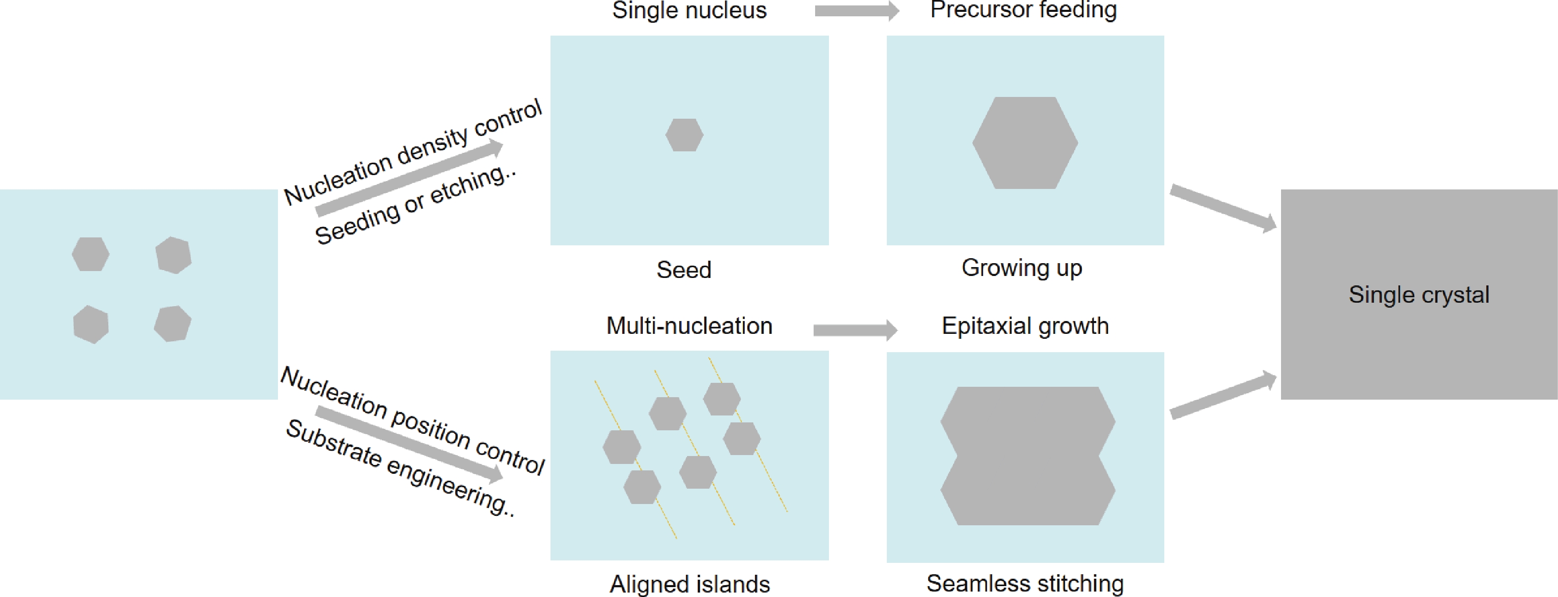
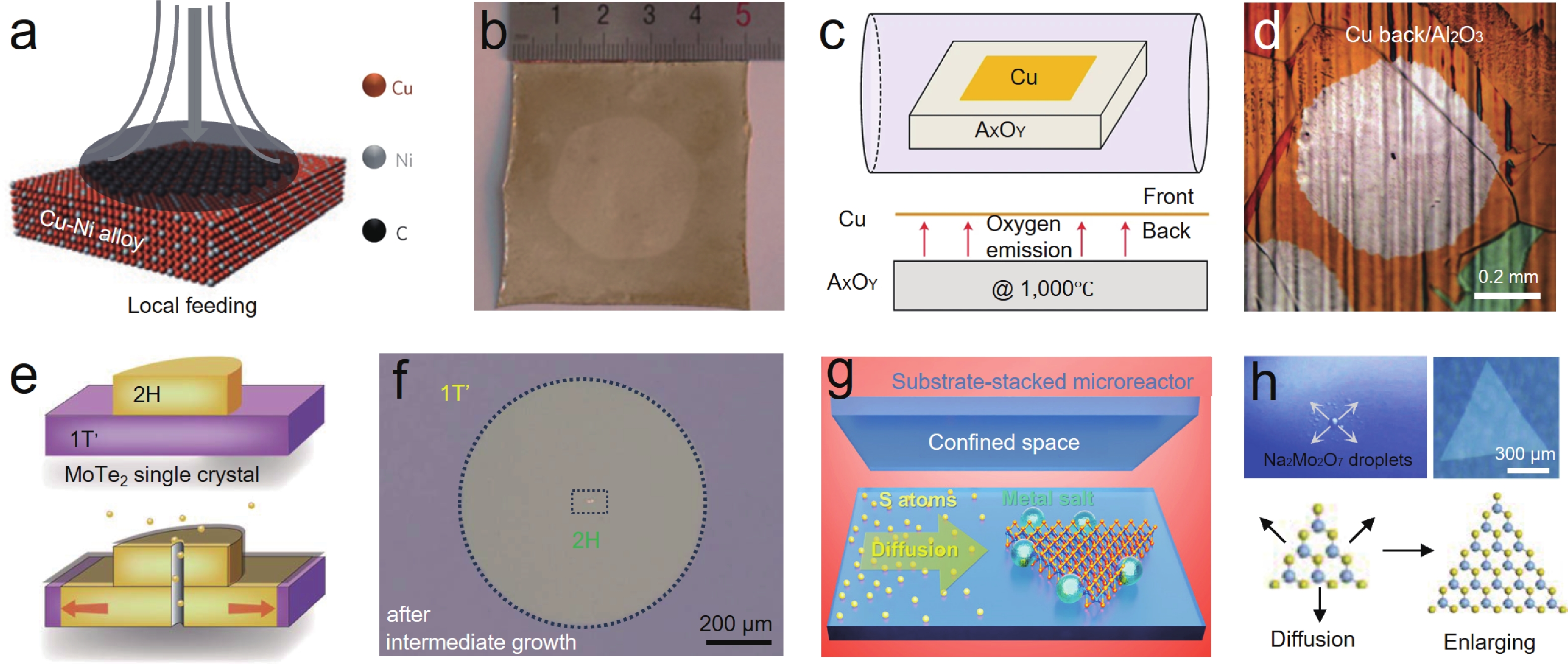
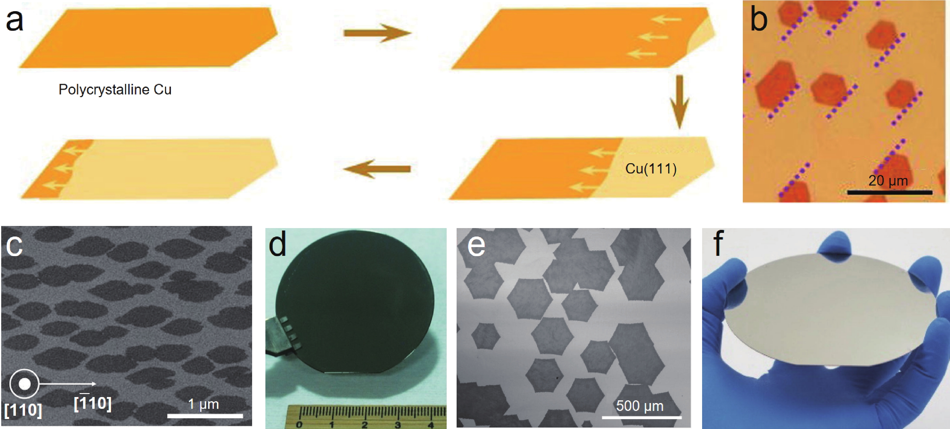
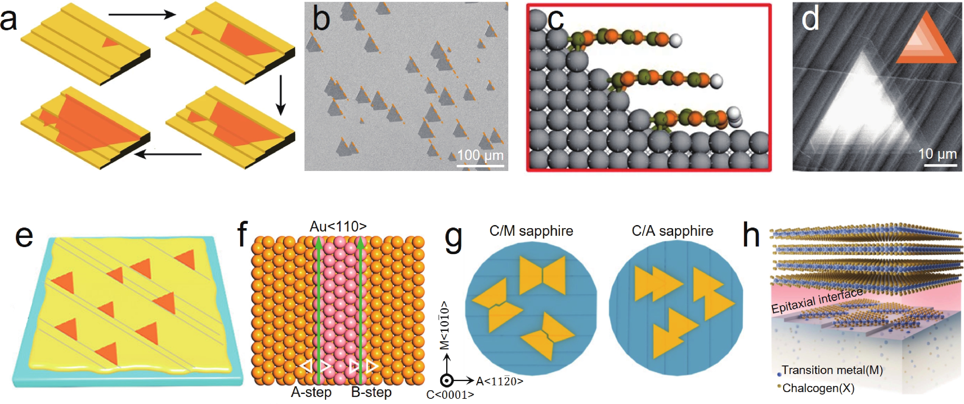
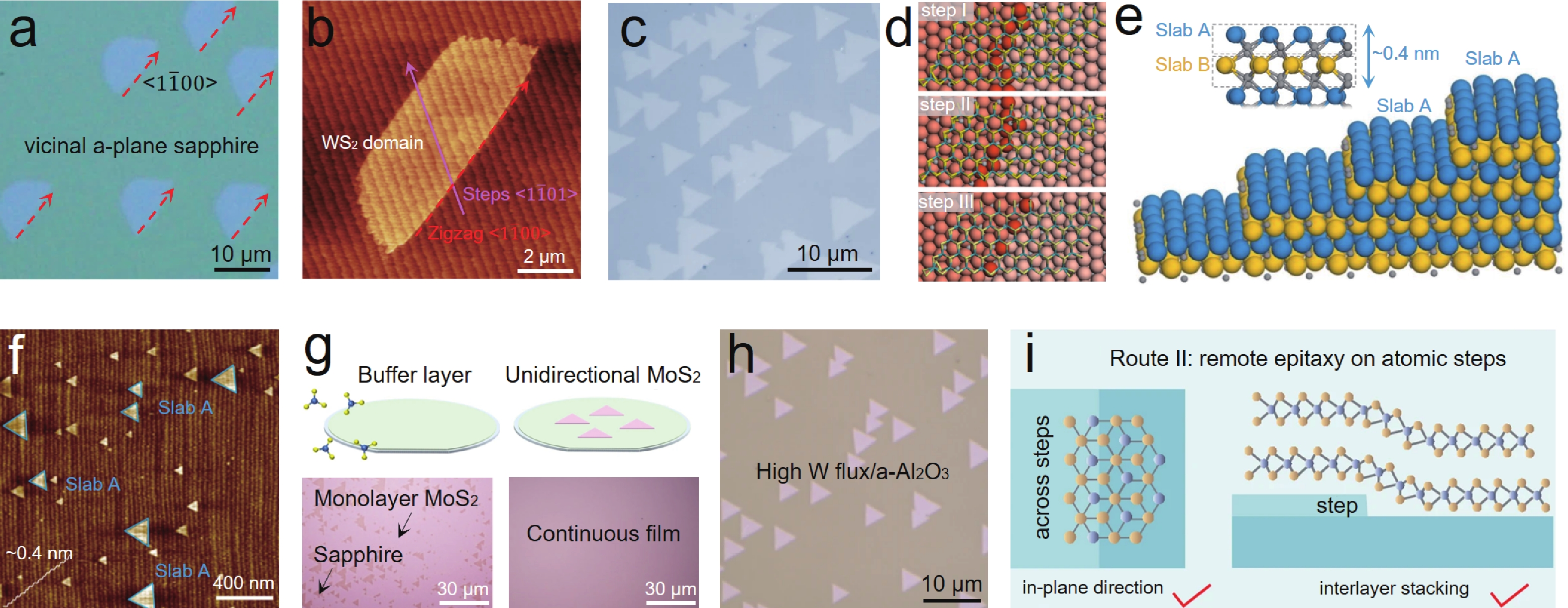
The unique structure and exceptional properties of two-dimensional (2D) materials offer significant potential for transformative advancements in semiconductor industry. Similar to the reliance on wafer-scale single-crystal ingots for silicon-based chips, practical applications of 2D materials at the chip level need large-scale, high-quality production of 2D single crystals. Over the past two decades, the size of 2D single-crystals has been improved to wafer or meter scale, where the nucleation control during the growth process is particularly important. Therefore, it is essential to conduct a comprehensive review of nucleation control to gain fundamental insights into the growth of 2D single-crystal materials. This review mainly focuses on two aspects: controlling nucleation density to enable the growth from a single nucleus, and controlling nucleation position to achieve the unidirectionally aligned islands and subsequent seamless stitching. Finally, we provide an overview and forecast of the strategic pathways for emerging 2D materials.
J. Semicond.
2025, 46(9): 092101 doi: 10.1088/1674-4926/25020006
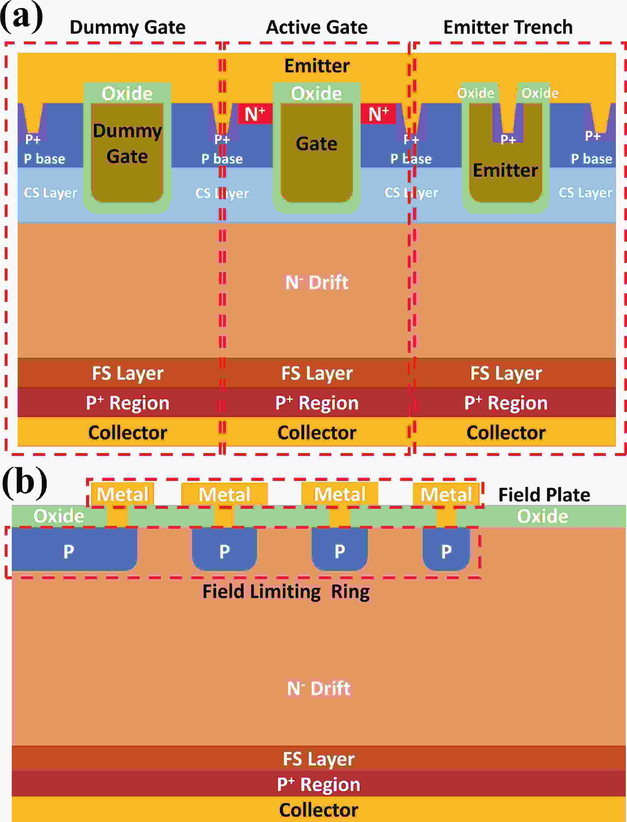
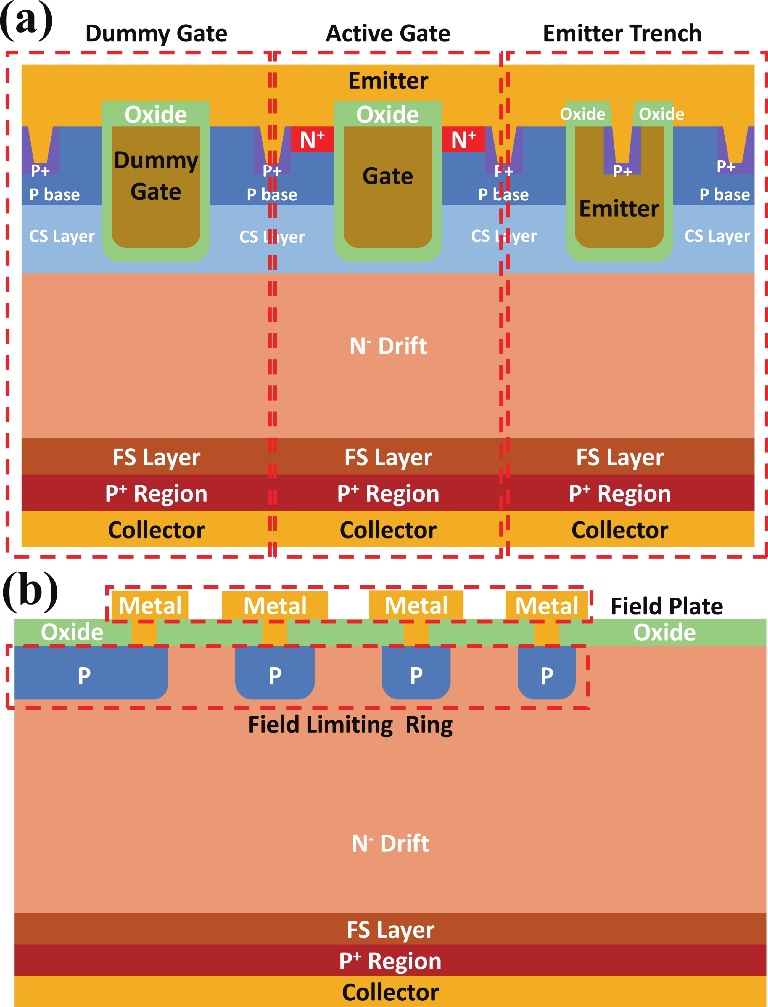
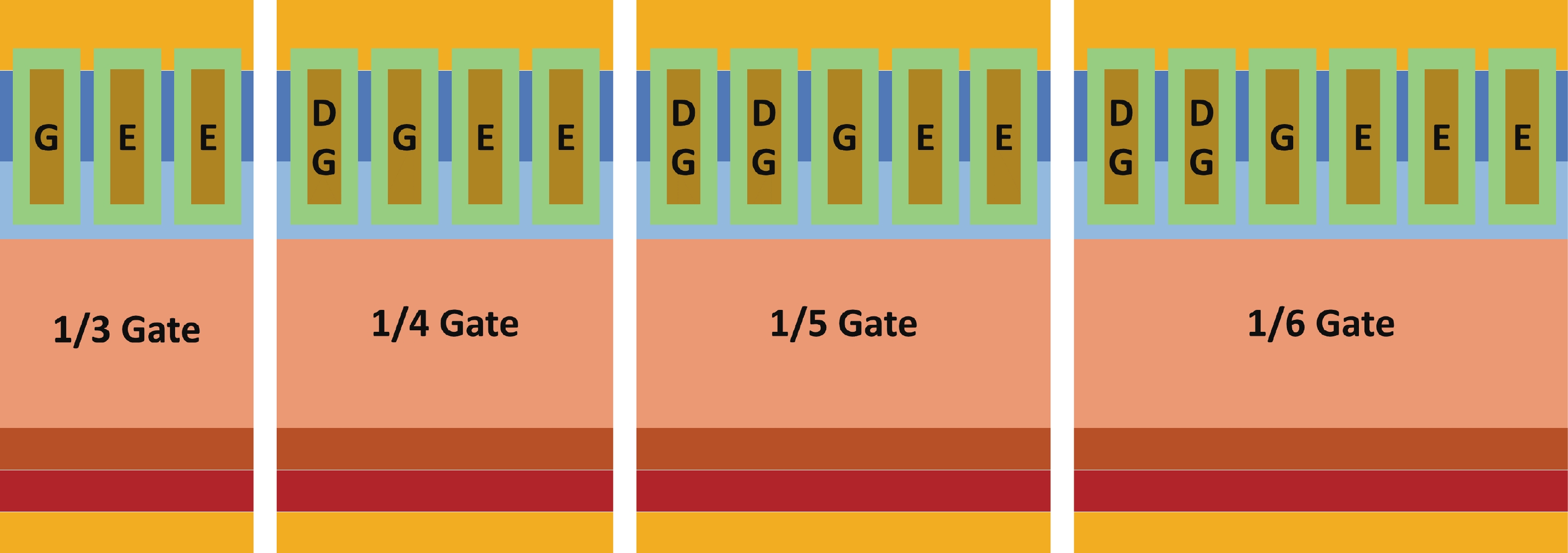
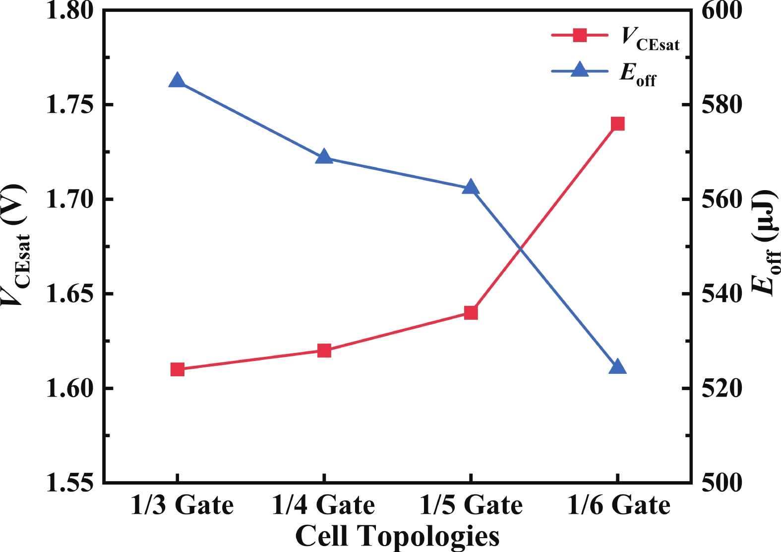
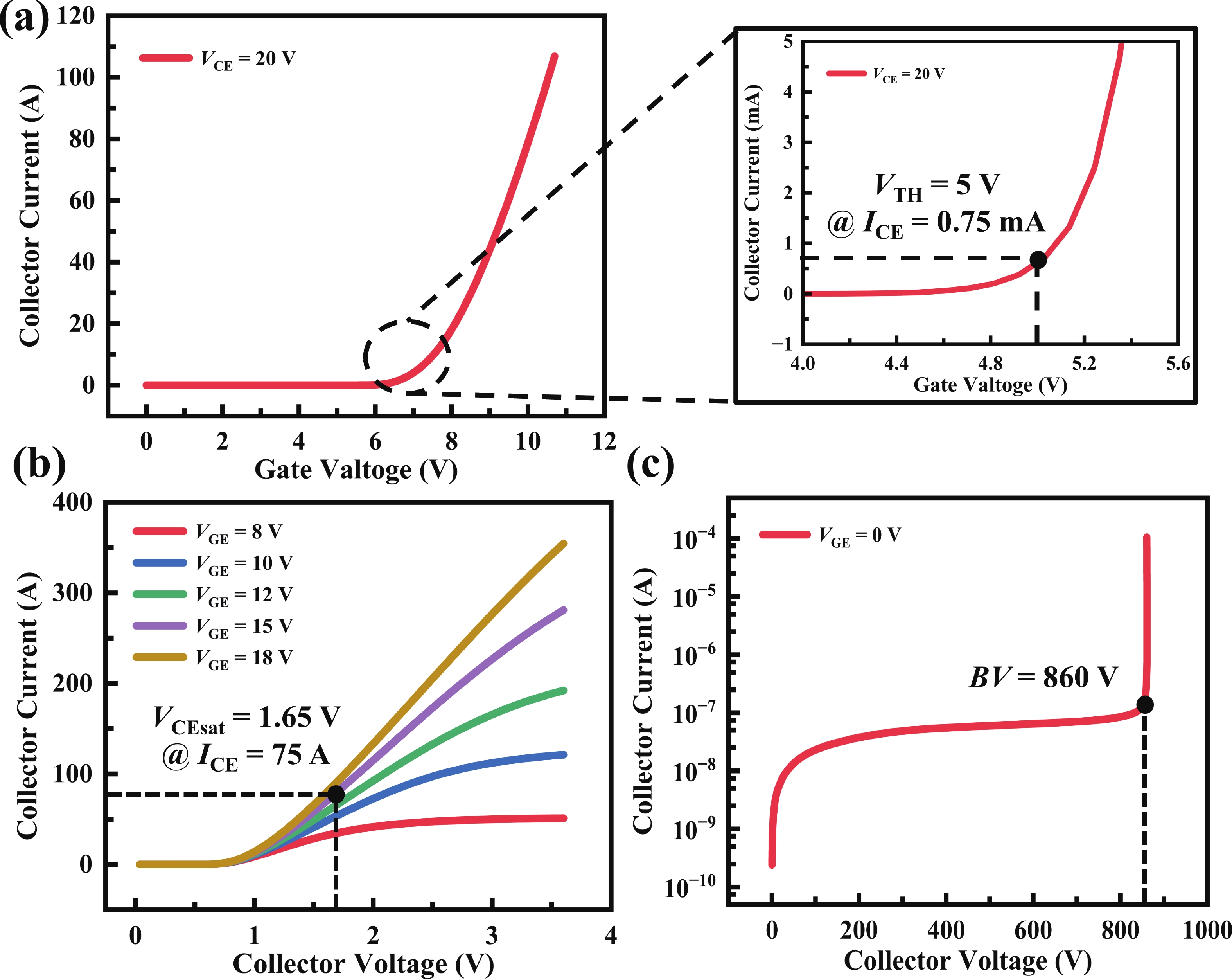
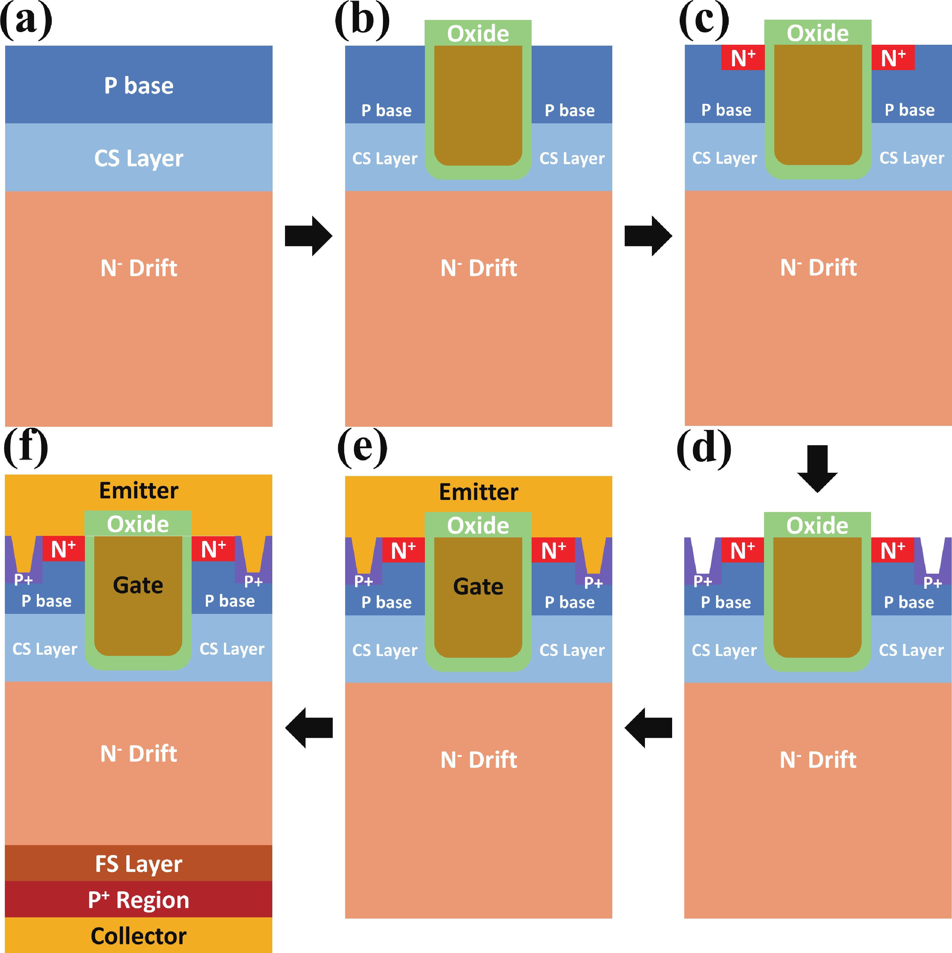
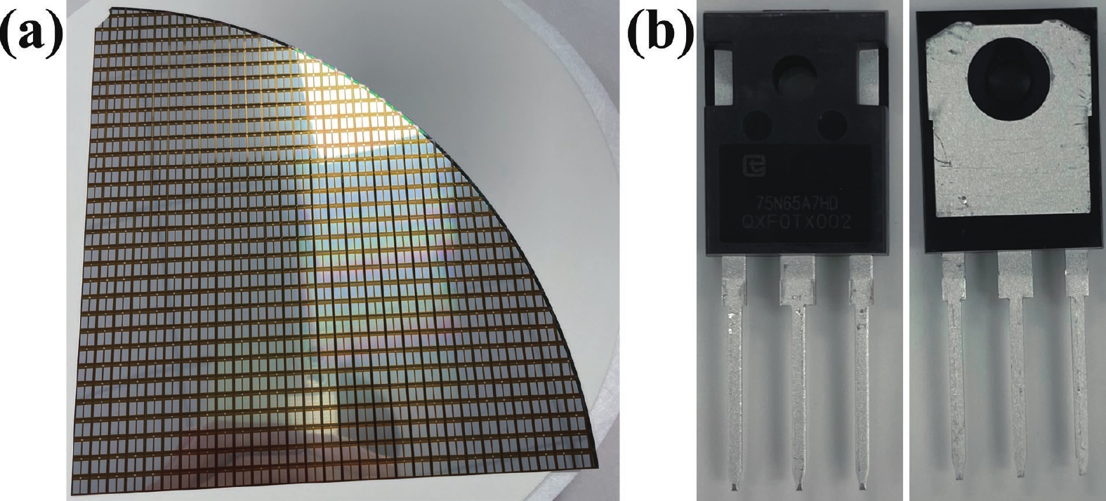
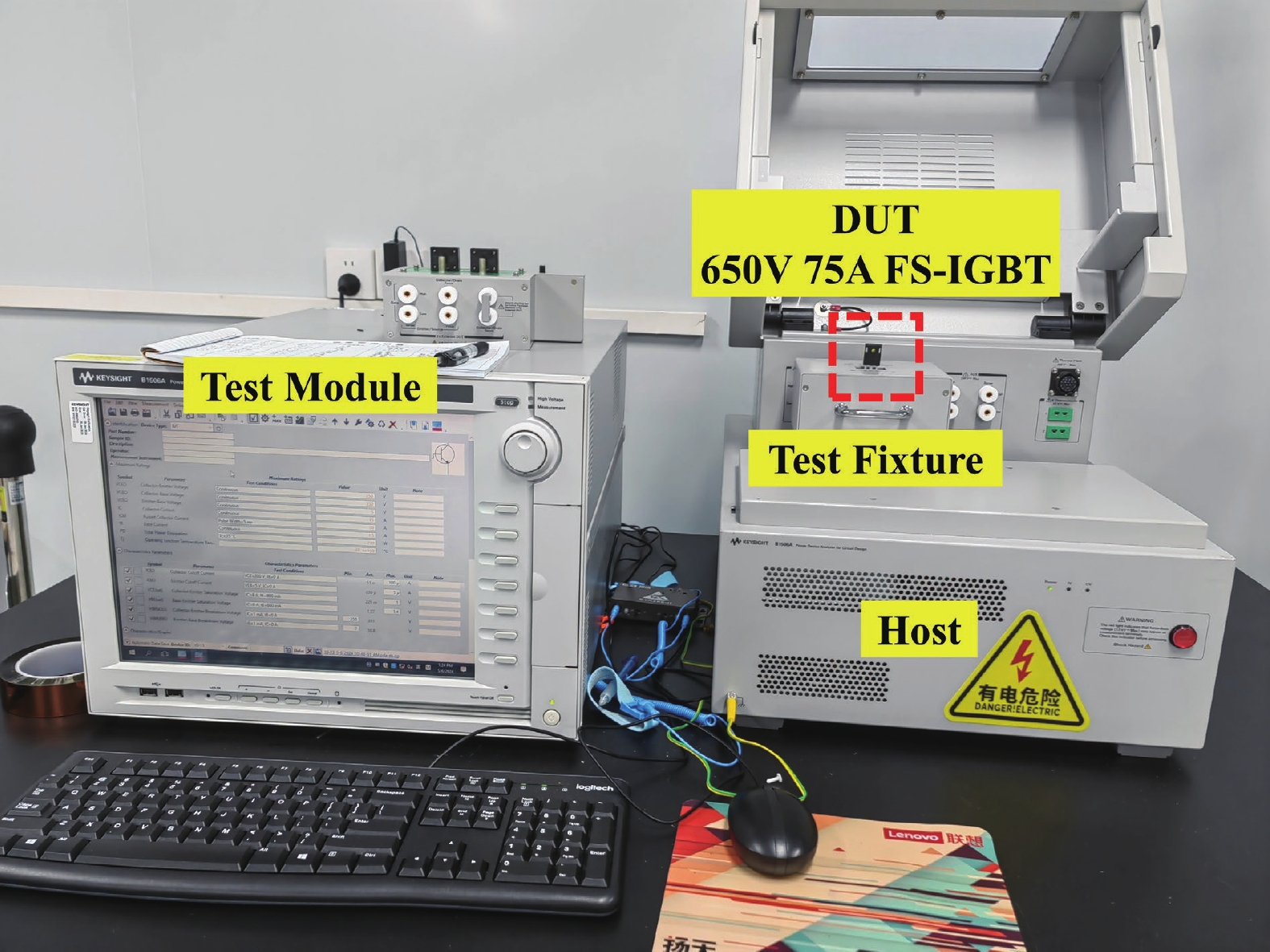
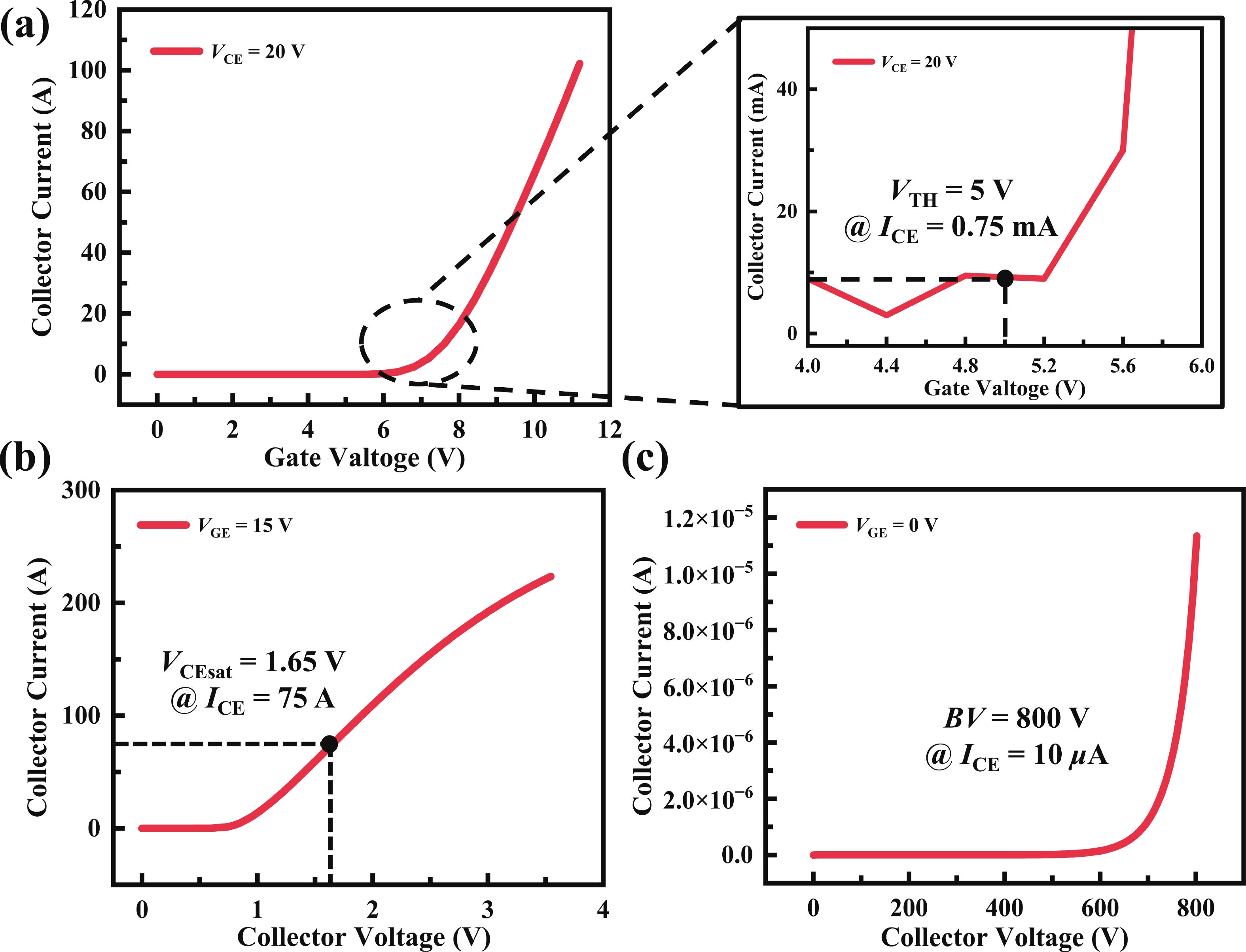
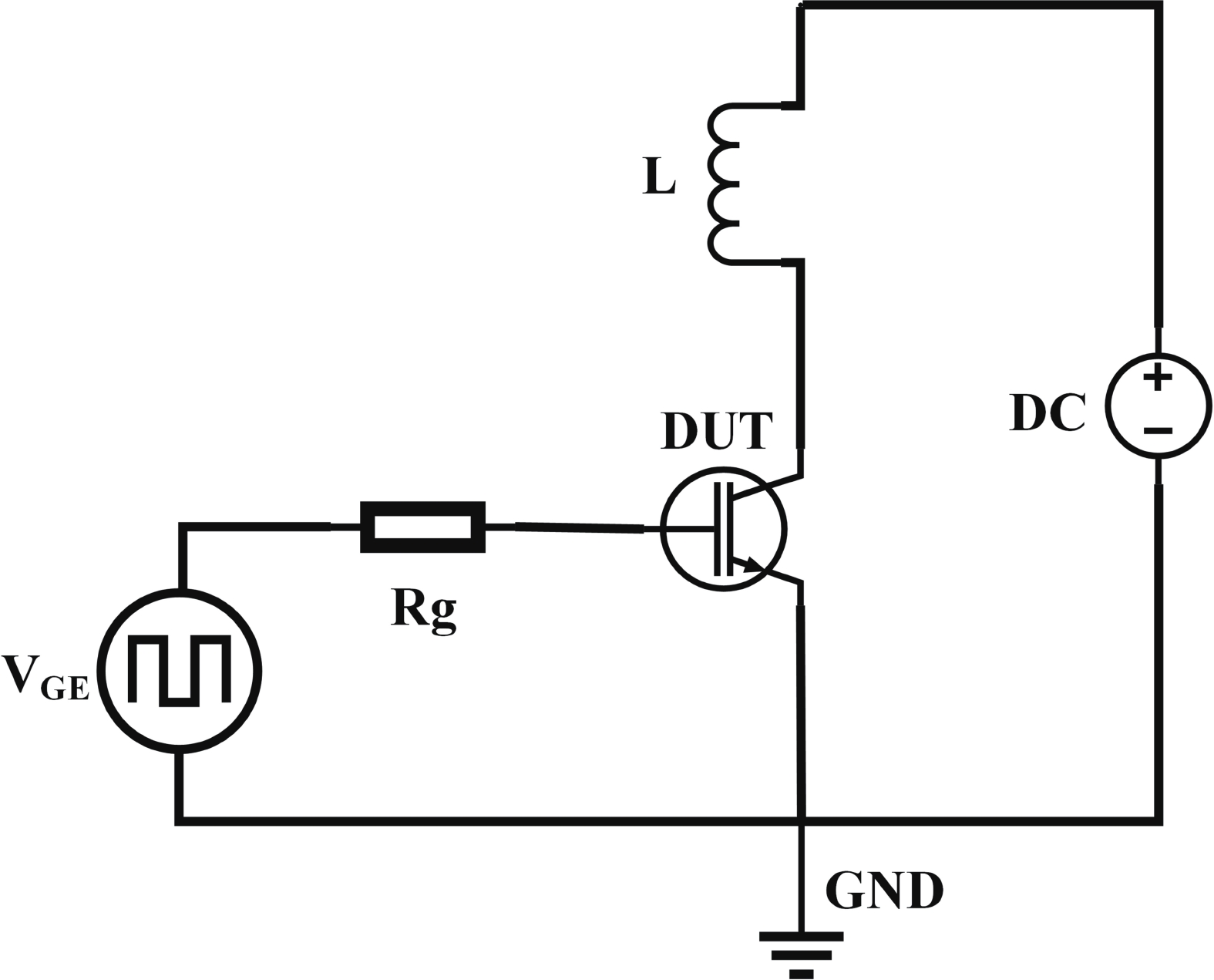
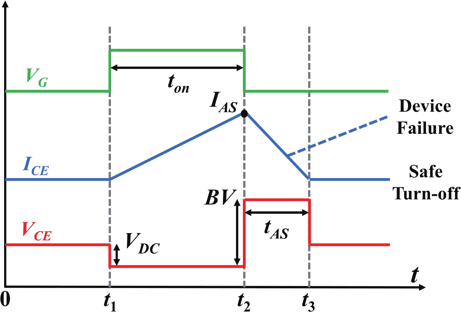
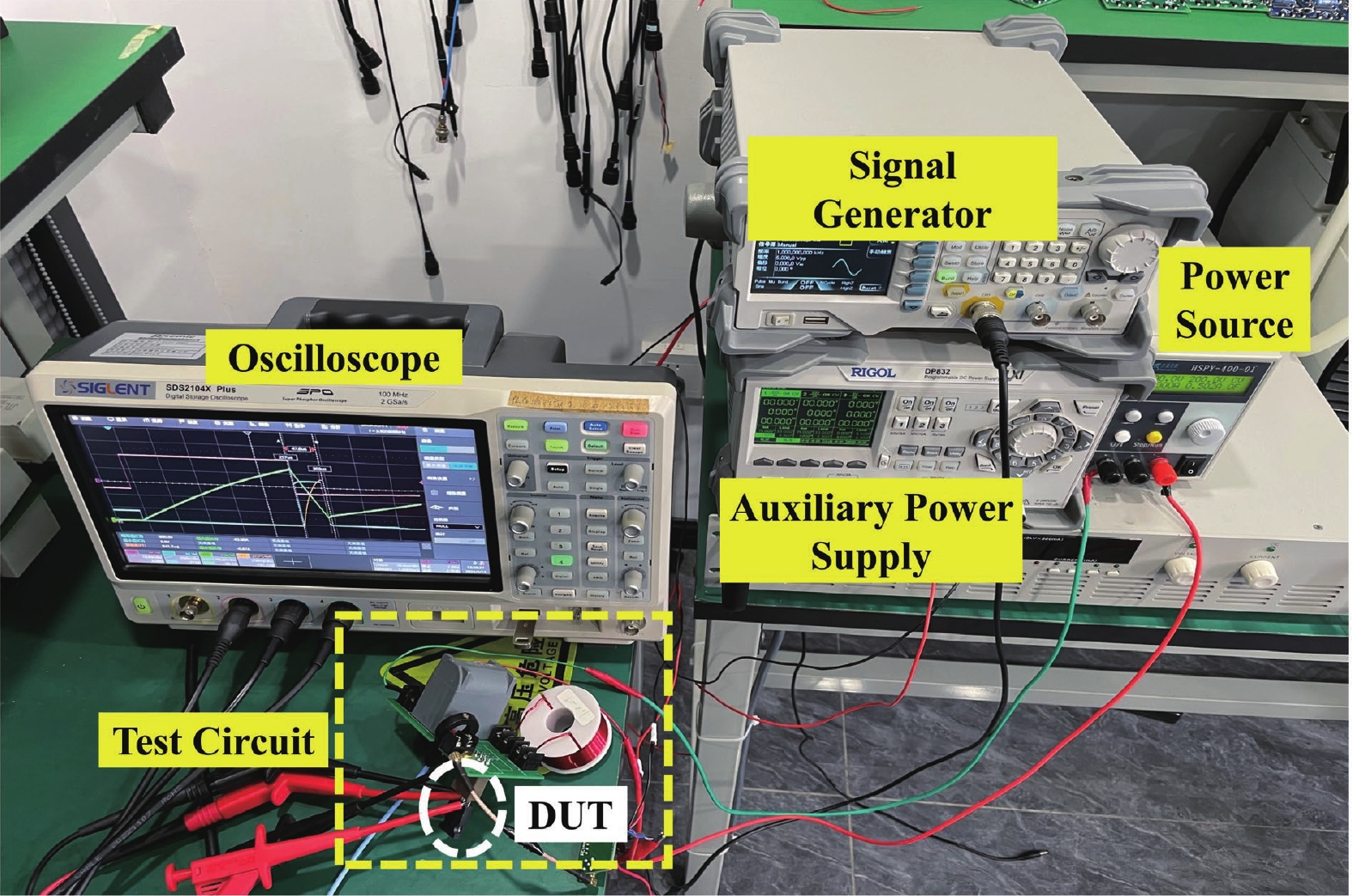
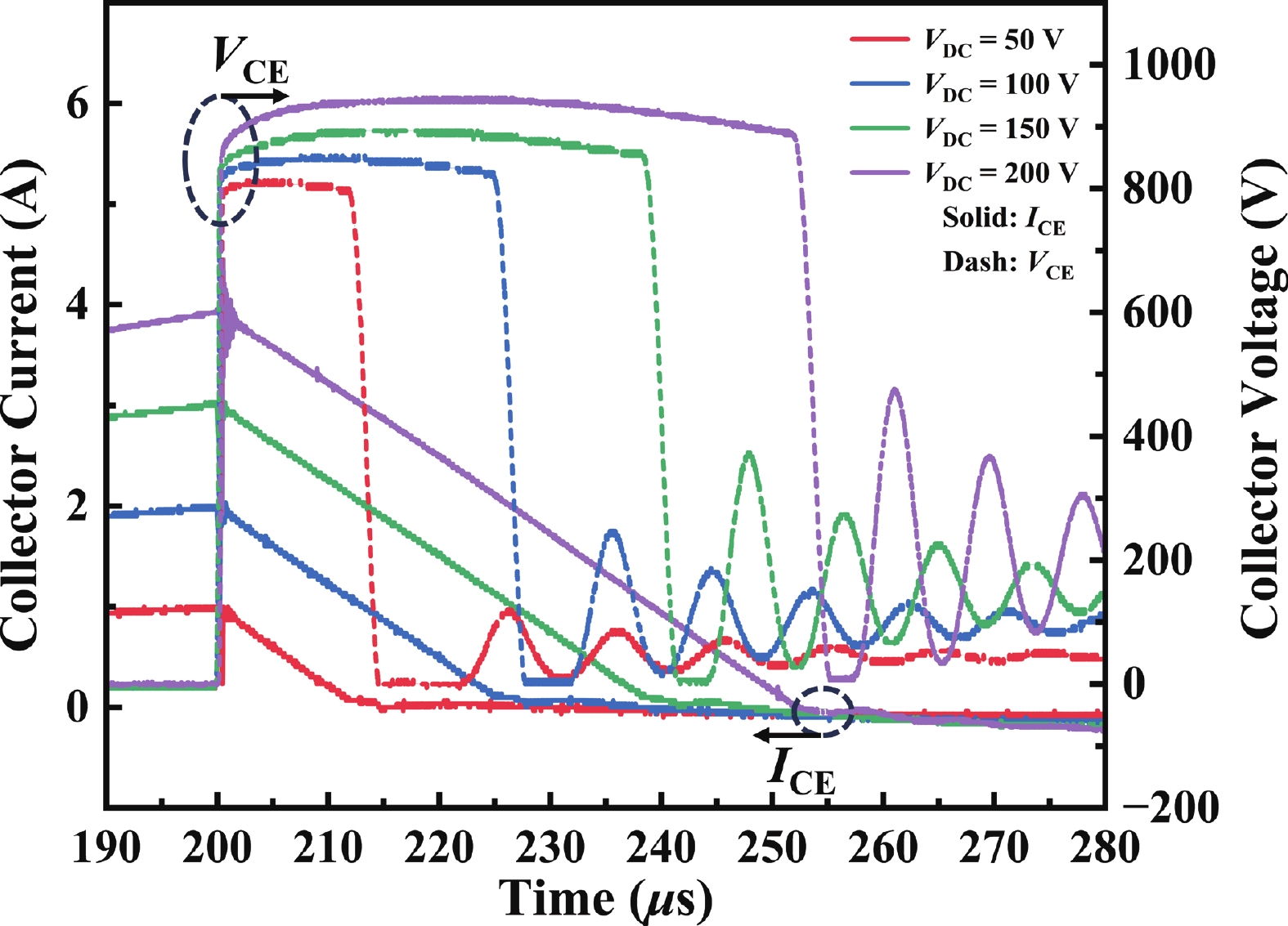
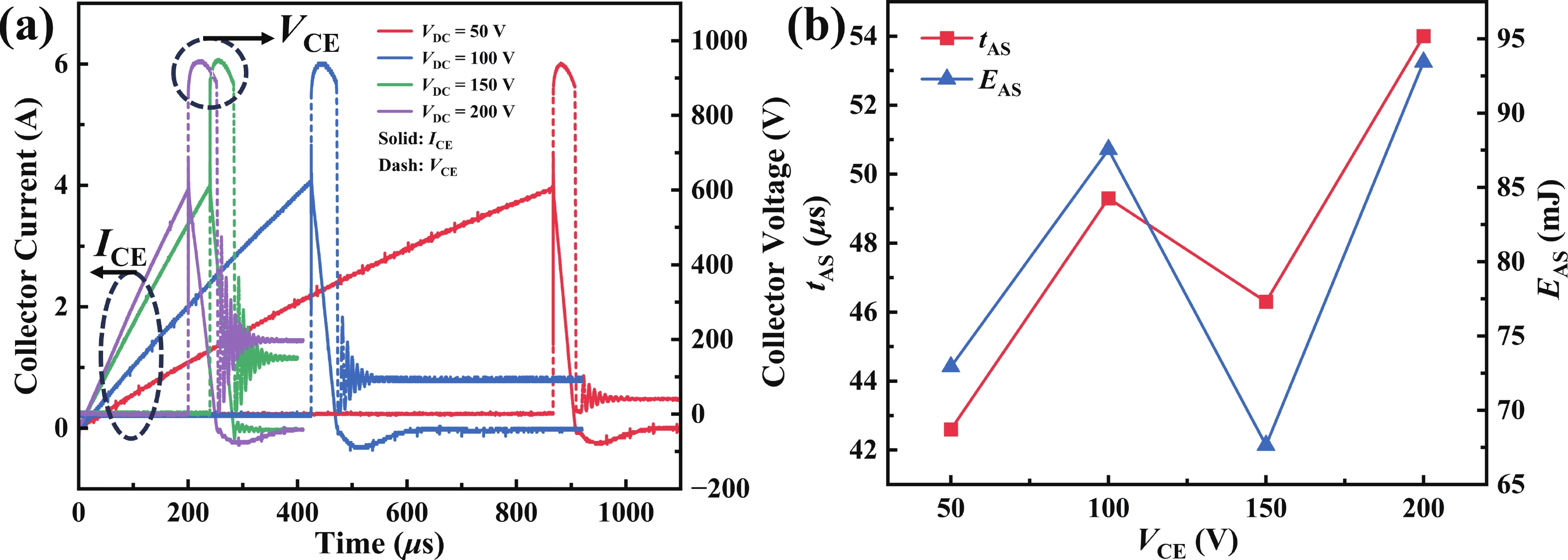
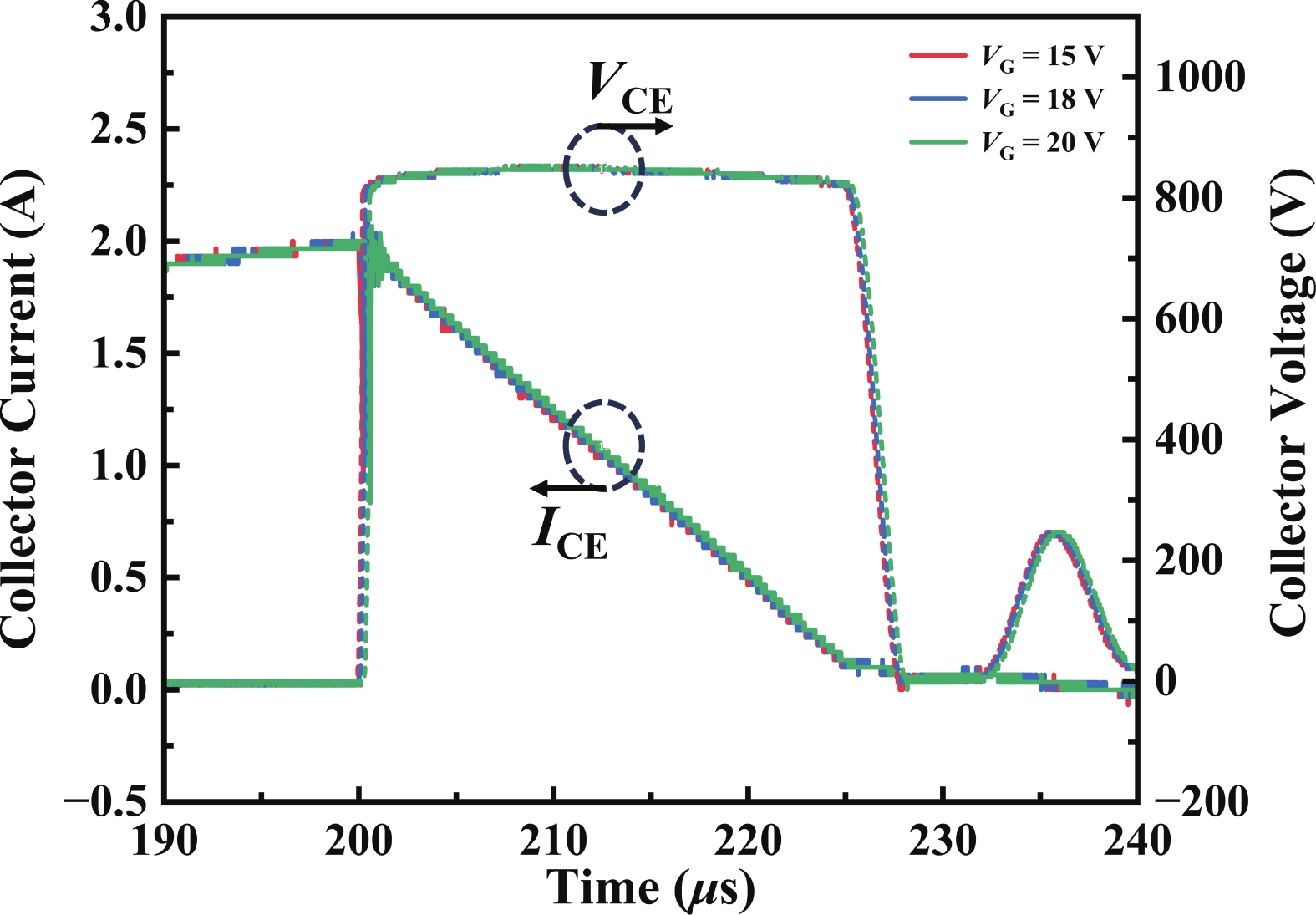
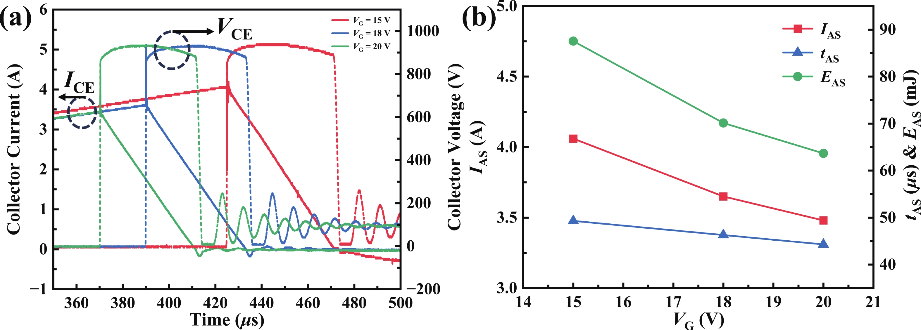
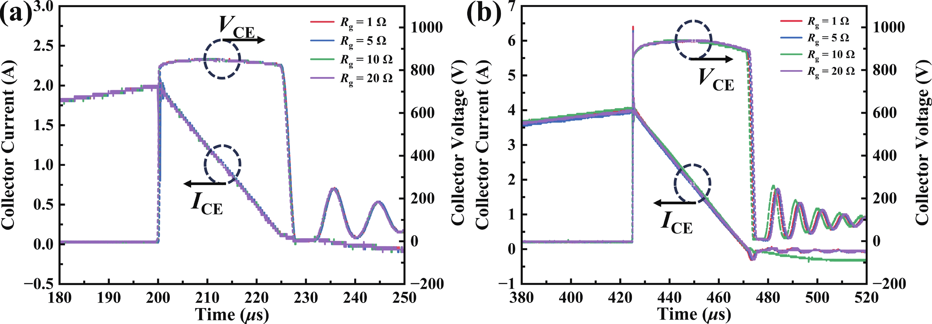
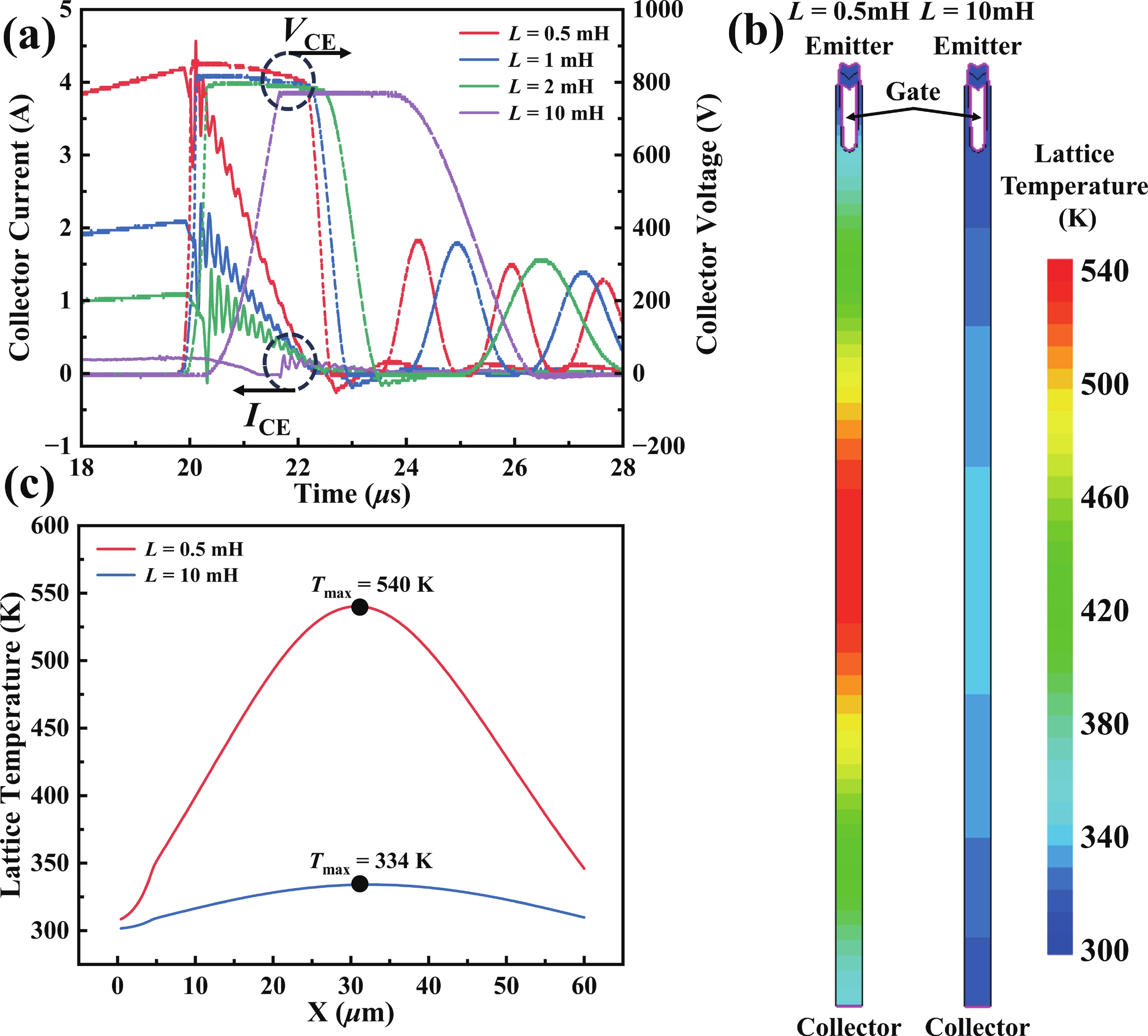
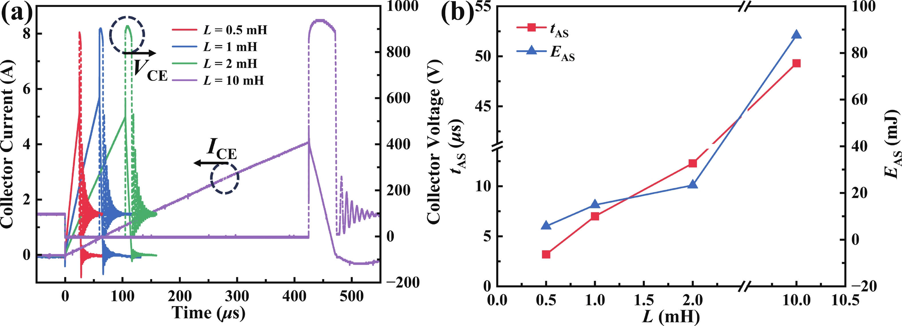
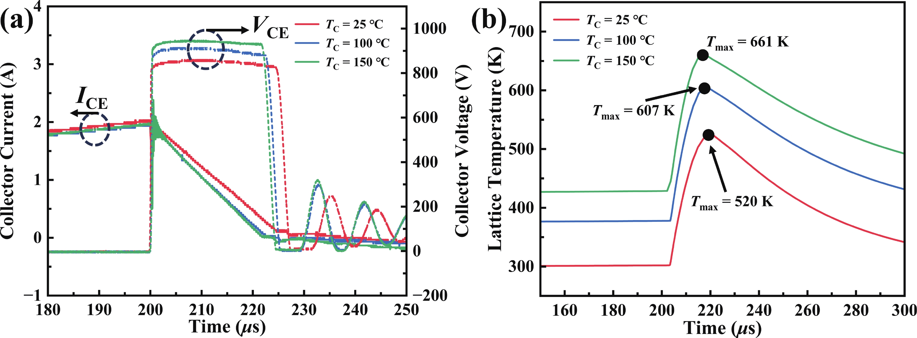
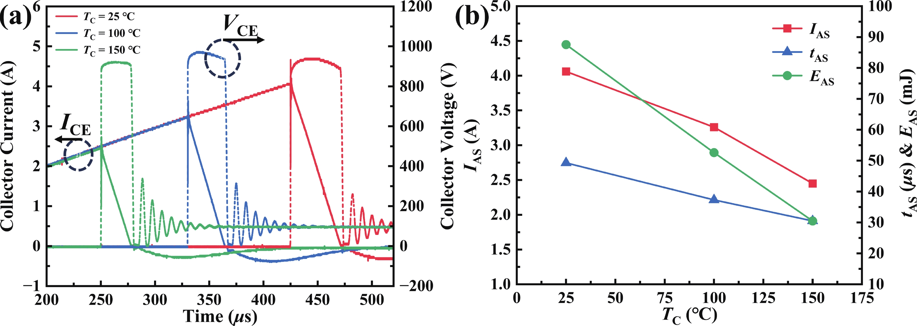
The dynamic avalanche effect is a critical factor influencing the performance and reliability of the field-stop insulated gate bipolar transistors (FS-IGBT). Unclamped inductive switching (UIS) is the primary method for testing the dynamic avalanche capability of FS-IGBTs. Numerous studies have demonstrated that factors such as device structure, avalanche-generating current filaments, and electrical parameters influence the dynamic avalanche effect of the FS-IGBT. However, few studies have focused on enhancing the avalanche reliability of the FS-IGBT by adjusting circuit parameters during operation. In this paper, the dynamic avalanche effect of the FS-IGBT under UIS conditions is comprehensively investigated through a series of comparative experiments with varying circuit parameters, including bus voltage VDC, gate voltage VG, gate resistance Rg, load inductance L, and temperature TC. Furthermore, a method to enhance the dynamic avalanche reliability of the FS-IGBT under UIS by optimizing circuit parameters is proposed. In practical applications, reducing gate voltage, increasing load inductance, and lowering temperature can effectively improve the dynamic avalanche capability of the FS-IGBT.
J. Semicond.
2025, 46(9): 092201 doi: 10.1088/1674-4926/25020010
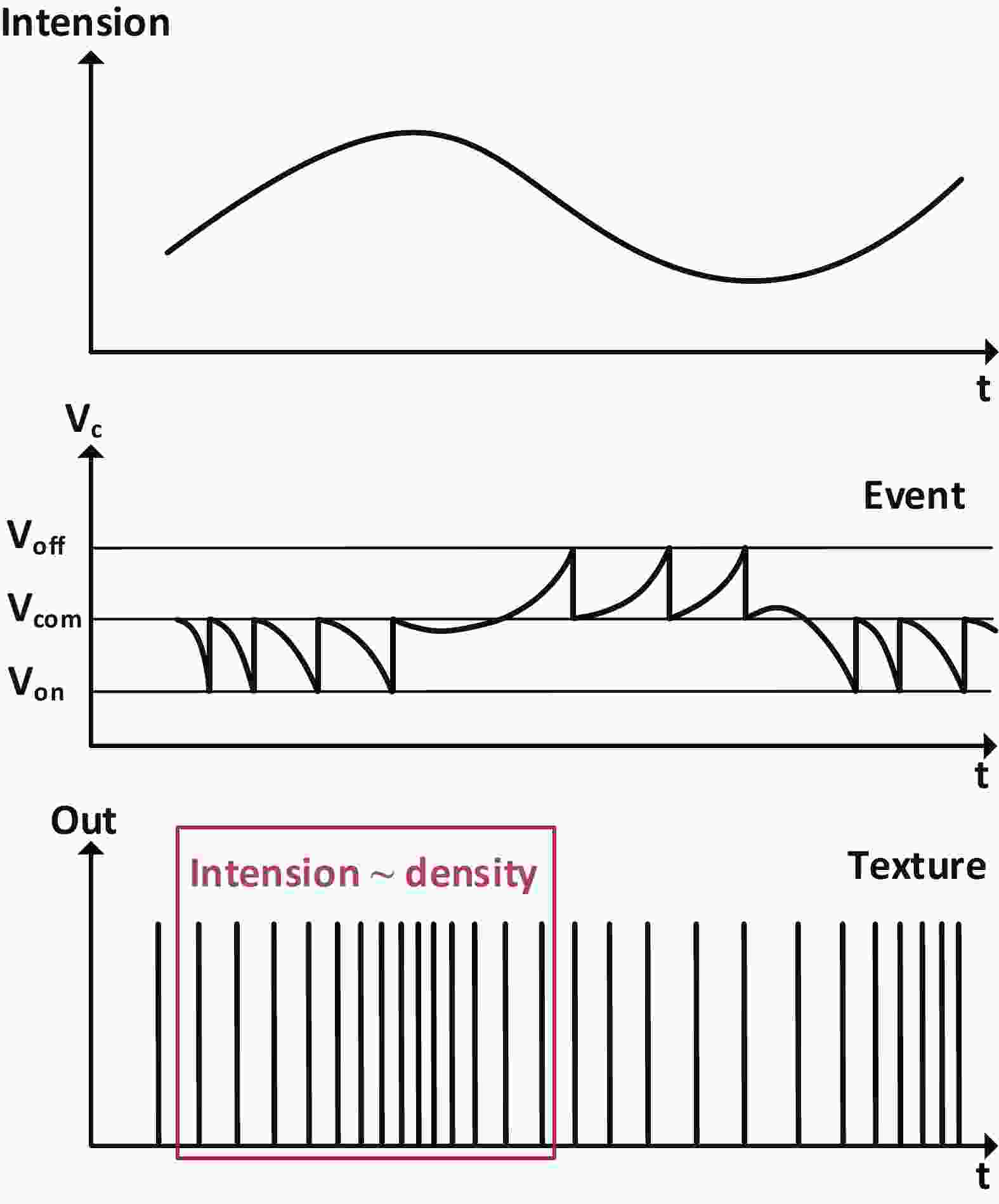
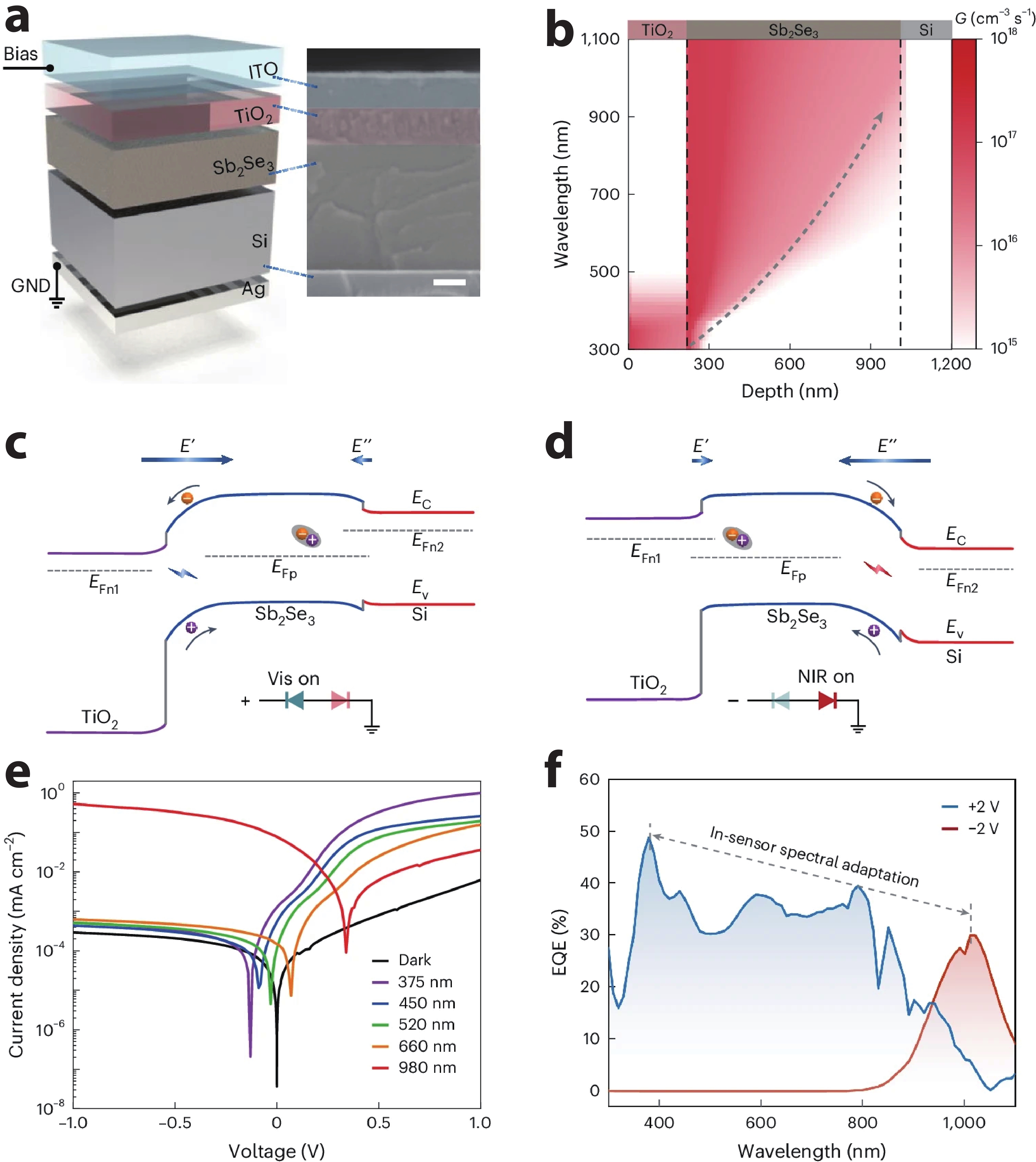
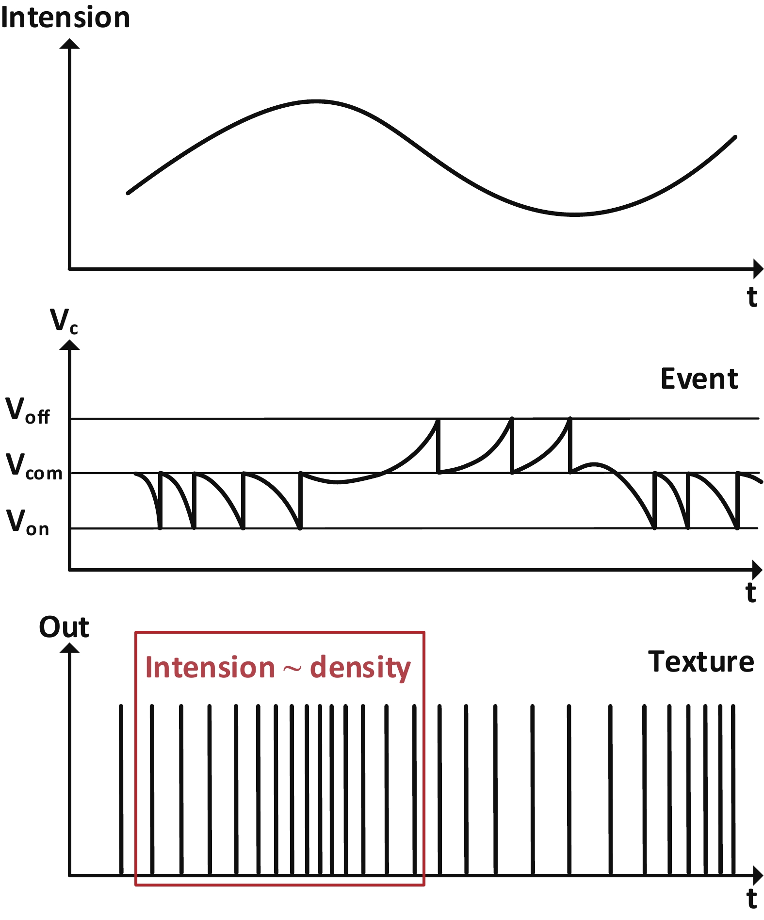
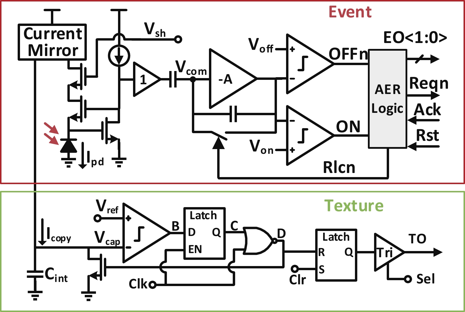
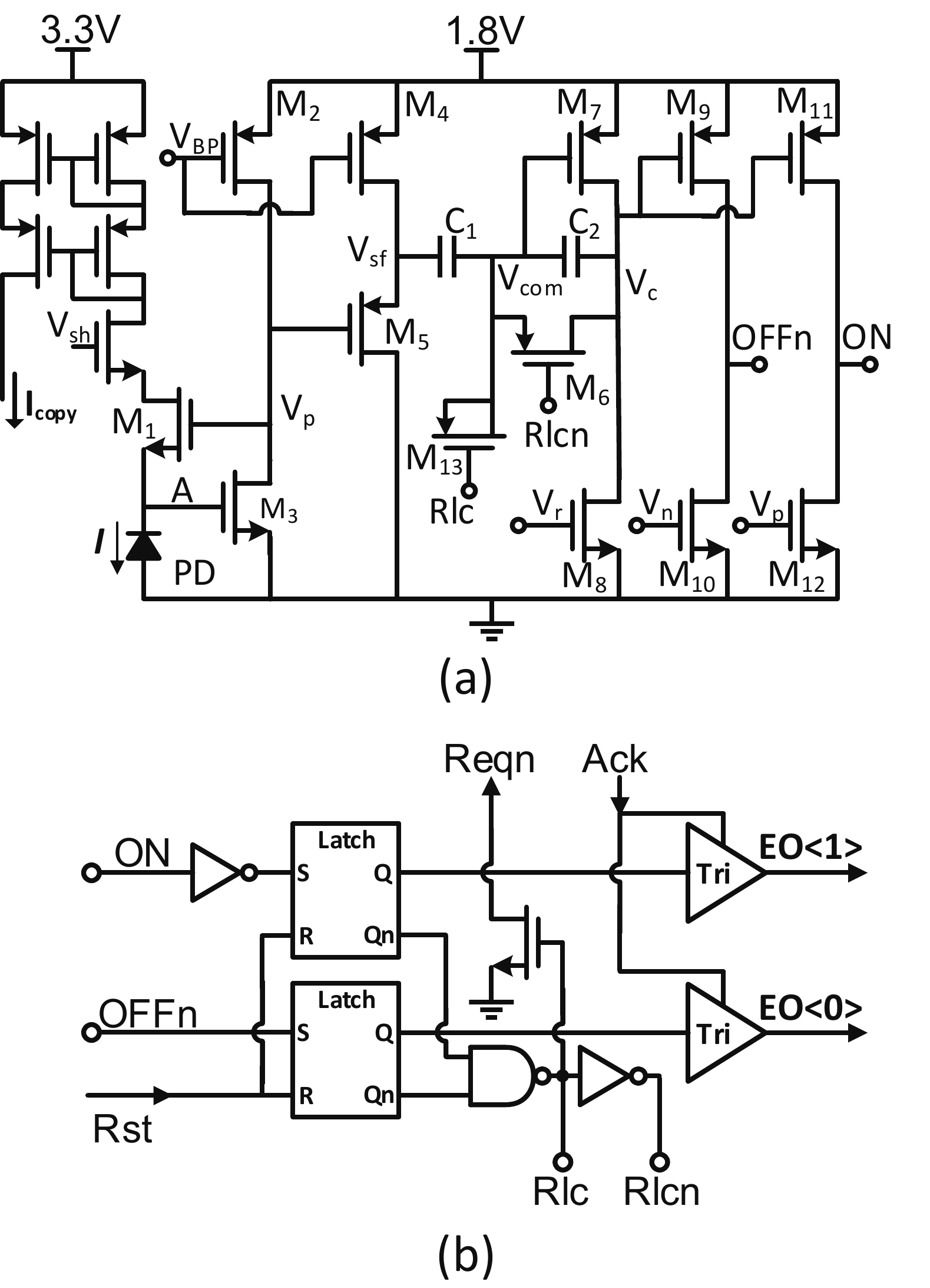
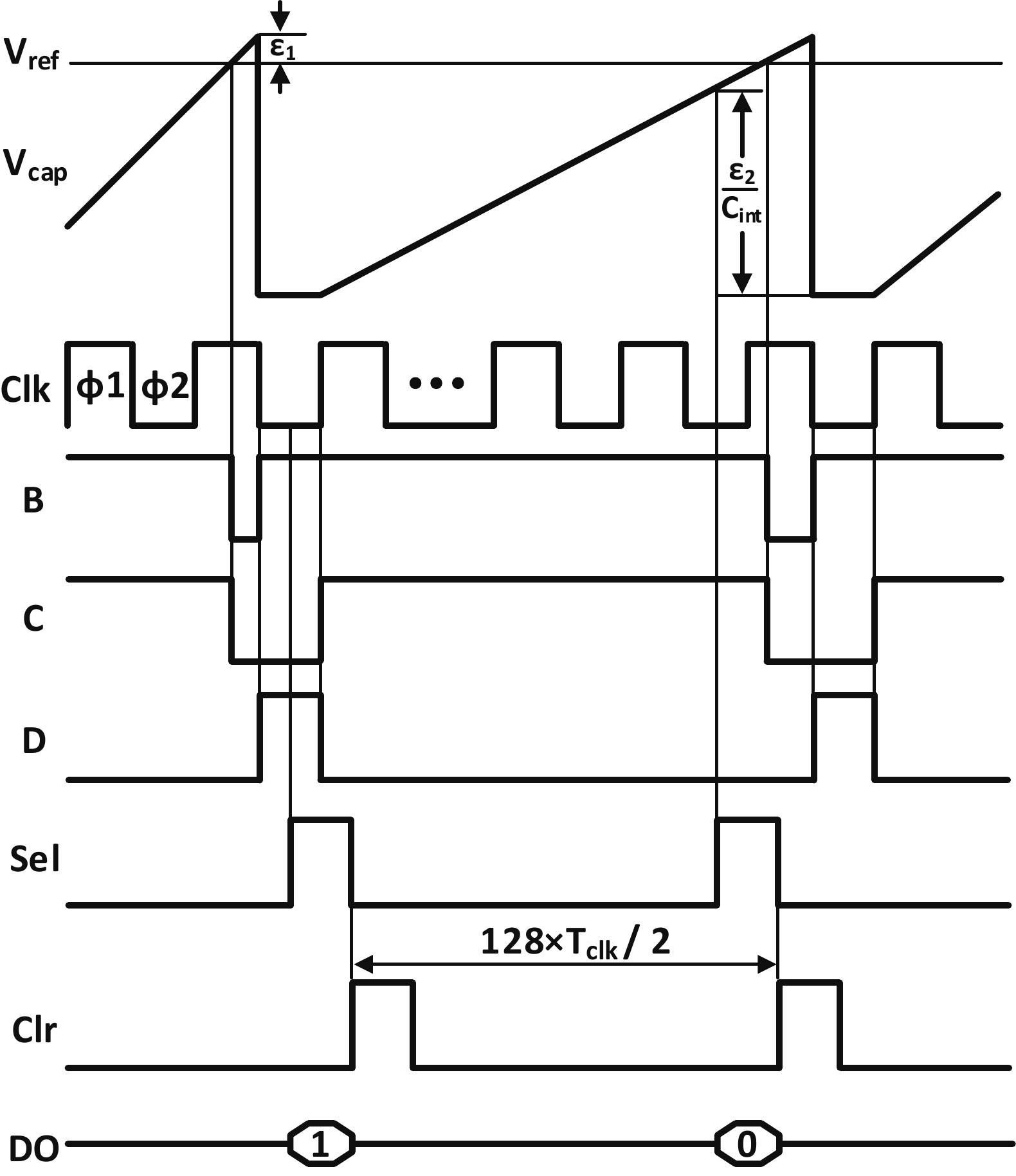
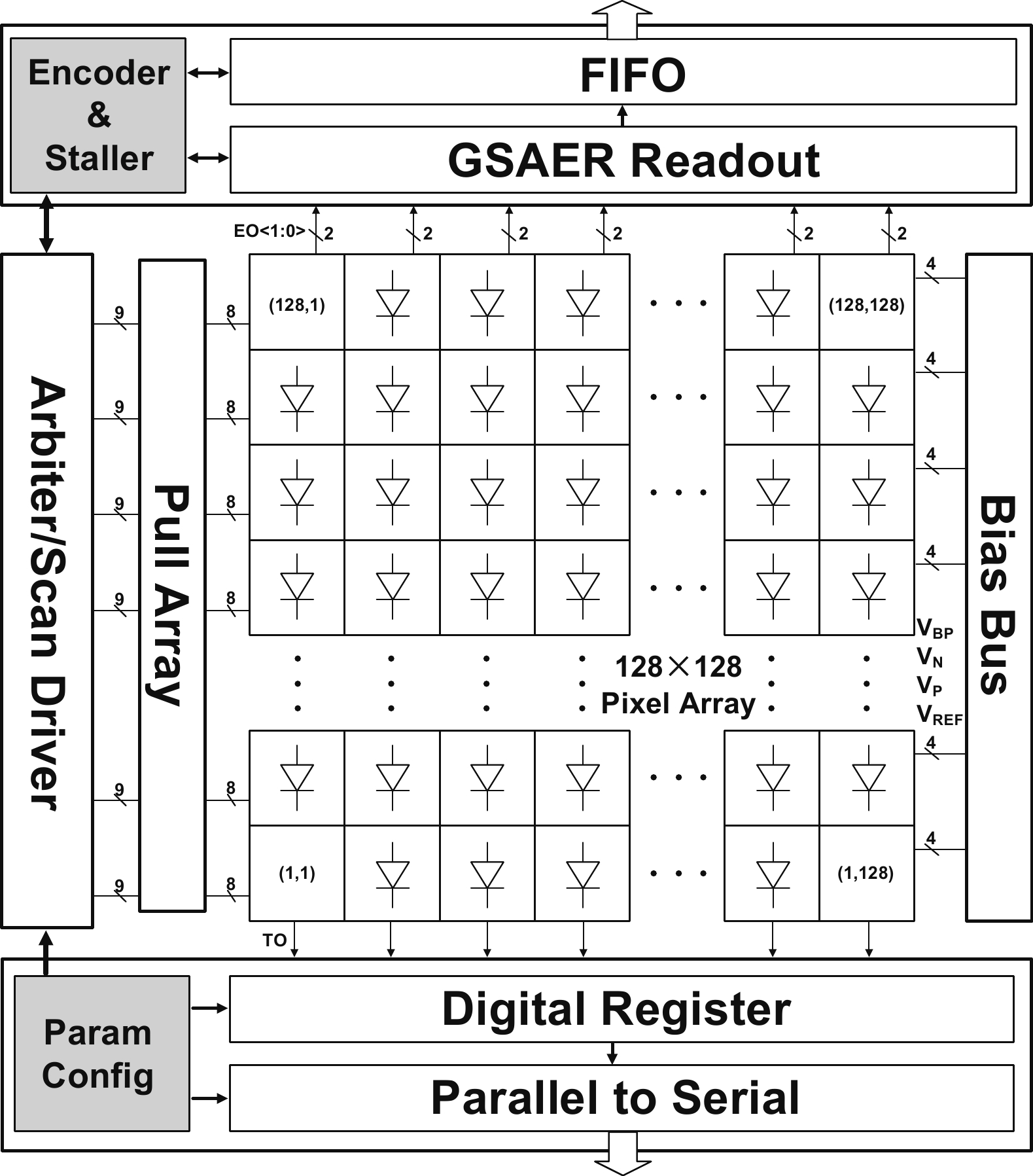
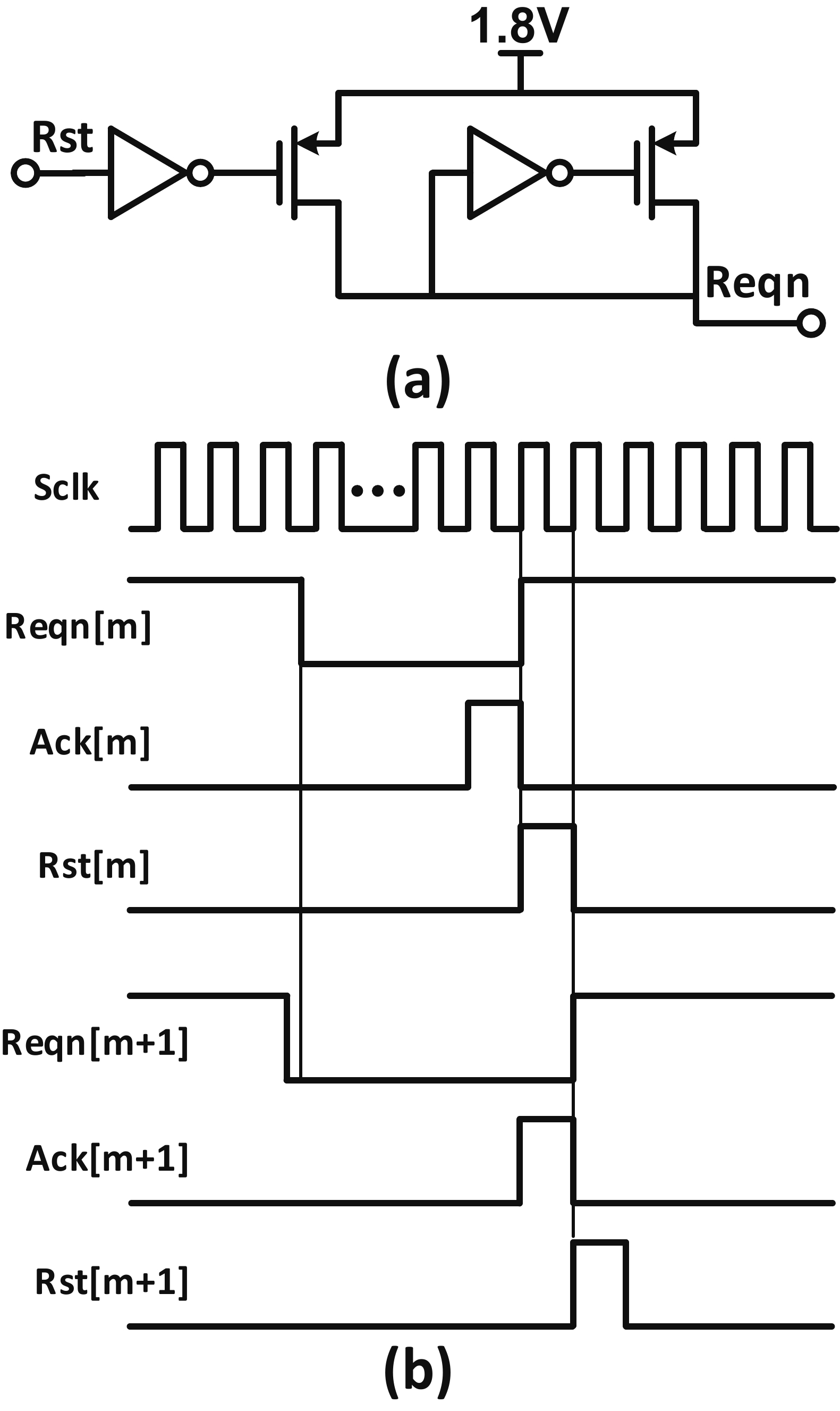
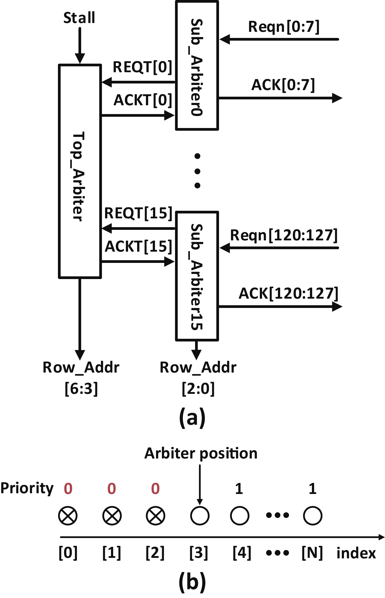
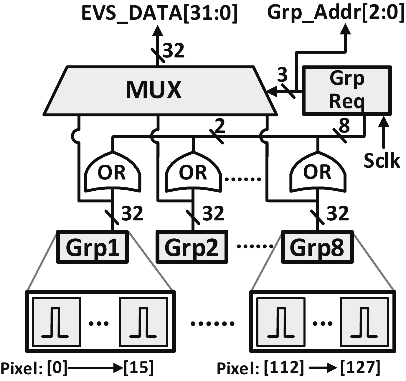
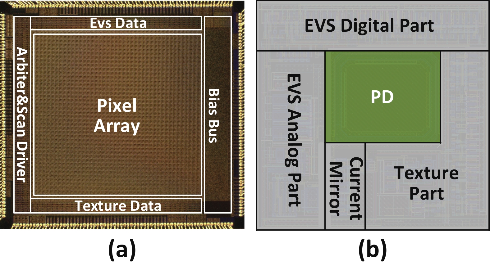
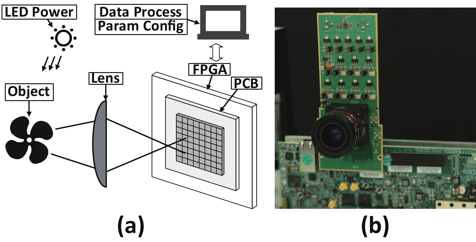
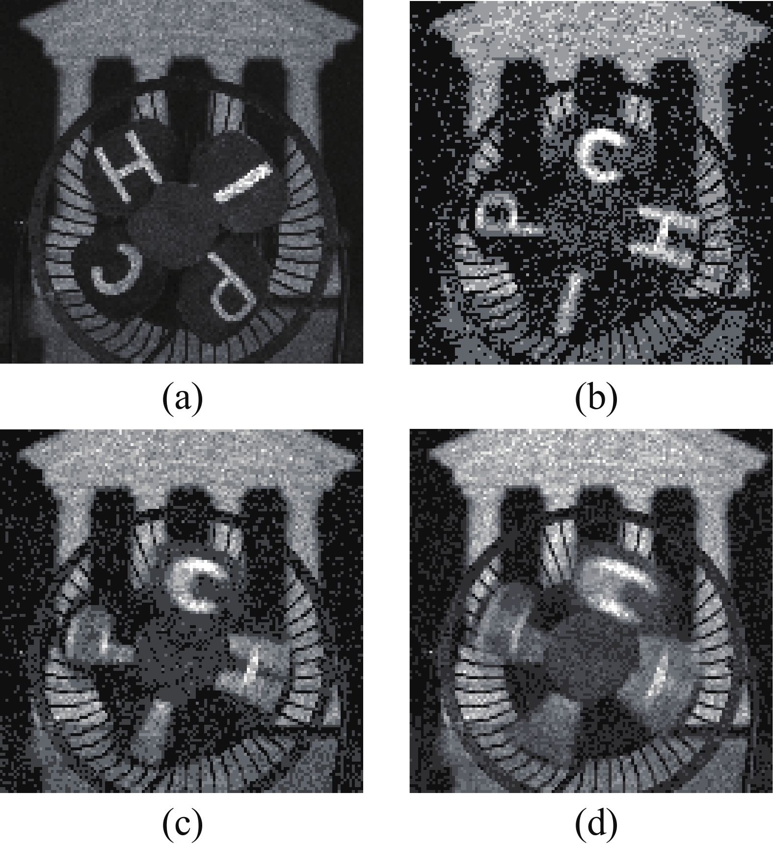
The event-based vision sensor (EVS), which can generate efficient spiking data streams by exclusively detecting motion, exemplifies neuromorphic vision methodologies. Generally, its inherent lack of texture features limits effectiveness in complex vision processing tasks, necessitating supplementary visual information. However, to date, no event-based hybrid vision solution has been developed that preserves the characteristics of complete spike data streams to support synchronous computation architectures based on spiking neural network (SNN). In this paper, we present a novel spike-based sensor with digitized pixels, which integrates the event detection structure with the pulse frequency modulation (PFM) circuit. This design enables the simultaneous output of spiking data that encodes both temporal changes and texture information. Fabricated in 180 nm process, the proposed sensor achieves a resolution of 128 × 128, a maximum event rate of 960 Meps, a grayscale frame rate of 117.1 kfps, and a measured power consumption of 60.1 mW, which is suited for high-speed, low-latency, edge SNN-based vision computing systems.
J. Semicond.
2025, 46(9): 092501 doi: 10.1088/1674-4926/25010026
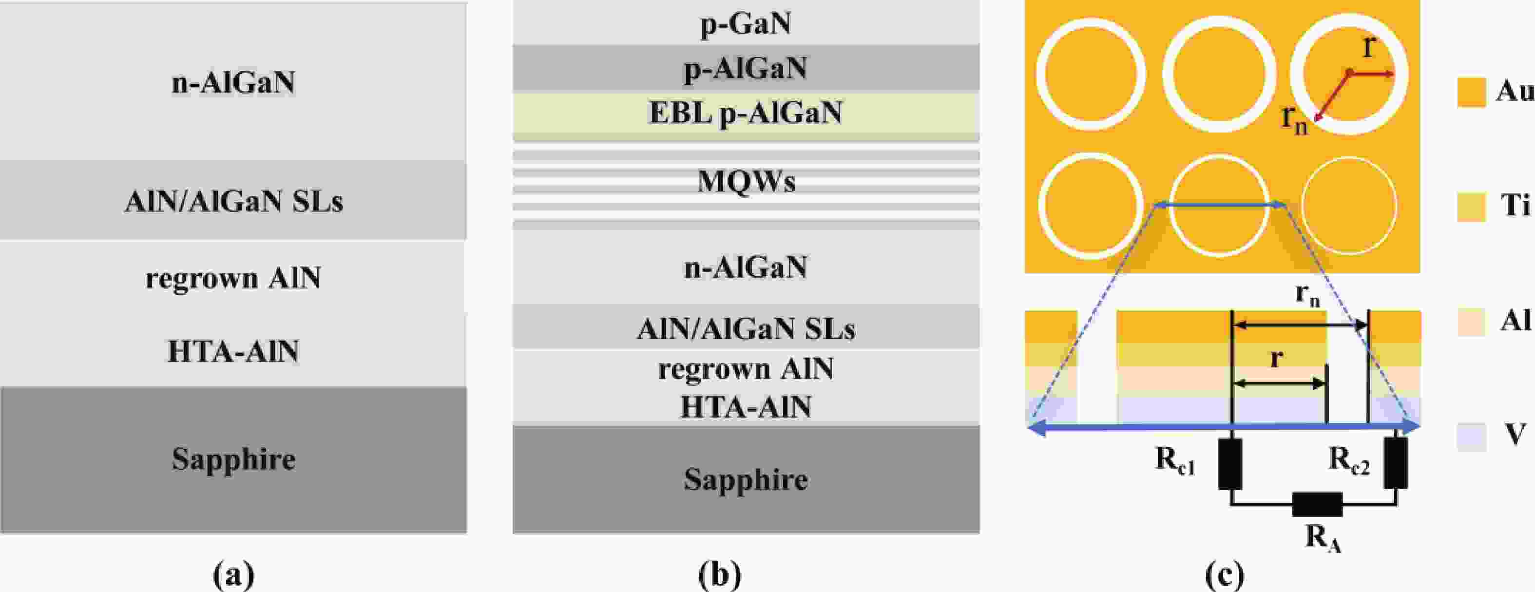
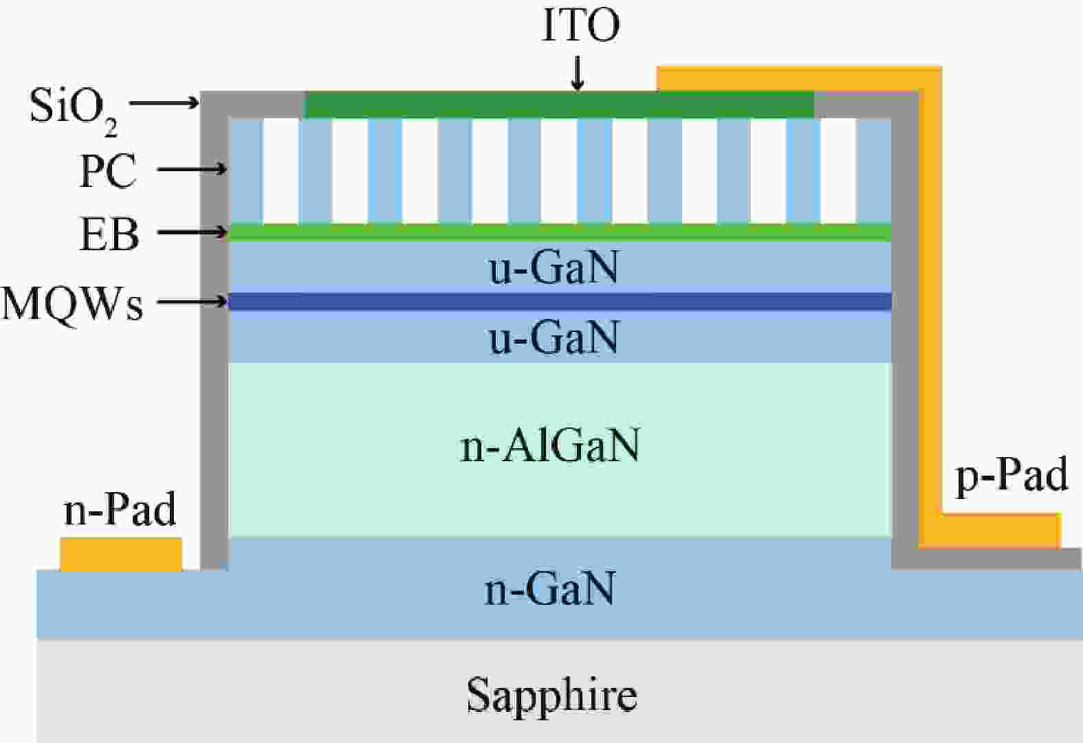
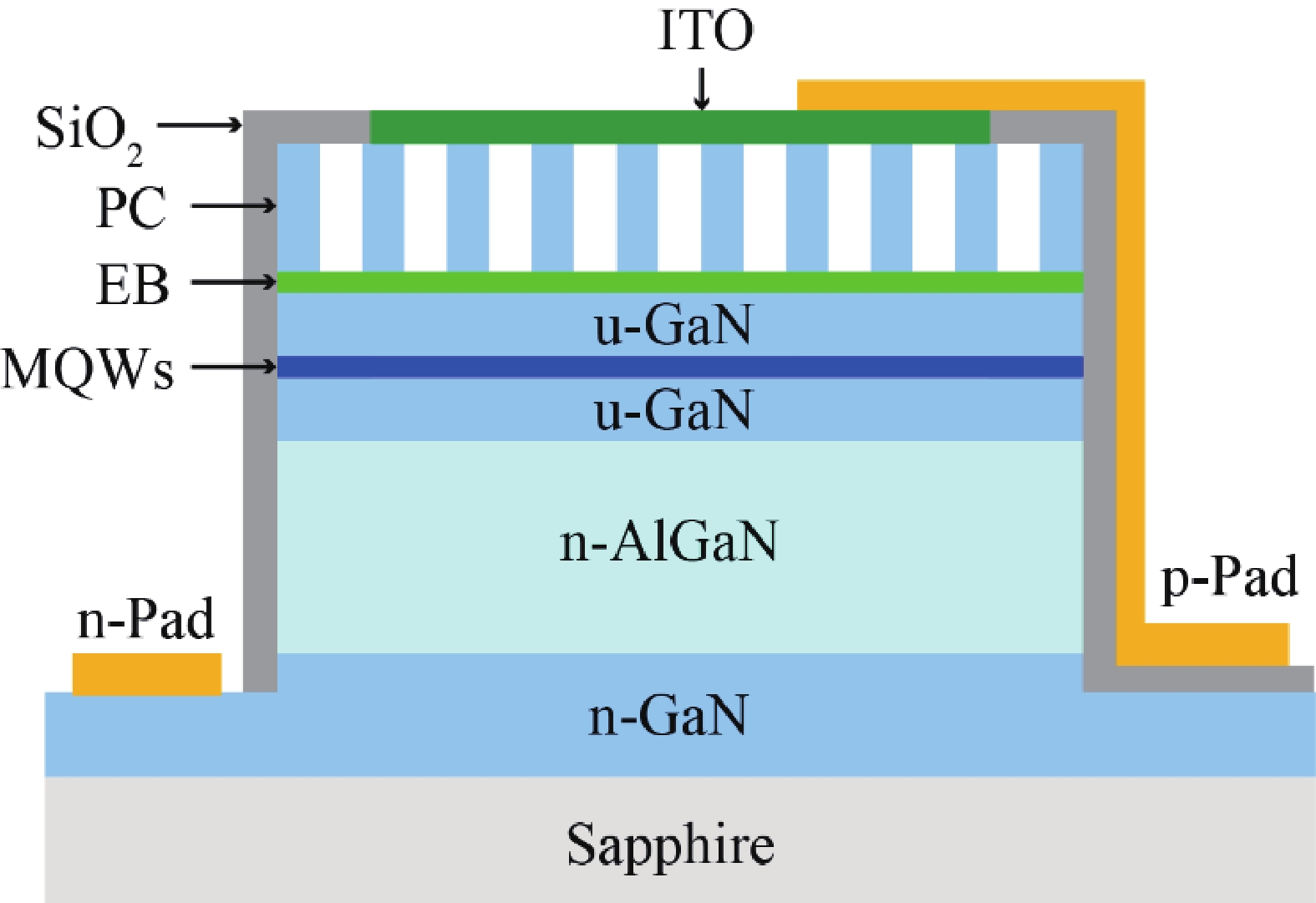
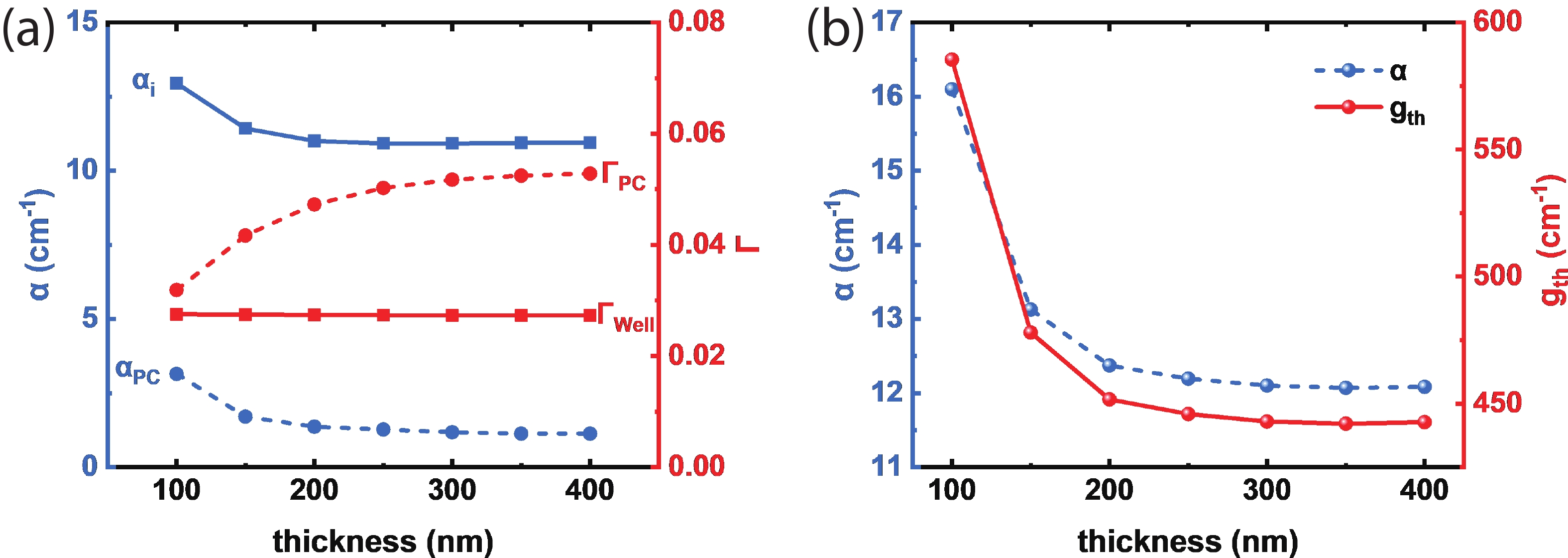
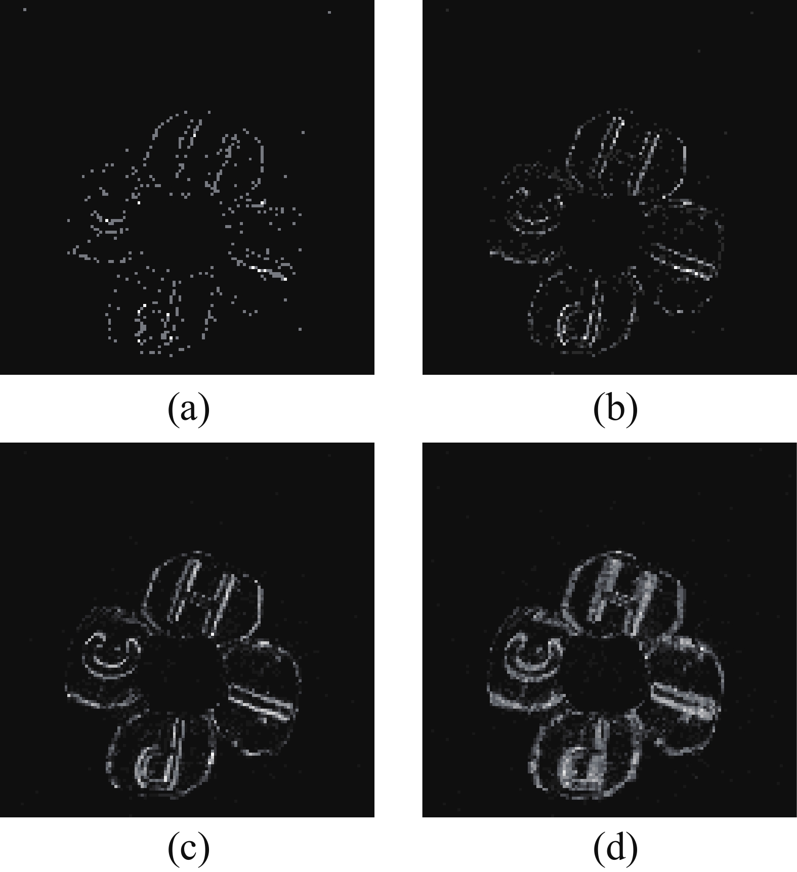
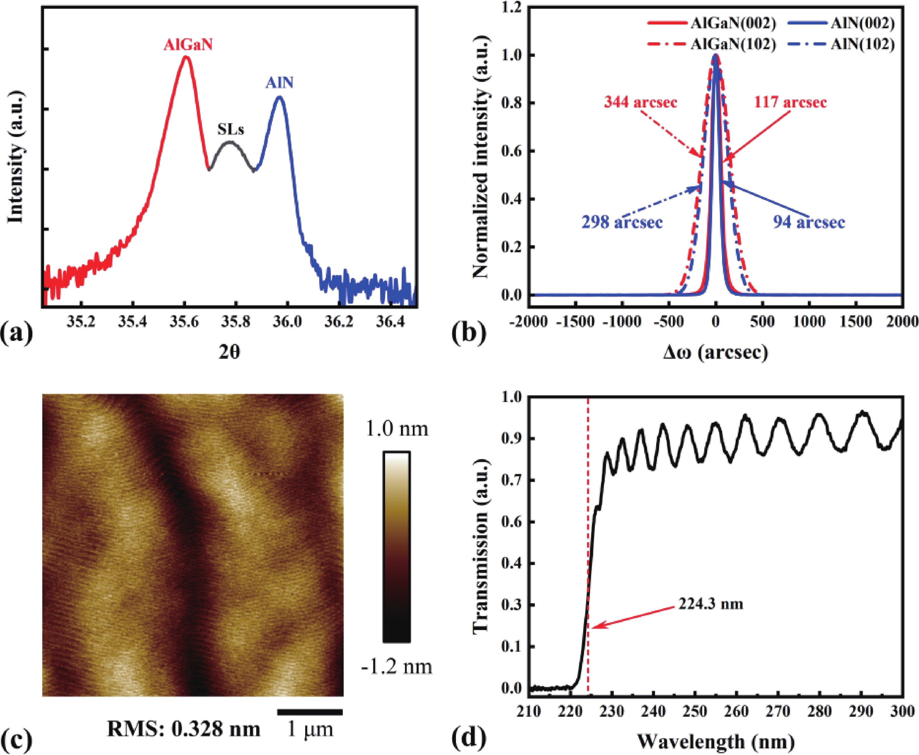
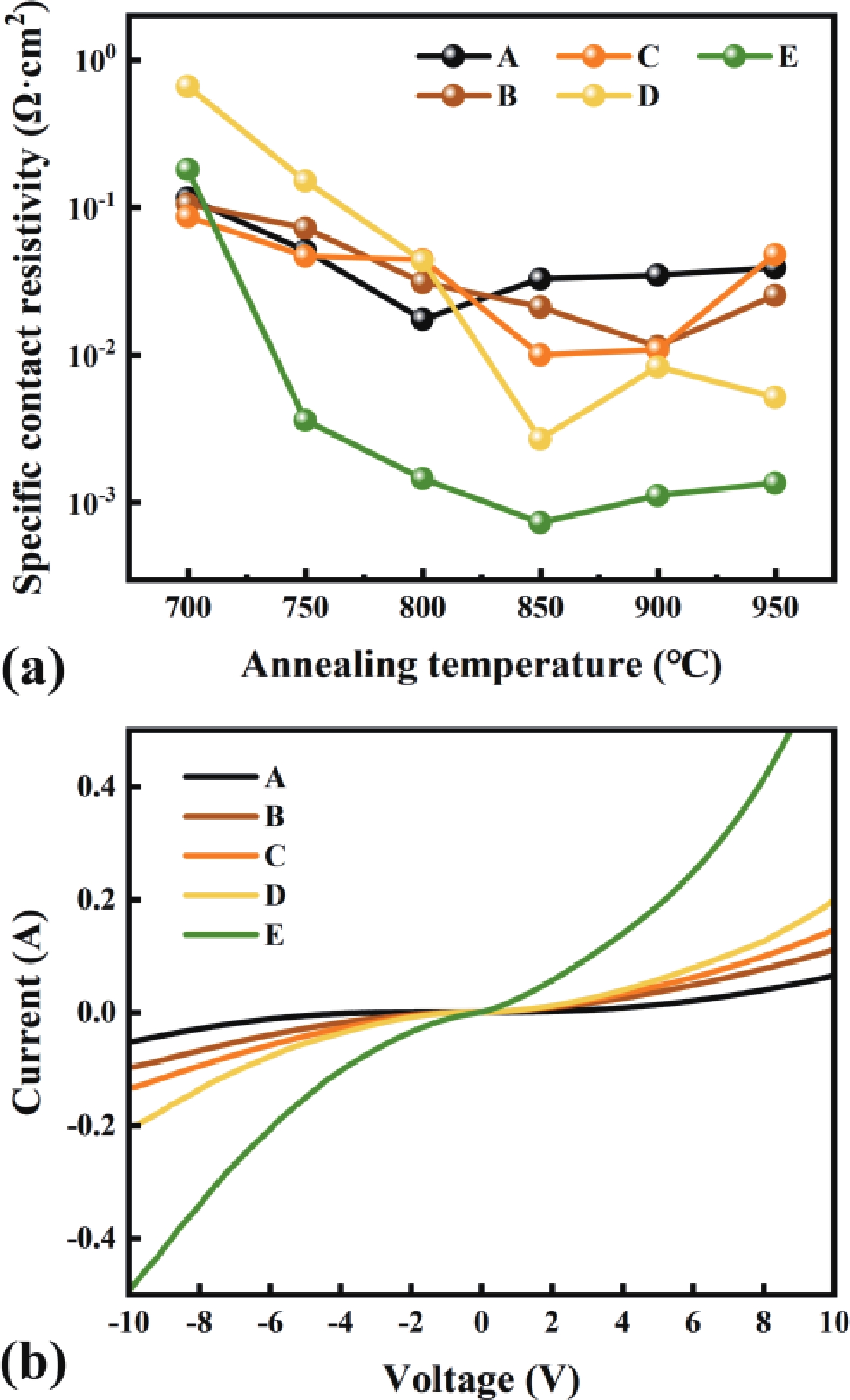
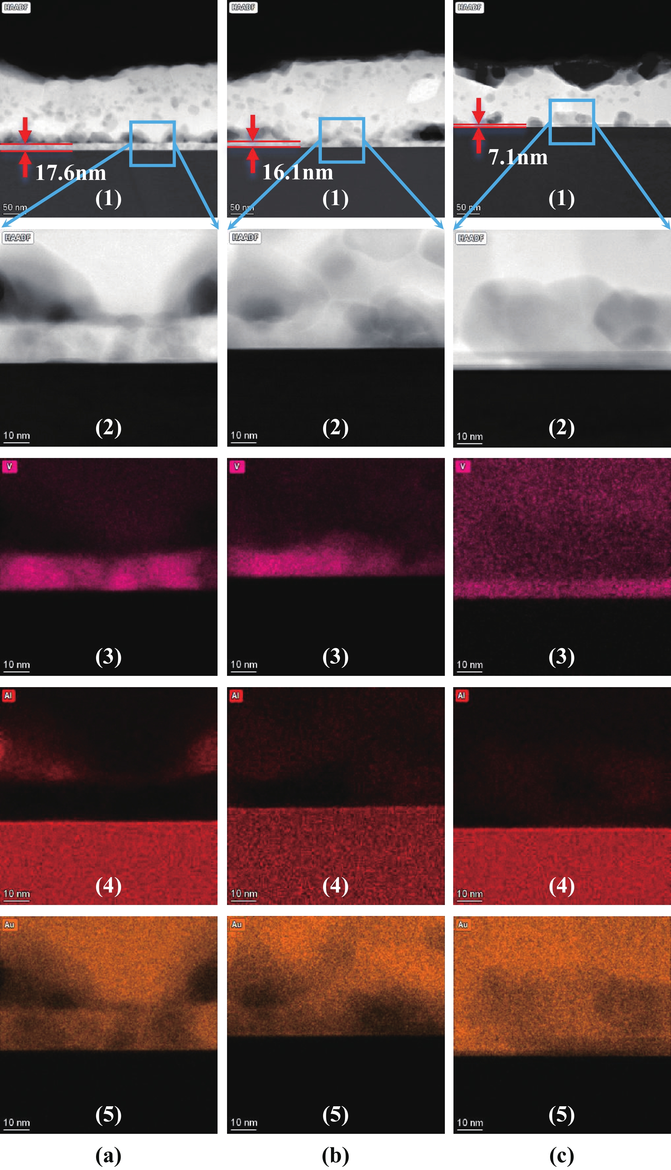
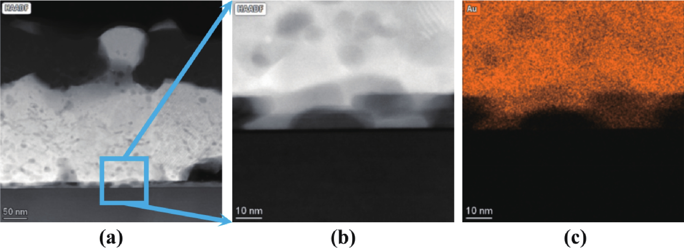
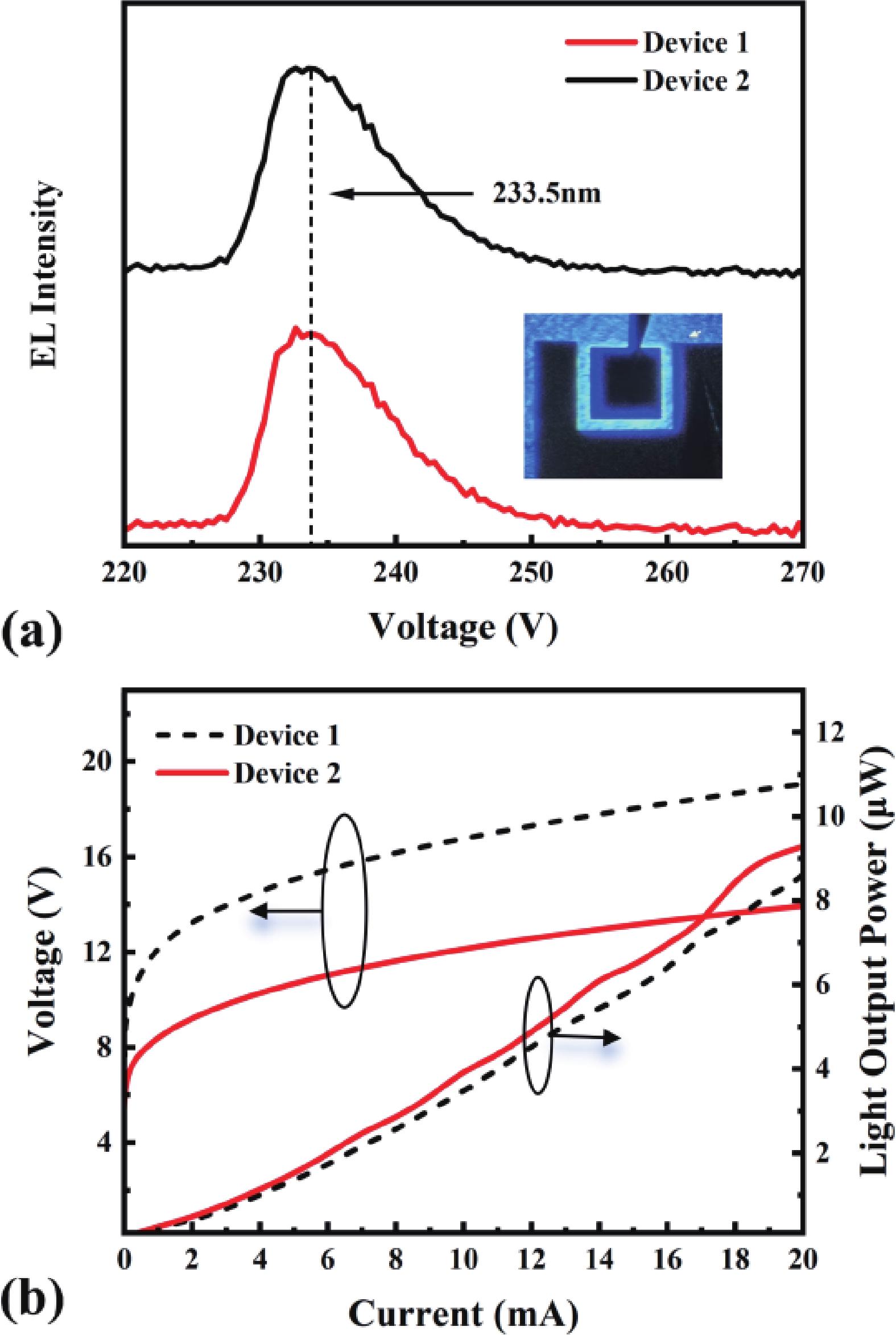
AlGaN-based LEDs with peak wavelength below 240 nm (far-UVC) pose no significant harm to human health, thus highlighting their broader application potential. While, there is a significant Schottky barrier between the n-electrode and Al-rich n-AlGaN, adversely impeding electron injection and resulting in considerable heat generation. Here, we fabricate V-based electrodes of V/Al/Ti/Au on n-AlGaN with Al content over 80% and investigate the relationship between the metal diffusion and contact properties during the high-temperature annealing process. Experiments reveal that decreasing V thickness in the electrode promotes the diffusion of Al towards the surface of n-AlGaN, which facilitates the formation of VN and thus the increase of local electron concentration, resulting in lower specific contact resistivity. Then, increasing the Al thickness inhibits the diffusion of Au to the n-AlGaN surface, suppressing the rise of Schottky barrier. Experimentally, an optimized n-electrode of V(10 nm)/Al(240 nm)/Ti(40 nm)/Au(50 nm) on n-Al0.81Ga0.19N is obtained, realizing an optimal specific contact resistivity of 7.30 × 10⁻⁴ Ω·cm2. Based on the optimal n-electrode preparation scheme for Al-rich n-AlGaN, the work voltage of a far-UVC LED with peak wavelength of 233.5 nm is effectively reduced.
J. Semicond.
2025, 46(9): 092502 doi: 10.1088/1674-4926/25010024
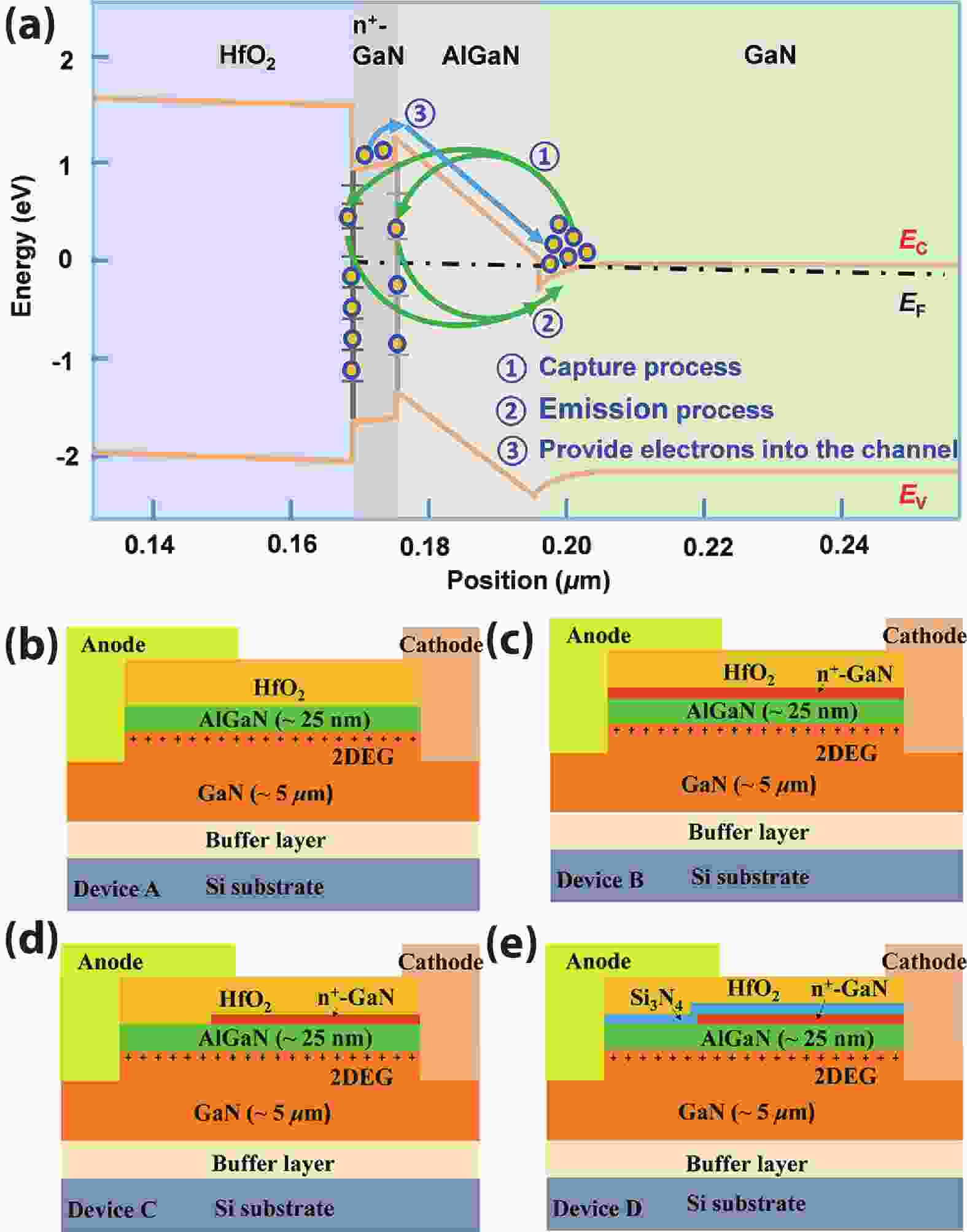
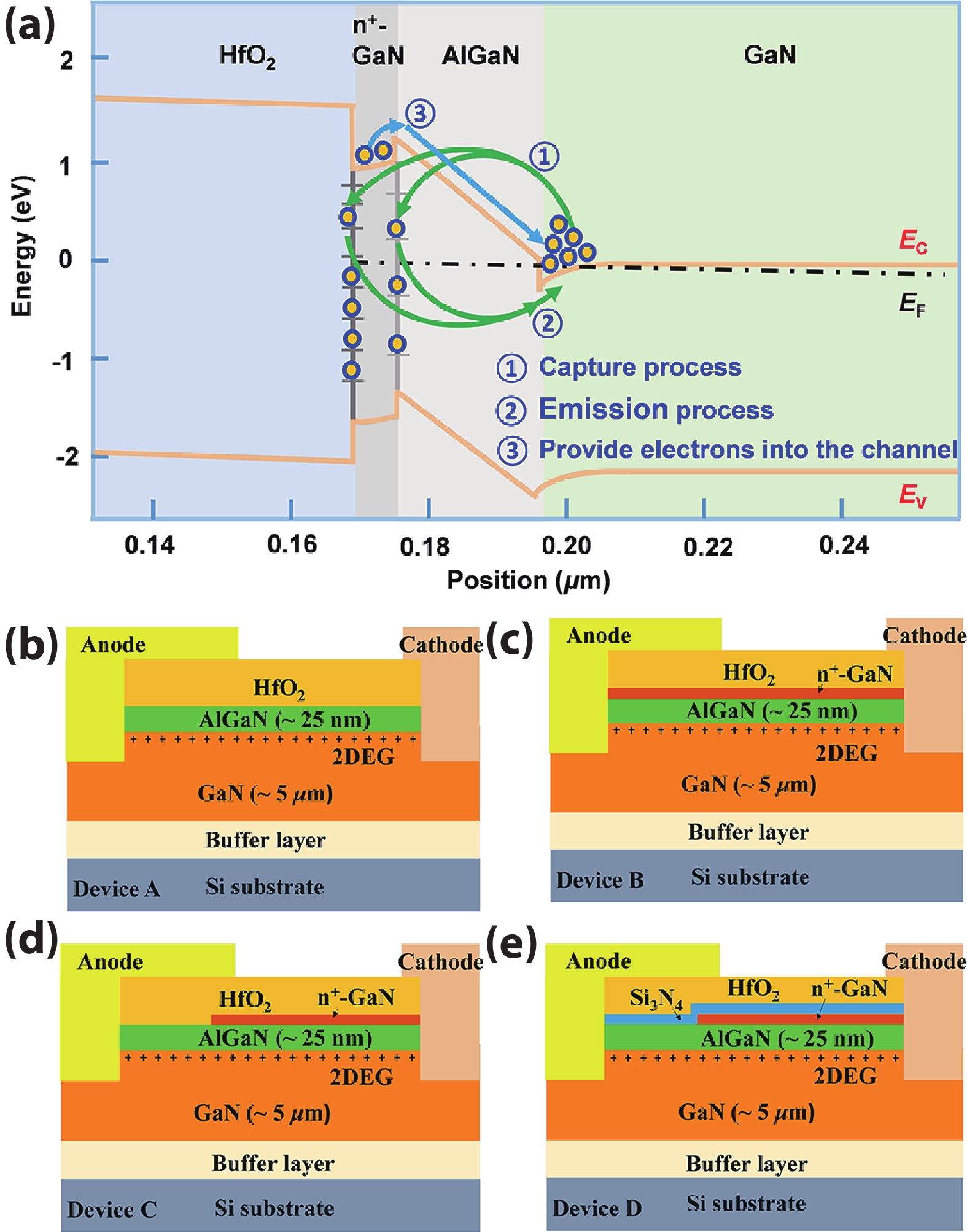
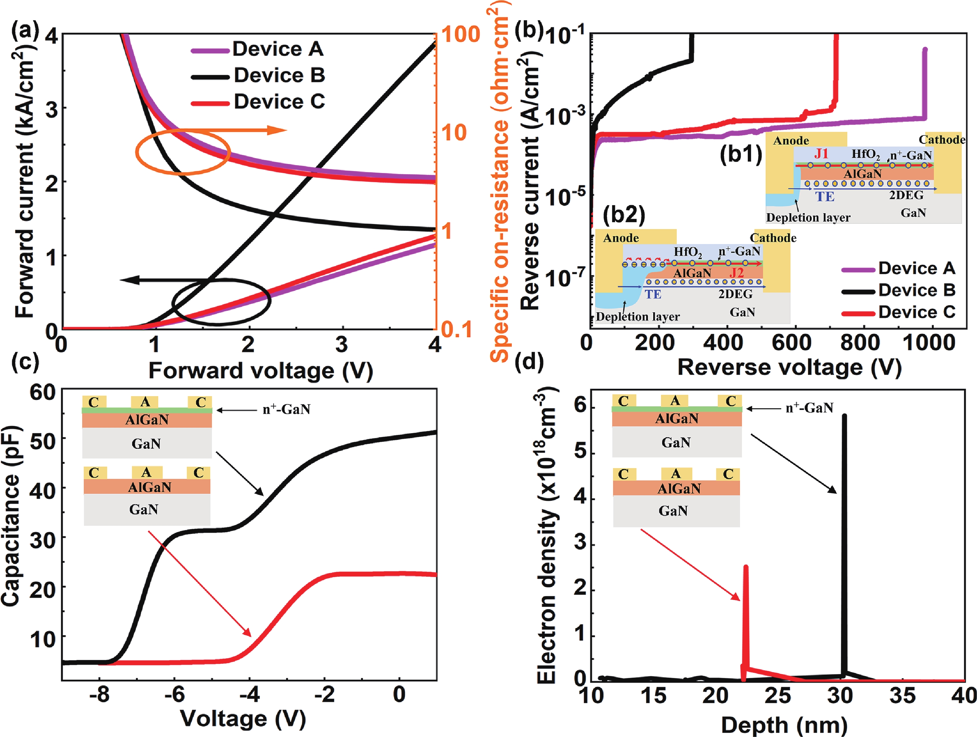
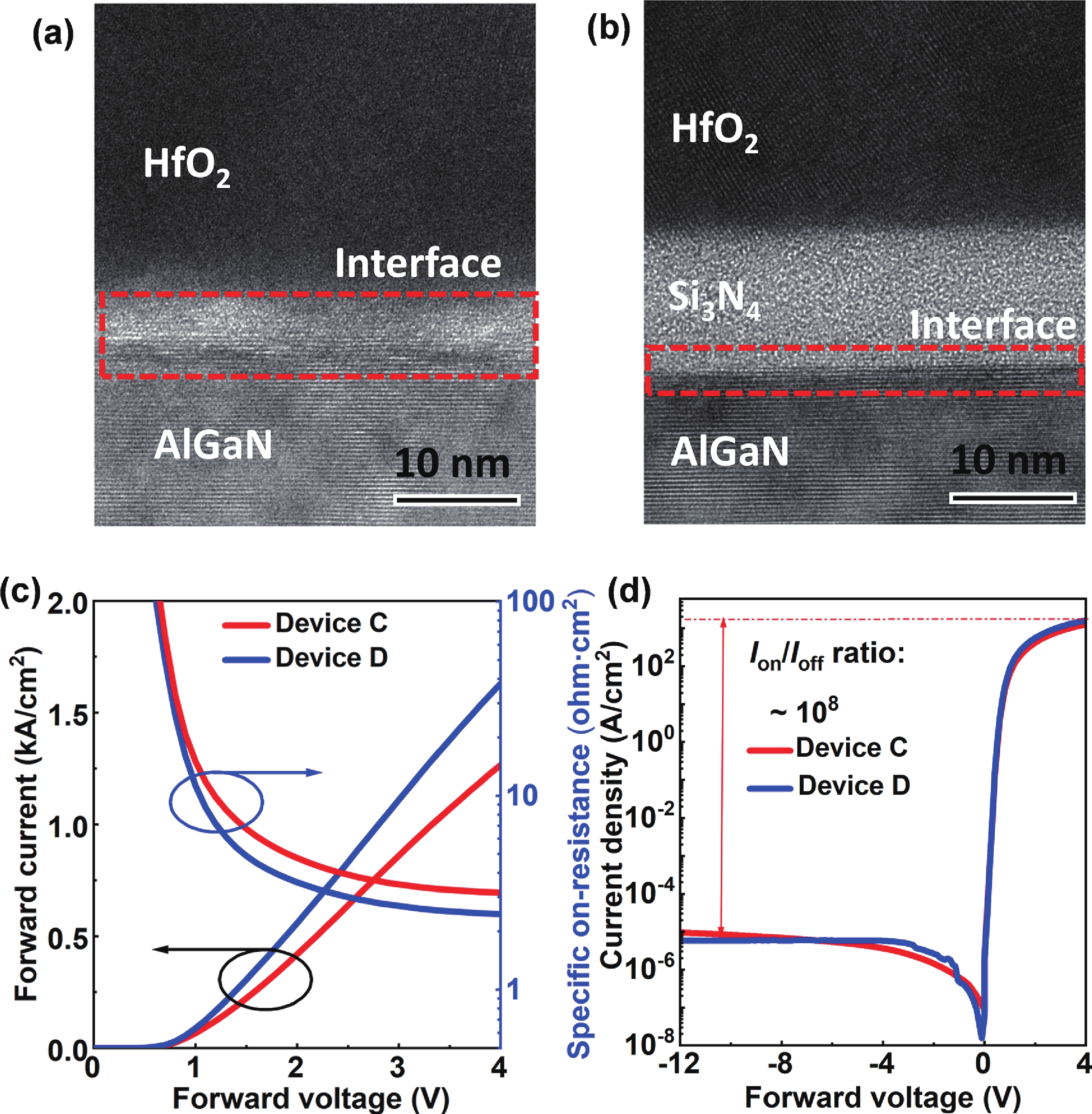
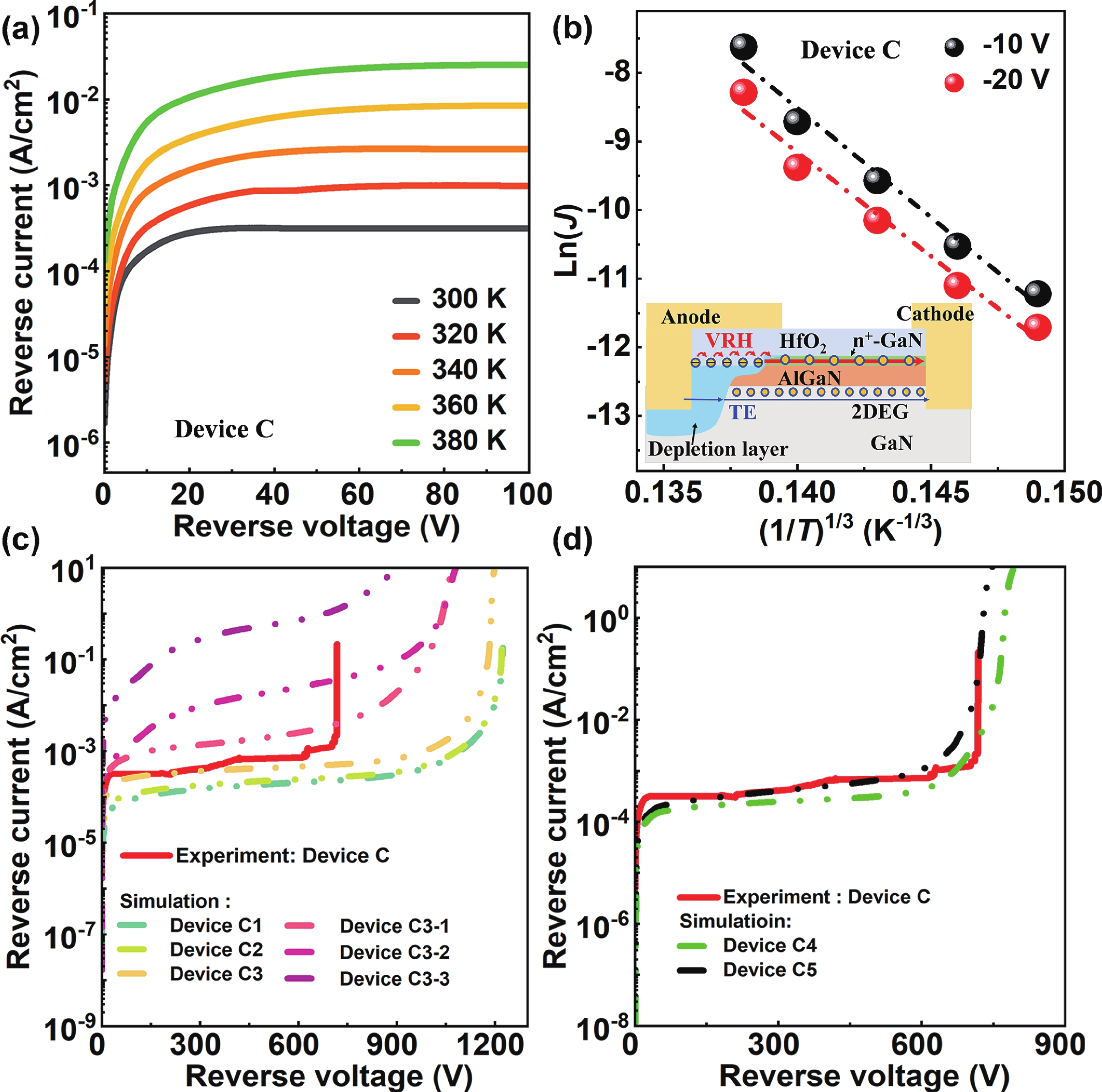
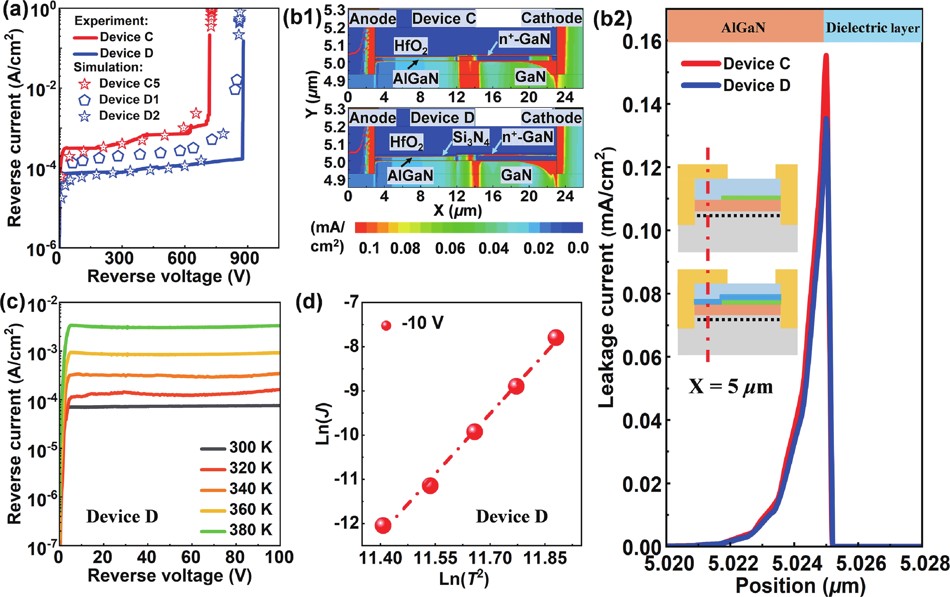
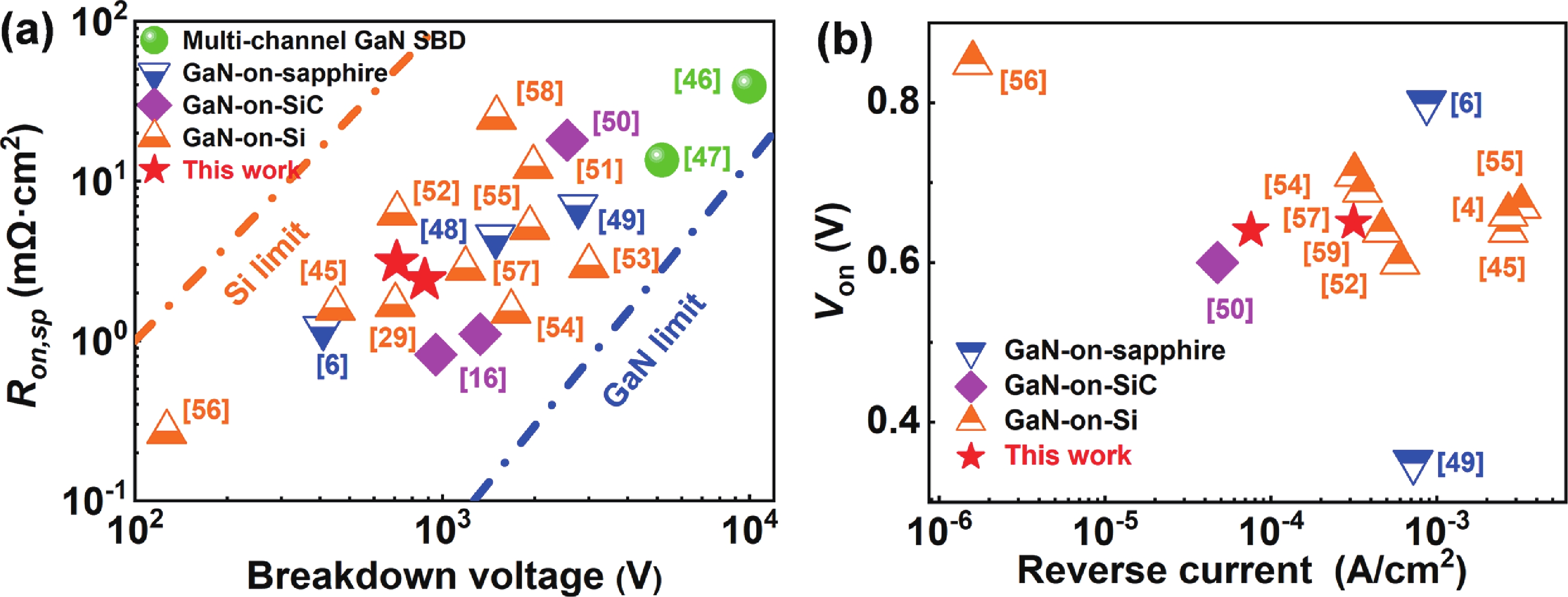
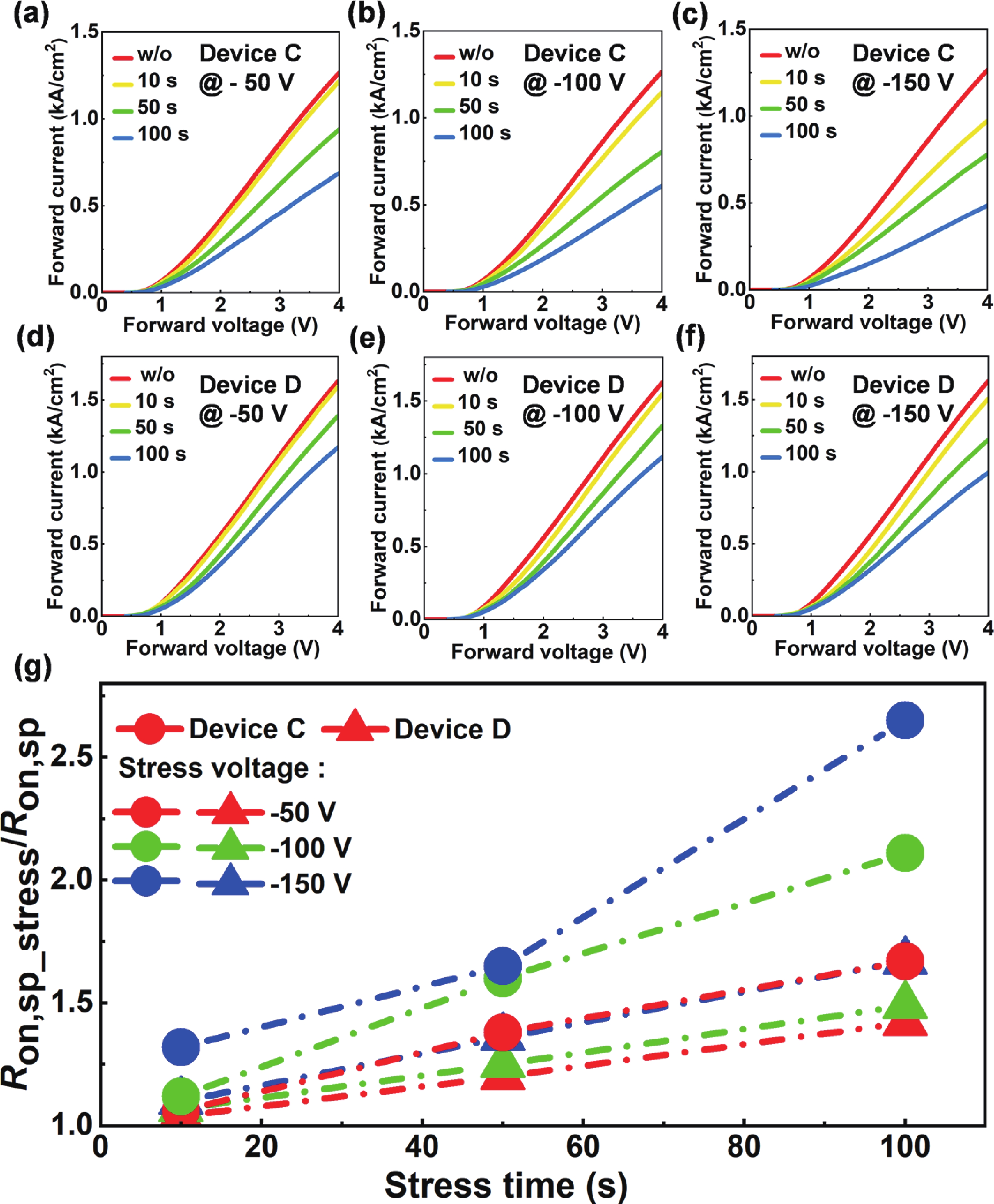
In this work, we design and fabricate AlGaN/GaN-based Schottky barrier diodes (SBDs) on a silicon substrate with a trenched n+-GaN cap layer. With the developed physical models, we find that the n+-GaN cap layer provides more electrons into the AlGaN/GaN channel, which is further confirmed experimentally. When compared with the reference device, this increases the two-dimensional electron gas (2DEG) density by two times and leads to a reduced specific ON-resistance (Ron,sp) of ~2.4 mΩ·cm2. We also adopt the trenched n+-GaN structure such that partial of the n+-GaN is removed by using dry etching process to eliminate the surface electrical conduction when the device is set in the off-state. To suppress the surface defects that are caused by the dry etching process, we also deposit Si3N4 layer prior to the deposition of field plate (FP), and we obtain a reduced leakage current of ~8 × 10⁻⁵ A·cm−2 and breakdown voltage (BV) of 876 V. The Baliga’s figure of merit (BFOM) for the proposed structure is increased to ~319 MW·cm−2. Our investigations also find that the pre-deposited Si3N4 layer helps suppress the electron capture and transport processes, which enables the reduced dynamic Ron,sp.
J. Semicond.
2025, 46(9): 092503 doi: 10.1088/1674-4926/25020014

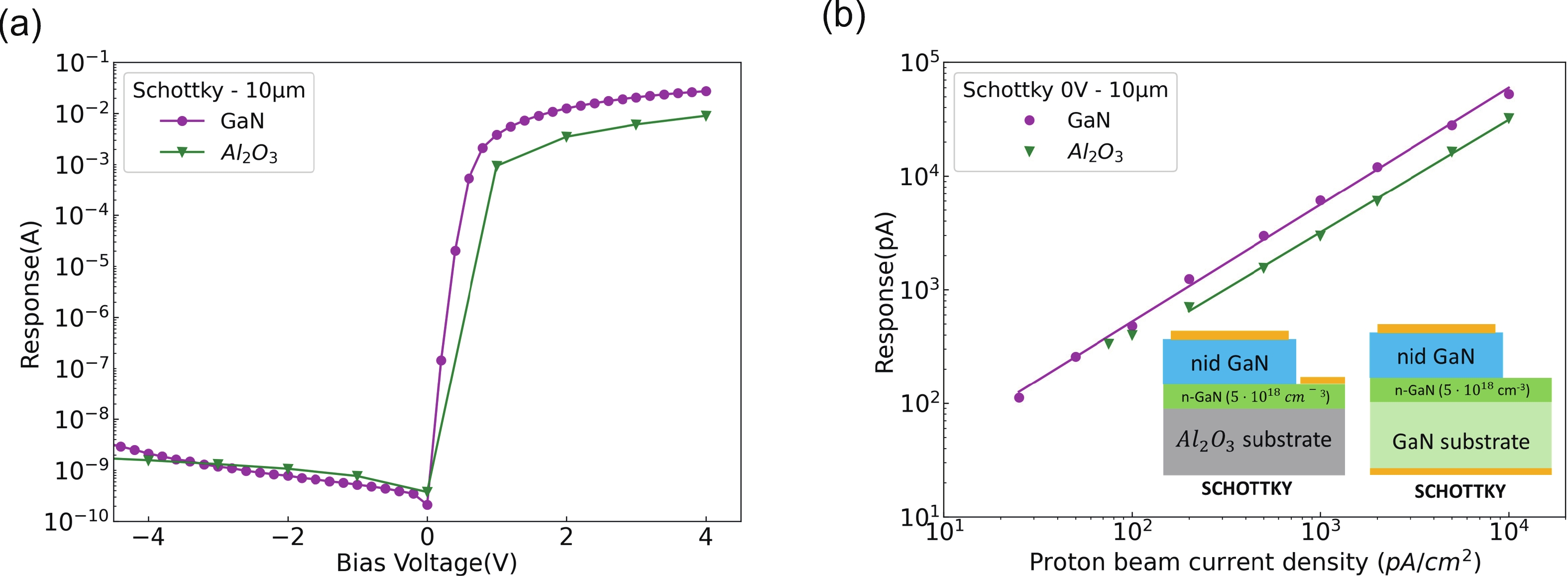
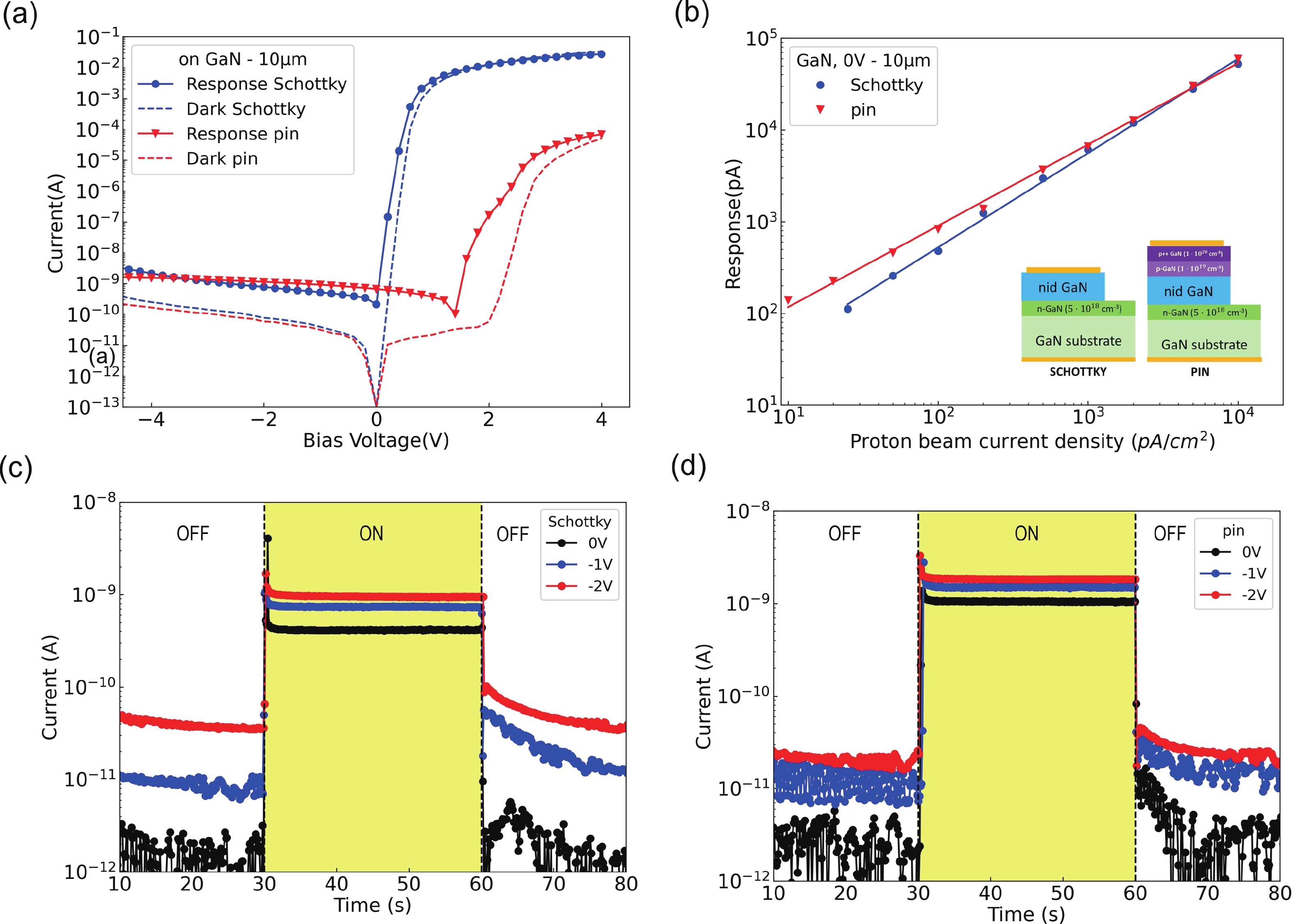
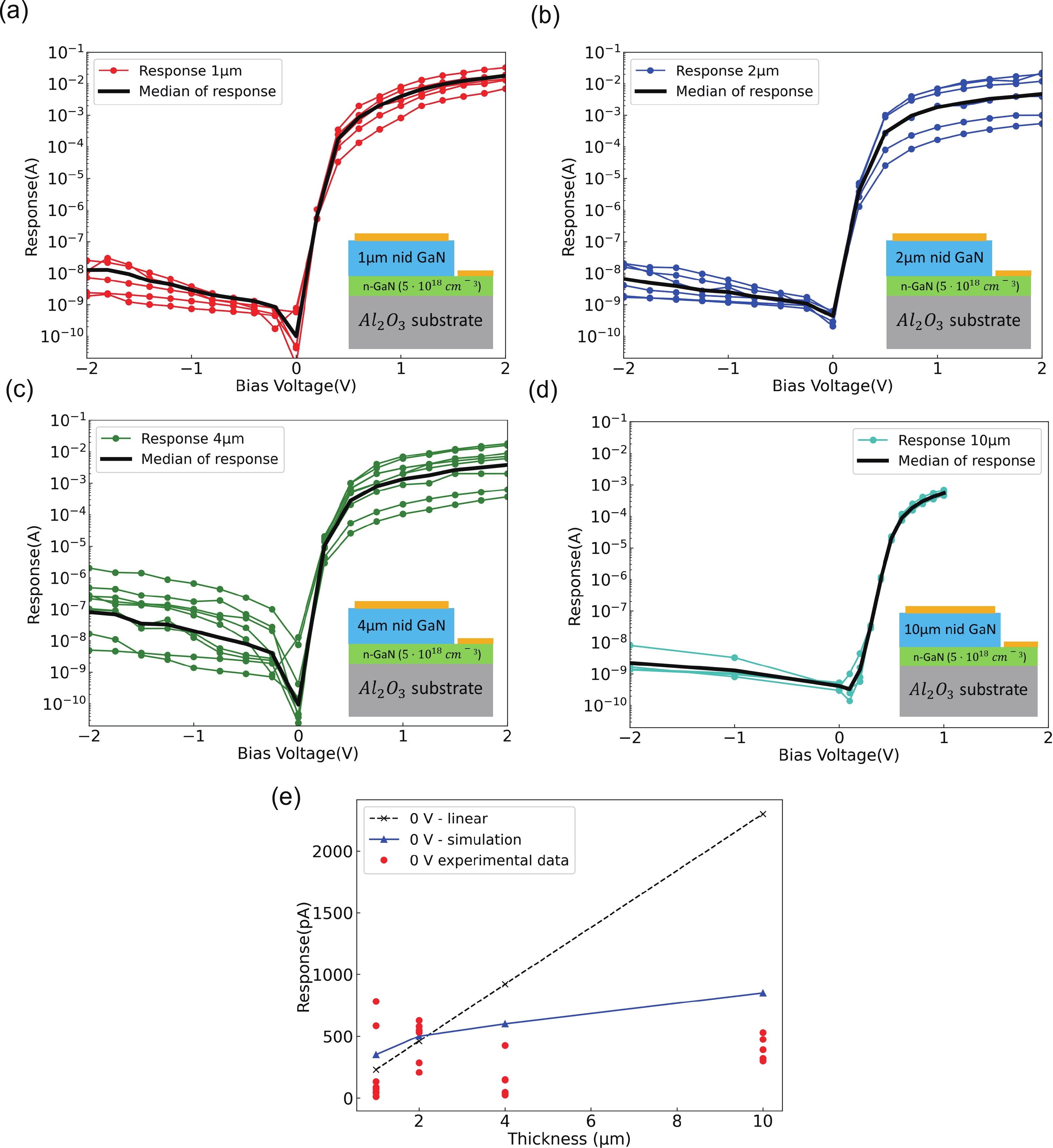
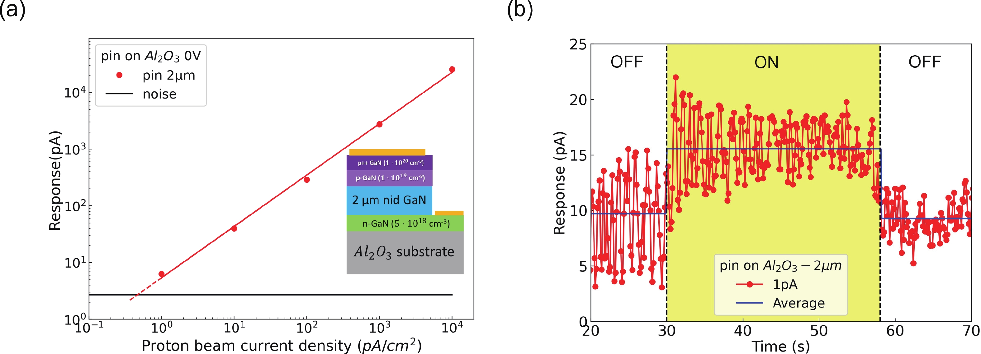
GaN diodes for high energy (64.8 MeV) proton detection were fabricated and investigated. A comparison of the performance of GaN diodes with different structures is presented, with a focus on sapphire and on GaN substrates, Schottky and pin diodes, and different active layer thicknesses. Pin diodes fabricated on a sapphire substrate are the best choice for a GaN proton detector working at 0 V bias. They are sensitive (minimum detectable proton beam <1 pA/cm2), linear as a function of proton current and fast (<1 s). High proton current sensitivity and high spatial resolution of GaN diodes can be exploited in the future for proton imaging of patients in proton therapy.
J. Semicond.
2025, 46(9): 092601 doi: 10.1088/1674-4926/25030009
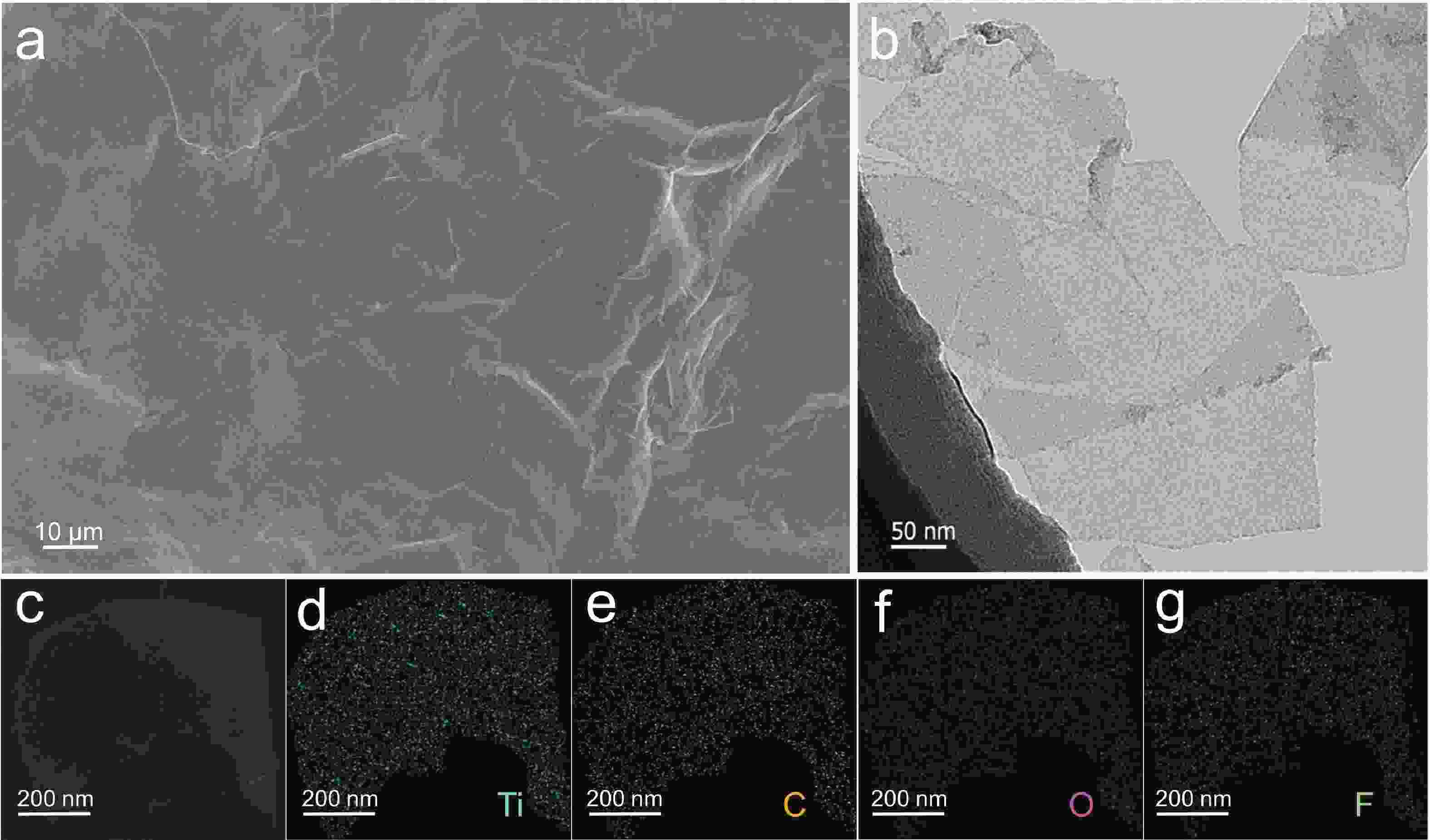
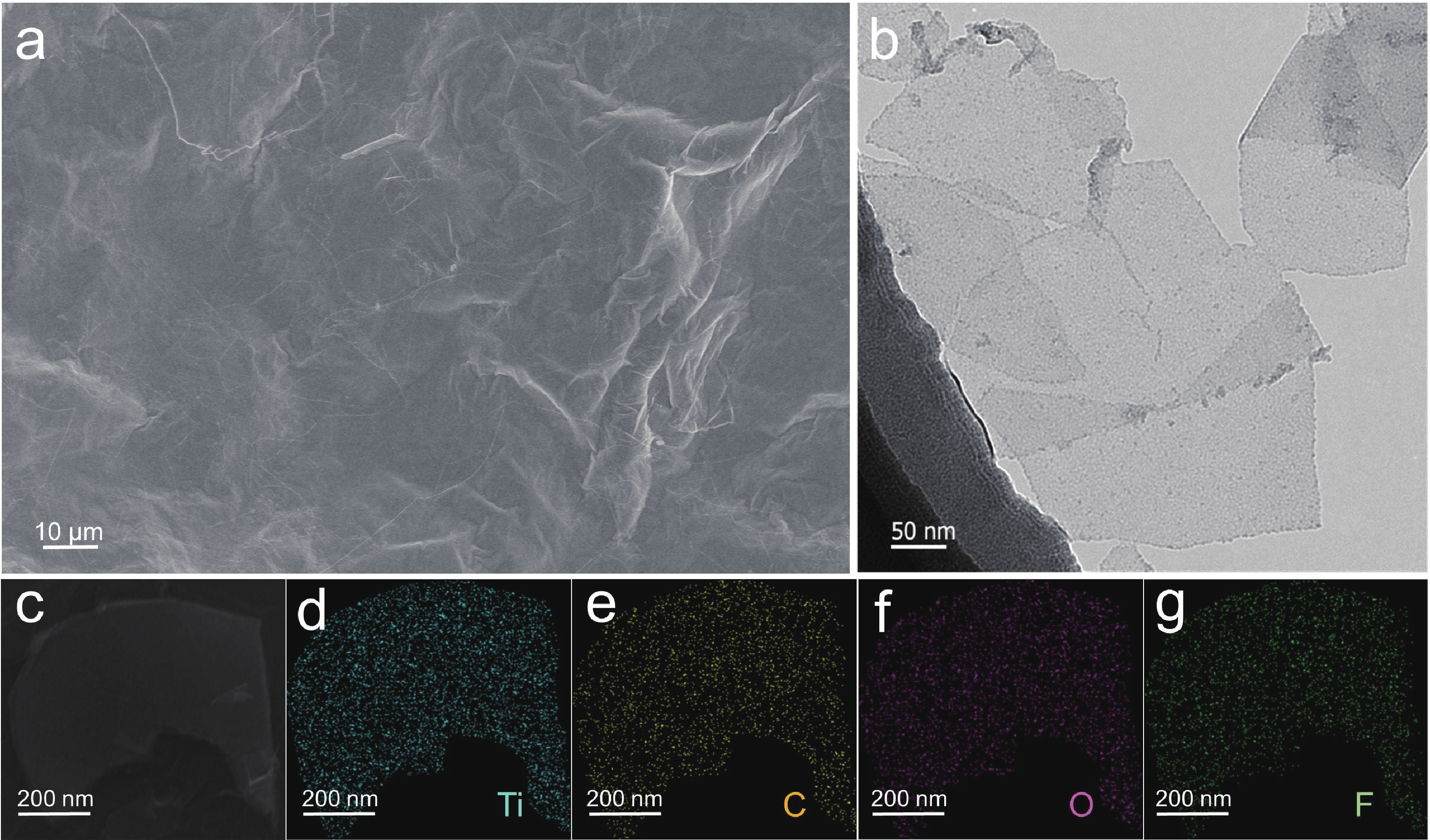
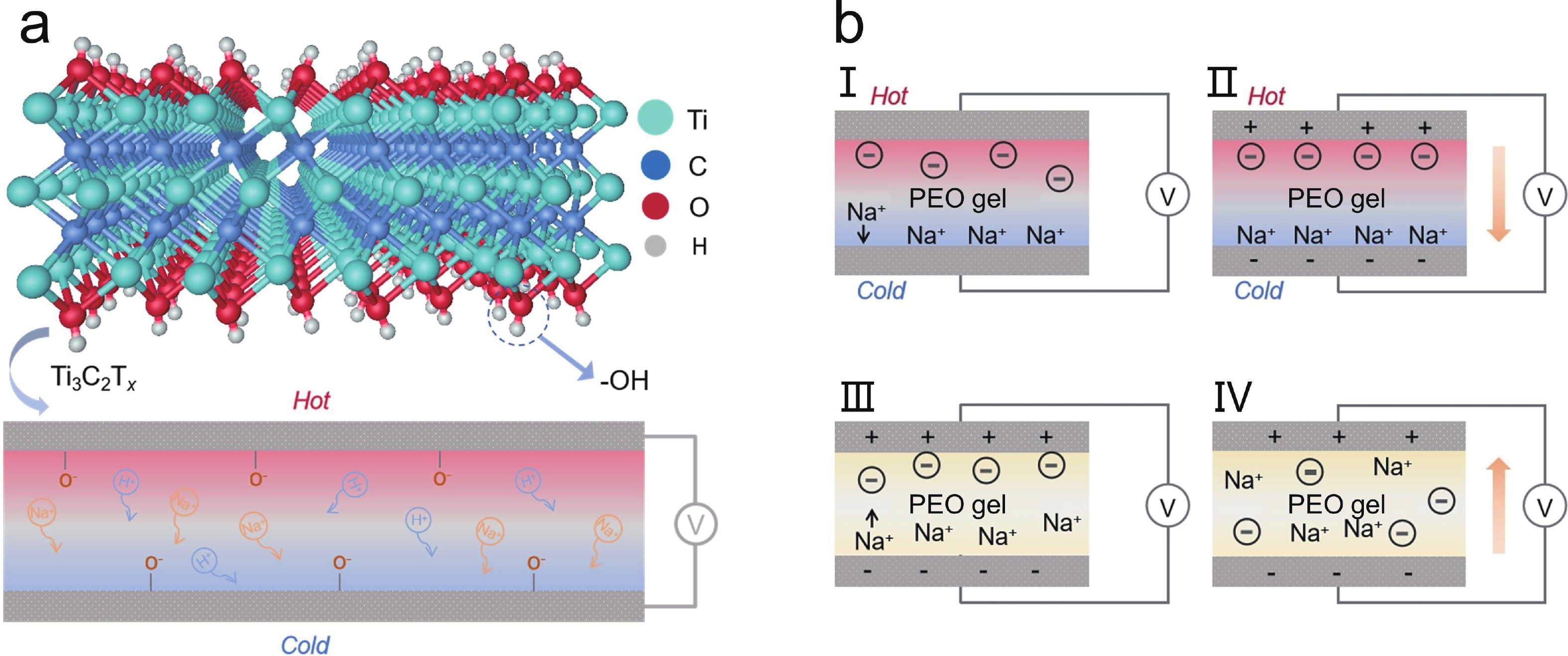
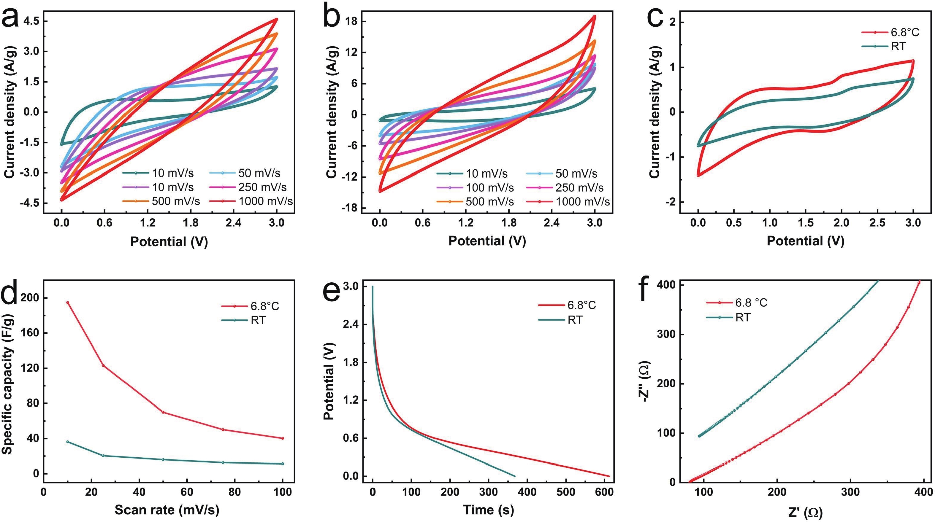
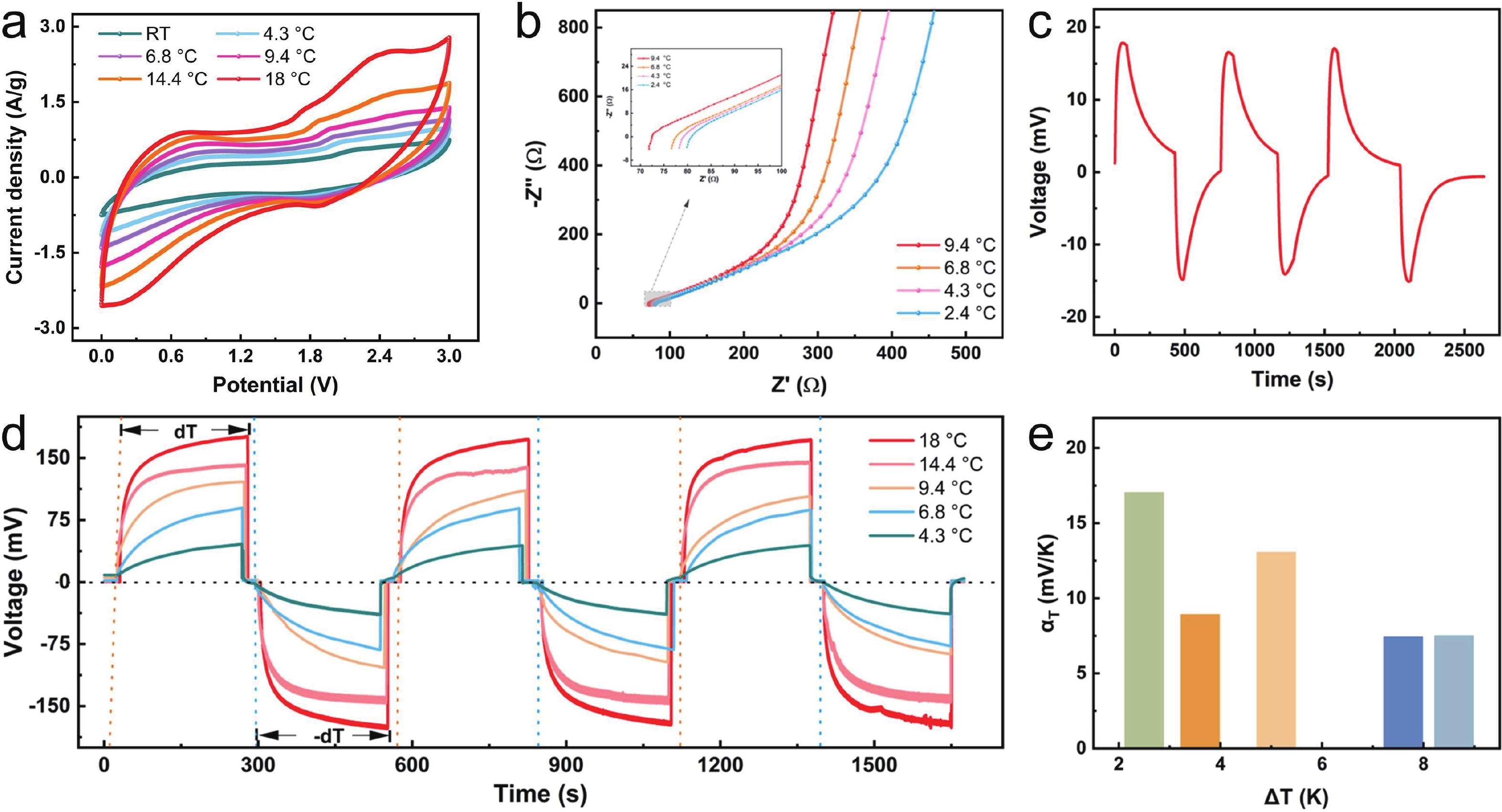
Thermally chargeable supercapacitors (TCSCs) have unique advantages in the collection, conversion, and storage of thermal energy, contributing to the development of new strategies for thermal energy utilization. 2D MXene materials are predicted to be highly promising new thermoelectric materials. Here, we report a self-assembled flexible Ti3C2Tx MXene-based TCSC device, using prepared Ti3C2Tx MXene as the capacitor electrode and a NaClO4/PEO gel as the electrolyte. We also explore the working mechanism of the TCSCs. The fabricated Ti3C2Tx-based TCSCs exhibit an excellent Seebeck coefficient of 11.8 mV∙K−1 on average and maintain good cycling stability under various temperature differences. Demonstrations of multiple practical applications show that Ti3C2Tx MXene-based TCSC devices are excellent candidates for self-powered integrated electronic devices.
J. Semicond.
2025, 46(9): 092602 doi: 10.1088/1674-4926/25010031
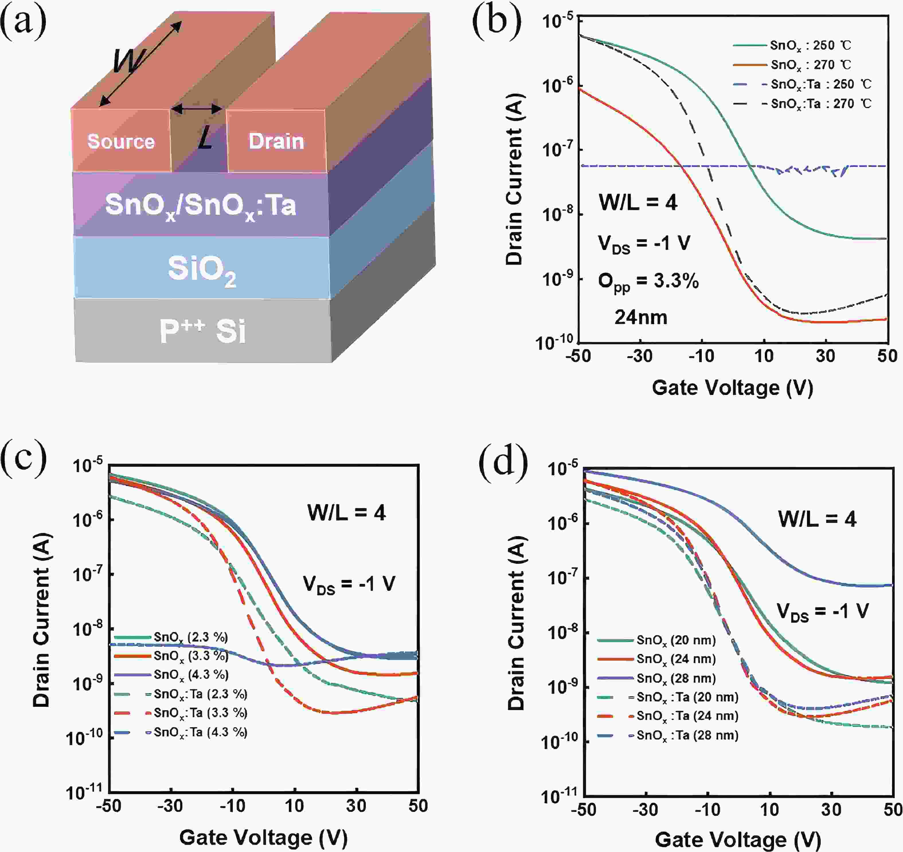
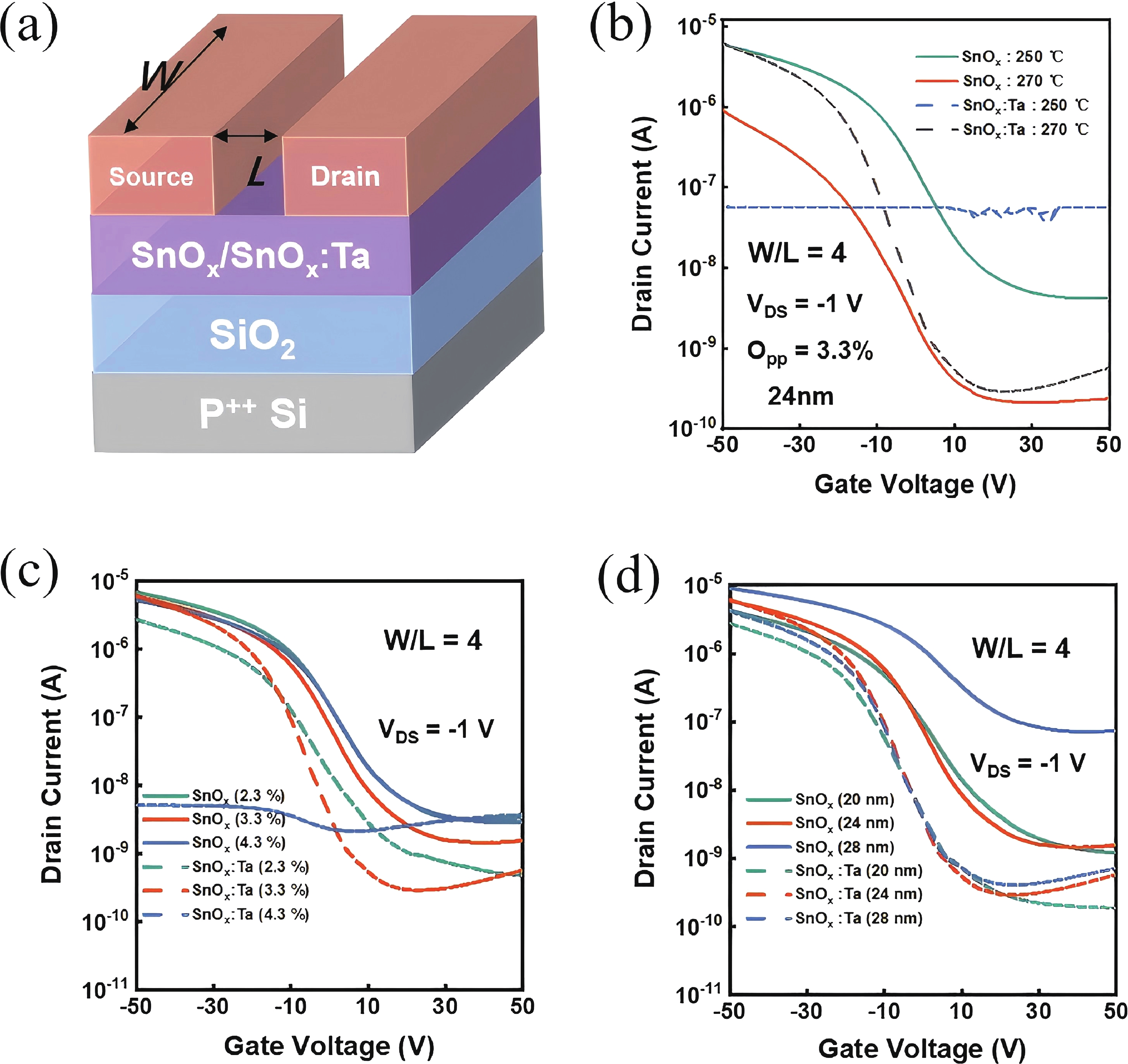
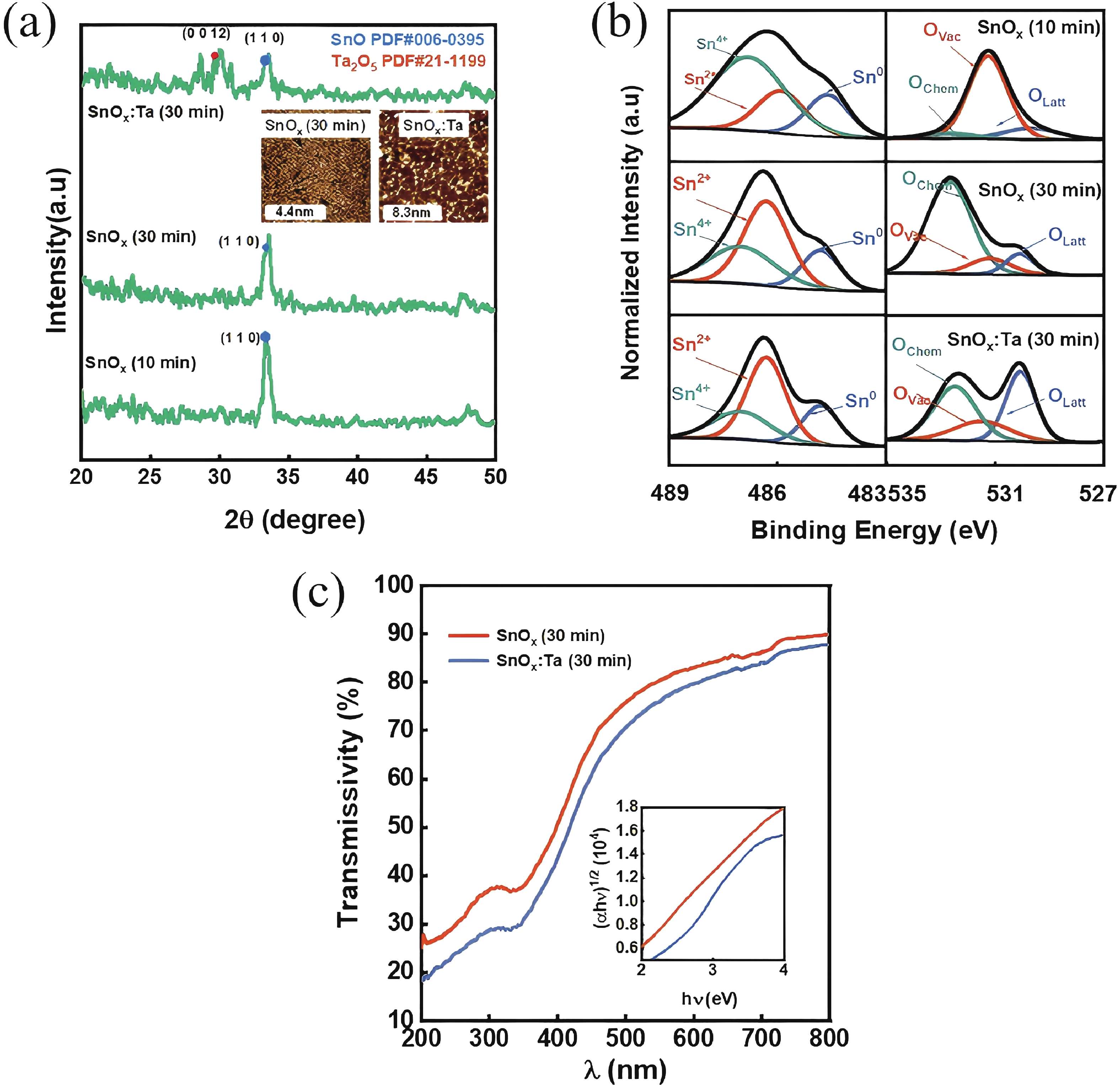
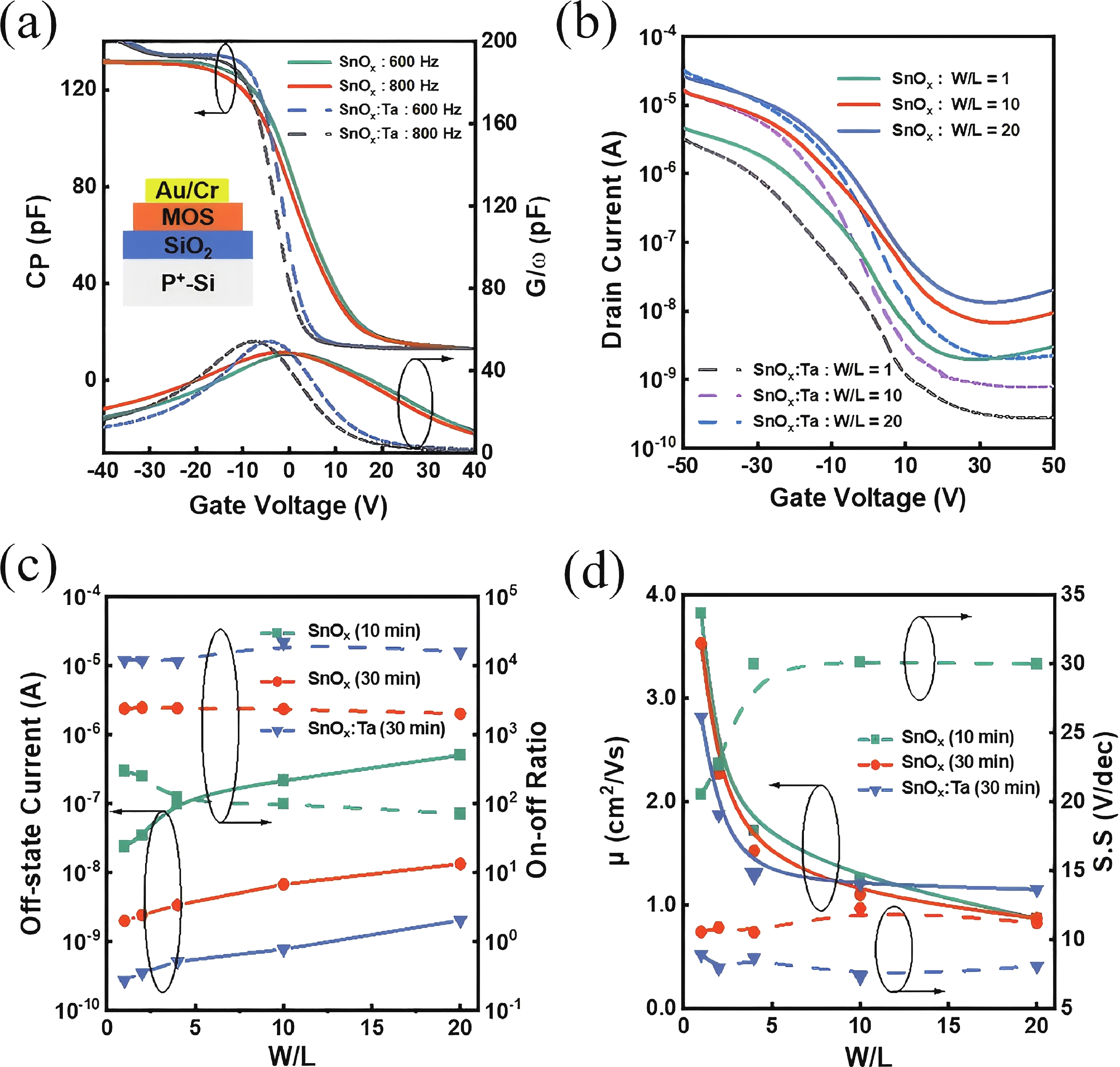
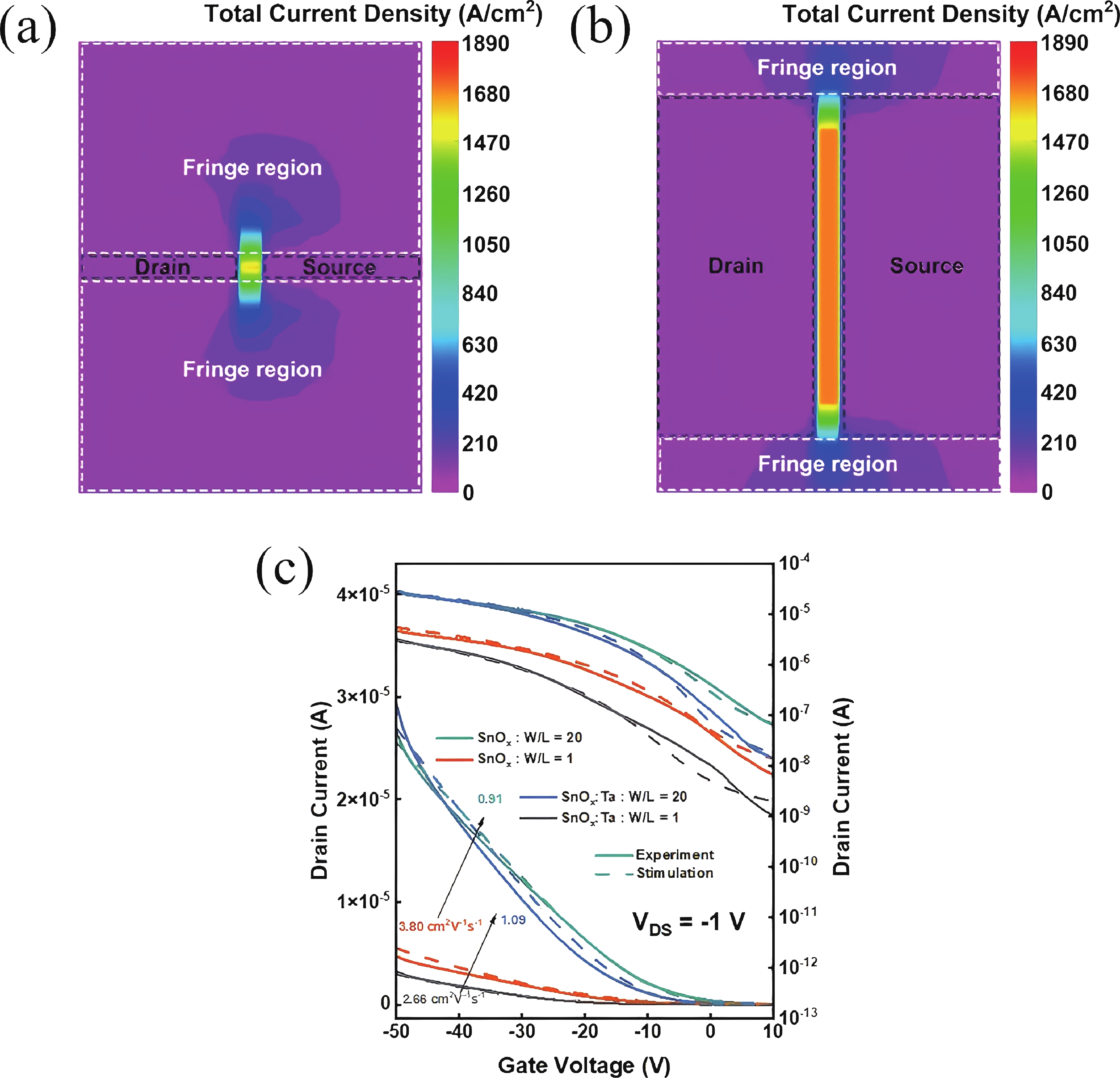
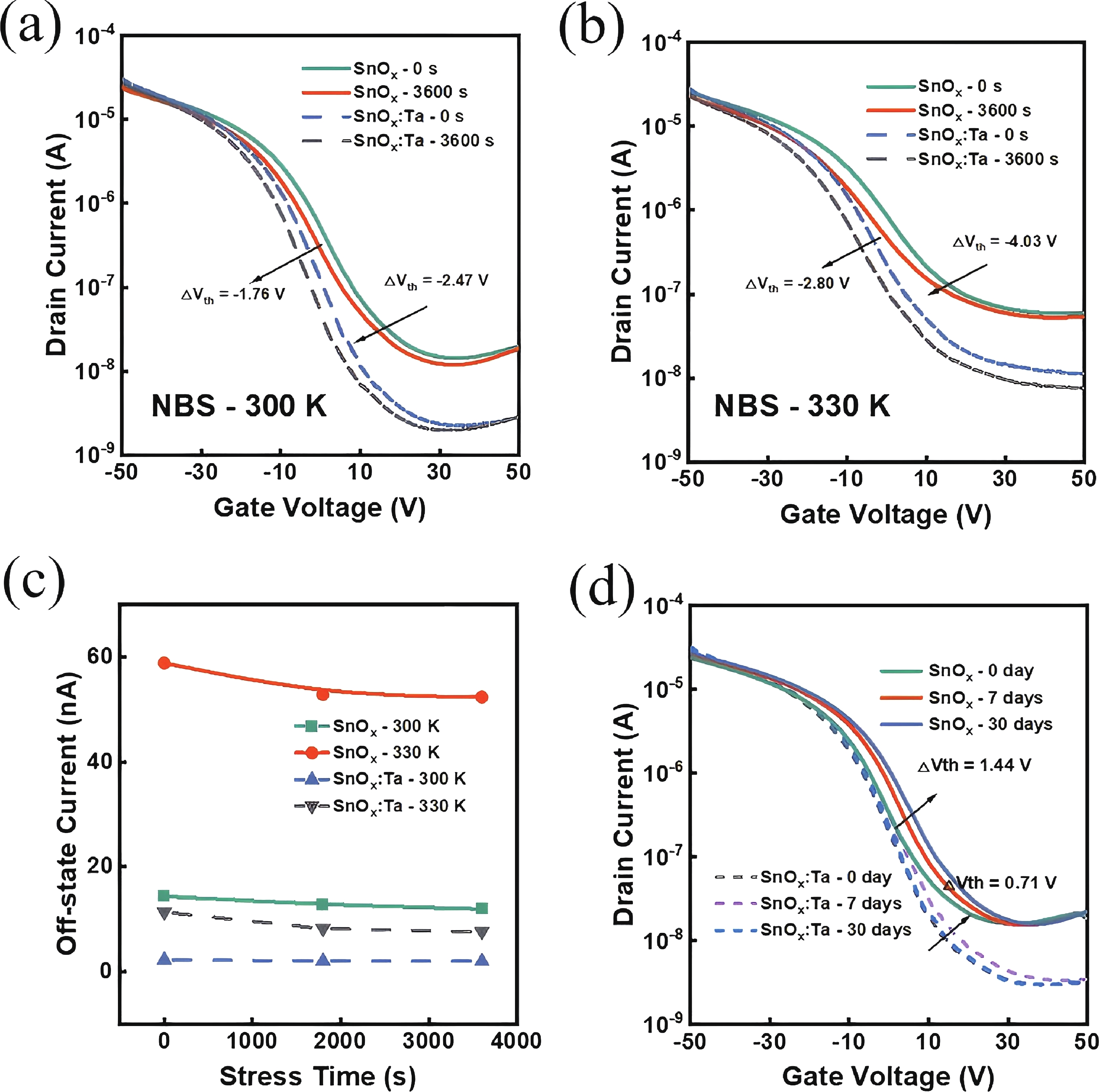
In this work, the incorporation of tantalum (Ta) into p-type metal-oxide (SnOx) semiconductor film is investigated to improve the electrical characteristics and suppress the fringe effect of thin film transistors (TFTs). The Ta-doped SnOx (SnOx:Ta) film is deposited by radio-frequency (RF) magnetron sputtering with a Sn:Ta (3 at.%) target and thermally annealed at 270 °C for 30 min. Here, we observe that the SnOx:Ta film presents increased crystallinity, reduced defect density (3.25 × 1012 cm−2·eV−1), and widened bandgap (1.98 eV), in comparison with the undoped SnOx film. As a result, the SnOx:Ta TFTs exhibit a lower off-state current (Ioff), an improved on/off current ratio (2.17 × 10⁴), a remarkably decreased subthreshold swing (SS) by 41%, and enhanced device stability. Additionally, by introducing Ta dopants, the fringe effect as well as the impact of channel width-to-length ratio (W/L) on electrical performances of the p-type oxide TFTs can be effectively suppressed. These results shall contribute to further exploration and development of p-type SnOx TFTs.