J. Semicond. >  Just Accepted

ARTICLES

AlGaN/GaN-based SBDs grown on silicon substrates with trenched n+-GaN cap layer and local passivation layer to improve BFOM and dynamic properties

Zhizhong Wang1, Jingting He2, Fuping Huang2, Xuchen Gao1, Kangkai Tian2, Chunshuang Chu2, Yonghui Zhang1, Shuting Cai2, Xiaojuan Sun3, Dabing Li3, Xiao Wei Sun4 and Zi-Hui Zhang1, 2,

+ Author Affiliations

 Corresponding author: Zi-Hui Zhang, zh.zhang@hebut.edu.cn

DOI: 10.1088/1674-4926/25010024CSTR: 32376.14.1674-4926.25010024

PDF

Turn off MathJax

Abstract: In this work, we design and fabricate AlGaN/GaN-based Schottky barrier diodes (SBDs) on a silicon substrate with a trenched n+-GaN cap layer. With the developed physical models, we find that the n+-GaN cap layer provides more electrons into the AlGaN/GaN channel, which is further confirmed experimentally. When compared with the reference device, this increases the two-dimensional electron gas (2DEG) density by two times and leads to a reduced specific ON-resistance (Ron,sp)of ~2.4 mΩ·cm2. We also adopt the trenched n+-GaN structure such that partial of the n+-GaN is removed by using dry etching process to eliminate the surface electrical conduction when the device is set in the off-state. To suppress the surface defects that are caused by the dry etching process, we also deposit Si3N4 layer prior to the deposition of field plate (FP), and we obtain a reduced leakage current of ~8 × 10⁻⁵ A·cm−2 and breakdown voltage (BV) of 876 V. The Baliga’s figure of merit (BFOM) for the proposed structure is increased to ~319 MW·cm−2. Our investigations also find that the pre-deposited Si3N4 layer helps suppress the electron capture and transport processes, which enables the reduced dynamic Ron,sp.

Key words: AlGaN/GaN-based Schottky barrier diodes (SBDs)n+-GaN cap layerSi3N4 protective layer


[1]
Islam N, Mohamed M F P, Khan M F A J, et al. Reliability, applications and challenges of GaN HEMT technology for modern power devices: A review. Crystals, 2022, 12(11), 1581 doi: 10.3390/cryst12111581
[2]
Mounika B, Ajayan J, Bhattacharya S, et al. Recent developments in materials, architectures and processing of AlGaN/GaN HEMTs for future RF and power electronic applications: A critical review. Micro Nanostruct, 2022, 168, 207317 doi: 10.1016/j.micrna.2022.207317
[3]
Zhang T, Wang Y, Zhang Y N, et al. Comprehensive annealing effects on AlGaN/GaN Schottky barrier diodes with different work-function metals. IEEE Trans Electron Devices, 2021, 68(6), 2661 doi: 10.1109/TED.2021.3074896
[4]
Zhou Q, Jin Y, Shi Y Y, et al. High reverse blocking and low onset voltage AlGaN/GaN-on-Si lateral power diode with MIS-gated hybrid anode. IEEE Electron Device Lett, 2015, 36(7), 660 doi: 10.1109/LED.2015.2432171
[5]
Rajagopal Reddy V, Janardhanam V, Ju J W, et al. Electronic parameters and carrier transport mechanism of high-barrier Se Schottky contacts to n-type GaN. Solid State Commun, 2014, 179, 34 doi: 10.1016/j.ssc.2013.11.011
[6]
Yang X X, Cheng Z, Yu Z G, et al. The influence of anode trench geometries on electrical properties of AlGaN/GaN Schottky barrier diodes. Electronics, 2020, 9(2), 282 doi: 10.3390/electronics9020282
[7]
Wang T F, Zong Y, Nela L, et al. Enhancement-mode multi-channel AlGaN/GaN transistors with LiNiO junction tri-gate. IEEE Electron Device Lett, 2022, 43(9), 1523 doi: 10.1109/LED.2022.3189635
[8]
Nela L, Xiao M, Zhang Y H, et al. A perspective on multi-channel technology for the next-generation of GaN power devices. Appl Phys Lett, 2022, 120(19), 190501 doi: 10.1063/5.0086978
[9]
Li C K, Wu Y R. Study on the current spreading effect and light extraction enhancement of vertical GaN/InGaN LEDs. IEEE Trans Electron Devices, 2012, 59(2), 400 doi: 10.1109/TED.2011.2176132
[10]
Ibbetson J P, Fini P T, Ness K D, et al. Polarization effects, surface states, and the source of electrons in AlGaN/GaN heterostructure field effect transistors. Appl Phys Lett, 2000, 77(2), 250 doi: 10.1063/1.126940
[11]
Lee J H, Im K S, Lee J H. Effect of In-situ silicon carbon nitride (SiCN) cap layer on performances of AlGaN/GaN MISHFETs. IEEE J Electron Devices Soc, 2021, 9, 728 doi: 10.1109/JEDS.2021.3100760
[12]
Hsu L, Jones R E, Li S X, et al. Electron mobility in InN and III-N alloys. J Appl Phys, 2007, 102(7), 073705 doi: 10.1063/1.2785005
[13]
Wang J X, Yang S Y, Wang J, et al. Electron mobility limited by surface and interface roughness scattering in Al xGa1− xN/GaN quantum wells. Chin Phys B, 2013, 22(7), 077305 doi: 10.1088/1674-1056/22/7/077305
[14]
Ko T S, Lin D Y, Lin C F, et al. High-temperature carrier density and mobility enhancements in AlGaN/GaN HEMT using AlN spacer layer. J Cryst Growth, 2017, 464, 175 doi: 10.1016/j.jcrysgro.2016.12.023
[15]
Liu Z H, Ng G I, Zhou H, et al. Reduced surface leakage current and trapping effects in AlGaN/GaN high electron mobility transistors on silicon with SiN/Al2O3 passivation. Appl Phys Lett, 2011, 98(11), 113506 doi: 10.1063/1.3567927
[16]
Rahman M W, Chandrasekar H, Razzak T, et al. Hybrid BaTiO3/SiNx/AlGaN/GaN lateral Schottky barrier diodes with low turn-on and high breakdown performance. Appl Phys Lett, 2021, 119(1), 013504 doi: 10.1063/5.0055946
[17]
Huang F P, Wang Z Z, Chu C S, et al. MIS-based GaN Schottky barrier diodes: Interfacial conditions on the reverse and forward properties. IEEE Trans Electron Devices, 2022, 69(10), 5522 doi: 10.1109/TED.2022.3201831
[18]
Gao X C, He F, Huang F P, et al. Investigation into the impact of bulk defects in the drift layer on the electrical properties of GaN-based trench Schottky barrier diodes. Jpn J Appl Phys, 2024, 63(5), 054003 doi: 10.35848/1347-4065/ad40eb
[19]
Wong M S, Lee C M, Myers D J, et al. Size-independent peak efficiency of III-nitride micro-light-emitting-diodes using chemical treatment and sidewall passivation. Appl Phys Express, 2019, 12(9), 097004 doi: 10.7567/1882-0786/ab3949
[20]
Wang H Y, Mao W, Yang C, et al. Lateral AlGaN/GaN Schottky barrier diode with arrayed p-GaN islands termination. IEEE Trans Electron Devices, 2021, 68(12), 6046 doi: 10.1109/TED.2021.3118326
[21]
Xiao M, Du Z H, Xie J Q, et al. Lateral p-GaN/2DEG junction diodes by selective-area p-GaN trench-filling-regrowth in AlGaN/GaN. Appl Phys Lett, 2020, 116(5), 053503 doi: 10.1063/1.5139906
[22]
Dang K, Zhang J C, Zhou H, et al. Lateral GaN Schottky barrier diode for wireless high-power transfer application with high RF/DC conversion efficiency: From circuit construction and device technologies to system demonstration. IEEE Trans Ind Electron, 2020, 67(8), 6597 doi: 10.1109/TIE.2019.2939968
[23]
Huang F P, Chu C S, Wang Z Z, et al. 1.43 kV GaN-based MIS Schottky barrier diodes. J Phys D: Appl Phys, 2024, 57(18), 185102 doi: 10.1088/1361-6463/ad256c
[24]
Letts E, Hashimoto T, Ikari M, et al. Development of GaN wafers for solid-state lighting via the ammonothermal method. J Cryst Growth, 2012, 350(1), 66 doi: 10.1016/j.jcrysgro.2011.12.024
[25]
Wang B F, Liu L, Tian G, et al. Studying the effect of temperature and pressure on GaN crystals via the Na-flux method. CrystEngComm, 2024, 26(24), 3176 doi: 10.1039/D4CE00314D
[26]
Yang S, Han S W, Sheng K, et al. Dynamic on-resistance in GaN power devices: Mechanisms, characterizations, and modeling. IEEE J Emerg Sel Top Power Electron, 2019, 7(3), 1425 doi: 10.1109/JESTPE.2019.2925117
[27]
Zhong Y Z, Zhang J W, Wu S, et al. A review on the GaN-on-Si power electronic devices. Fundam Res, 2022, 2(3), 462 doi: 10.1016/j.fmre.2021.11.028
[28]
Li H, Bai Z Y, Yang L. Investigation of double RESURF P-GaN gate AlGaN/GaN heterostructure field-effect transistors with partial N-GaN channels. J Electron Mater, 2024, 53(5), 2562 doi: 10.1007/s11664-024-10987-0
[29]
Lei J C, Wei J, Tang G F, et al. 650-V double-channel lateral Schottky barrier diode with dual-recess gated anode. IEEE Electron Device Lett, 2018, 39(2), 260 doi: 10.1109/LED.2017.2783908
[30]
Xu J Y, Liu X, Xie B, et al. Correlation between reverse leakage current and electric field spreading in GaN vertical SBD with high-energy ion implanted guard rings. IEEE Trans Electron Devices, 2023, 70(4), 1745 doi: 10.1109/TED.2023.3241260
[31]
Chen H, Wang H Y, Sheng K. Vertical β-Ga2O3 Schottky barrier diodes with field plate assisted negative beveled termination and positive beveled termination. IEEE Electron Device Lett, 2023, 44(1), 21 doi: 10.1109/LED.2022.3222878
[32]
Wang Z Z, Huang F P, Chu C S, et al. 2.5 kV/1.95 GW/cm2 AlGaN/GaN-based lateral Schottky barrier diodes with a high-k field plate to reduce reverse current. IEEE Trans Electron Devices, 2024, 71(6), 3811 doi: 10.1109/TED.2024.3388377
[33]
Nguyen X S, Goh X L, Zhang L, et al. Deep level traps in GaN LEDs grown by metal organic vapour phase epitaxy on an 8 inch Si(111) substrate. Jpn J Appl Phys, 2016, 55(6), 060306 doi: 10.7567/JJAP.55.060306
[34]
Cho H K, Kim C S, Hong C H. Electron capture behaviors of deep level traps in unintentionally doped and intentionally doped n-type GaN. J Appl Phys, 2003, 94(3), 1485 doi: 10.1063/1.1586981
[35]
Soh C B, Chua S J, Lim H F, et al. Identification of deep levels in GaN associated with dislocations. J Phys Condens Matter, 2004, 16(34), 6305 doi: 10.1088/0953-8984/16/34/027
[36]
Lee I H, Polyakov A Y, Smirnov N B, et al. Spatial location of the Ec-0.6 eV electron trap in AlGaN/GaN heterojunctions. J Vac Sci Technol B, 2014, 32(5), 050602 doi: 10.1116/1.4895840
[37]
Cao L N, Wang J S, Harden G, et al. Experimental characterization of impact ionization coefficients for electrons and holes in GaN grown on bulk GaN substrates. Appl Phys Lett, 2018, 112(26), 262103 doi: 10.1063/1.5031785
[38]
Ambacher O, Smart J, Shealy J R, et al. Two-dimensional electron gases induced by spontaneous and piezoelectric polarization charges in N- and Ga-face AlGaN/GaN heterostructures. J Appl Phys, 1999, 85(6), 3222 doi: 10.1063/1.369664
[39]
Huang F P, Chu C S, Jia X Y, et al. Simulation study for GaN-based hybrid trench MOS barrier Schottky diode with an embedded p-type NiO termination: Increased forward current density and enhanced breakdown voltage. Jpn J Appl Phys, 2022, 61(1), 014002 doi: 10.35848/1347-4065/ac40cf
[40]
Tokuda Y. (invited) DLTS studies of defects in n-GaN. ECS Trans, 2016, 75(4), 39 doi: 10.1149/07504.0039ecst
[41]
Faraz S M, Ashraf H, Imran Arshad M, et al. Interface state density of free-standing GaN Schottky diodes. Semicond Sci Technol, 2010, 25(9), 095008 doi: 10.1088/0268-1242/25/9/095008
[42]
Jackson C M, Arehart A R, Cinkilic E, et al. Interface trap characterization of atomic layer deposition Al2O3/GaN metal-insulator-semiconductor capacitors using optically and thermally based deep level spectroscopies. J Appl Phys, 2013, 113(20), 204505 doi: 10.1063/1.4808093
[43]
Aoshima K, Taoka N, Horita M, et al. SiO2/GaN interfaces with low defect densities and high breakdown electric fields formed by plasma-enhanced atomic layer deposition. Jpn J Appl Phys, 2022, 61, SC1073 doi: 10.35848/1347-4065/ac4f79
[44]
Kotani J, Tajima M, Kasai S, et al. Mechanism of surface conduction in the vicinity of Schottky gates on AlGaN / GaN heterostructures. Appl Phys Lett, 2007, 91(9), 093501 doi: 10.1063/1.2775834
[45]
Zhang T, Zhang J C, Zhang W H, et al. Investigation of an AlGaN-channel Schottky barrier diode on a silicon substrate with a molybdenum anode. Semicond Sci Technol, 2021, 36(4), 044003 doi: 10.1088/1361-6641/abcbd5
[46]
Xiao M, Ma Y W, Liu K, et al. 10 kV, 39 mΩ·cm2 multi-channel AlGaN/GaN Schottky barrier diodes. IEEE Electron Device Lett, 2021, 42(6), 808 doi: 10.1109/LED.2021.3076802
[47]
Xiao M, Ma Y, Du Z, et al. 5 kV Multi-Channel AlGaN/GaN Power Schottky Barrier Diodes with Junction-Fin-Anode. 2020 IEEE International Electron Devices Meeting (IEDM), 2020, 5.4.1
[48]
Wang T T, Wang X, Cui Z H, et al. Metal-nitride dual-anode AlGaN/GaN heterostructure Schottky barrier diodes with tunable turn-on voltage and reverse leakage current. Semicond Sci Technol, 2022, 37(4), 045013 doi: 10.1088/1361-6641/ac5676
[49]
Lu Y, Zhou F, Xu W Z, et al. Multi-aperture anode based AlGaN/GaN Schottky barrier diodes with low turn-on voltage and high uniformity. Appl Phys Express, 2020, 13(9), 096502 doi: 10.35848/1882-0786/abaf0e
[50]
Zhang T, Zhang Y N, Li R H, et al. Current transport mechanism of AlGaN-channel Schottky barrier diode with extremely low leakage current and high blocking voltage of 2.55 kV. Appl Phys Lett, 2022, 120(9), 092102 doi: 10.1063/5.0077691
[51]
Deng S, Liu K, Wang C, et al. The influence of recessed floating metal rings structure on electrical properties of AlGaN/GaN Schottky barrier diodes. Phys Status Solidi A, 2022, 219(2), 2100502 doi: 10.1002/pssa.202100502
[52]
Hsueh K P, Chang Y S, Li B H, et al. Effect of the AlGaN/GaN Schottky barrier diodes combined with a dual anode metal and a p-GaN layer on reverse breakdown and turn-on voltage. Mater Sci Semicond Process, 2019, 90, 107 doi: 10.1016/j.mssp.2018.10.013
[53]
Zhang T, Zhang J C, Zhou H, et al. A >3 kV/2.94 mΩ·cm2 and low leakage current with low turn-on voltage lateral GaN Schottky barrier diode on silicon substrate with anode engineering technique. IEEE Electron Device Lett, 2019, 40(10), 1583 doi: 10.1109/LED.2019.2933314
[54]
Xu R, Chen P, Liu M H, et al. 2.7-kV AlGaN/GaN Schottky barrier diode on silicon substrate with recessed-anode structure. Solid State Electron, 2021, 175, 107953 doi: 10.1016/j.sse.2020.107953
[55]
Zhu M D, Song B, Qi M, et al. 1.9-kV AlGaN/GaN lateral Schottky barrier diodes on silicon. IEEE Electron Device Lett, 2015, 36(4), 375 doi: 10.1109/LED.2015.2404309
[56]
Matioli E, Lu B, Palacios T. Ultralow leakage Current AlGaN/GaN Schottky diodes with 3-D anode structure. IEEE Trans Electron Devices, 2013, 60(10), 3365 doi: 10.1109/TED.2013.2279120
[57]
Gao J N, Jin Y F, Xie B, et al. Low ON-resistance GaN Schottky barrier diode with high VON uniformity using LPCVD Si3N4 compatible self-terminated, low damage anode recess technology. IEEE Electron Device Lett, 2018, 39(6), 859 doi: 10.1109/LED.2018.2830998
[58]
Boles T, Varmazis C, Carlson D, et al. >1200 V GaN-on-silicon Schottky diode. Phys Status Solidi C, 2013, 10(5), 835. doi: 10.1002/pssc.201200589
[59]
Gao J N, Wang M J, Yin R Y, et al. Schottky-MOS hybrid anode AlGaN/GaN lateral field-effect rectifier with low onset voltage and improved breakdown voltage. IEEE Electron Device Lett, 2017, 38(10), 1425 doi: 10.1109/LED.2017.2737520
[60]
Maeda T, Narita T, Yamada S, et al. Impact ionization coefficients and critical electric field in GaN. J Appl Phys, 2021, 129(18), 185702 doi: 10.1063/5.0050793
[61]
Ji D, Ercan B, Chowdhury S. Experimental determination of impact ionization coefficients of electrons and holes in gallium nitride using homojunction structures. Appl Phys Lett, 2019, 115(7), 073503 doi: 10.1063/1.5099245
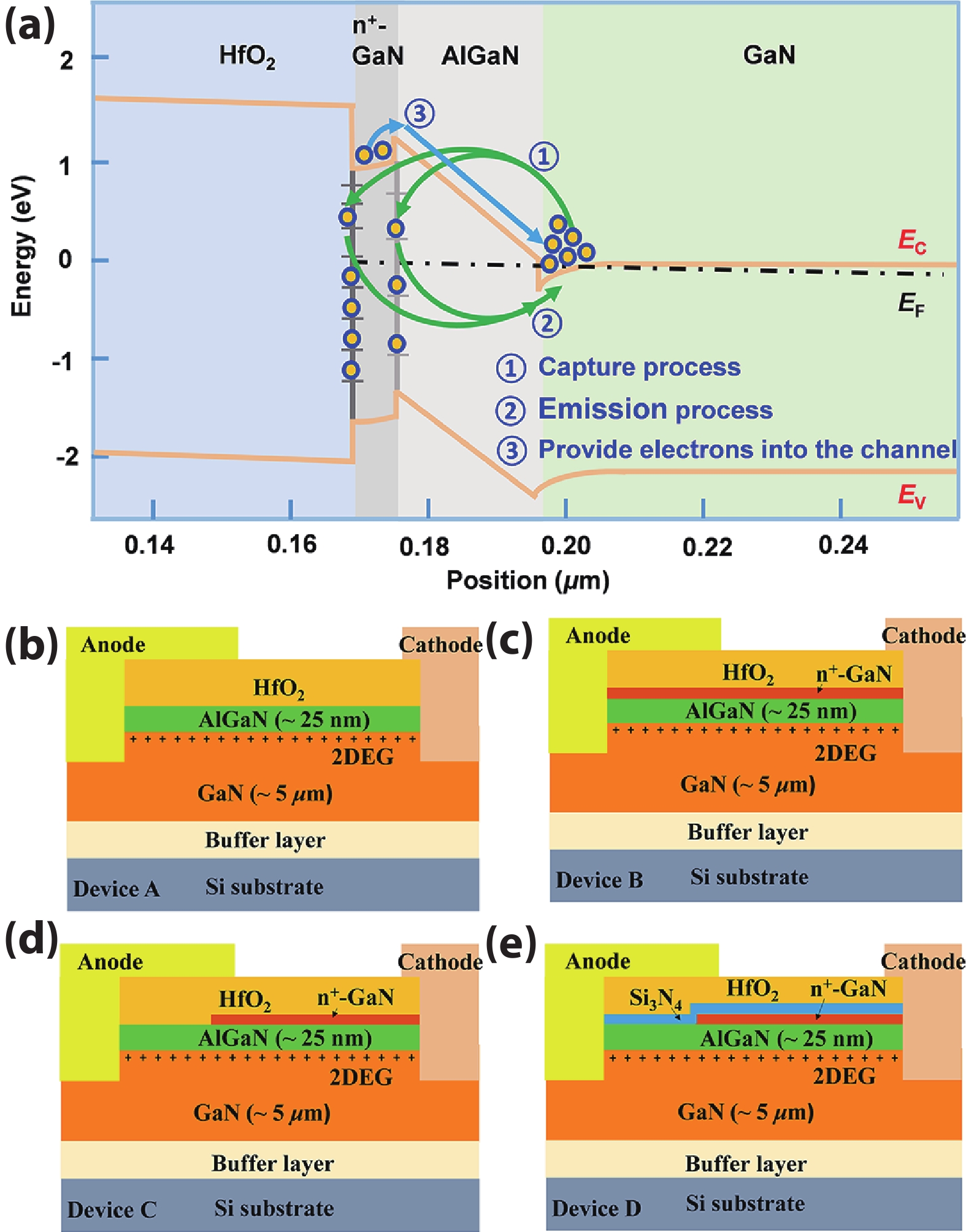
Fig. 1.  (Color online) (a) Schematic energy band diagram for the AlGaN/GaN SBD with an n+-GaN cap layer. Schematic cross-section for lateral AlGaN/GaN SBDs: (b) without n+-GaN cap layer, (c) with n+-GaN cap layer, (d) with partial n+-GaN cap layer, (e) with partial n+-GaN cap layer and Si3N4 protective layer.

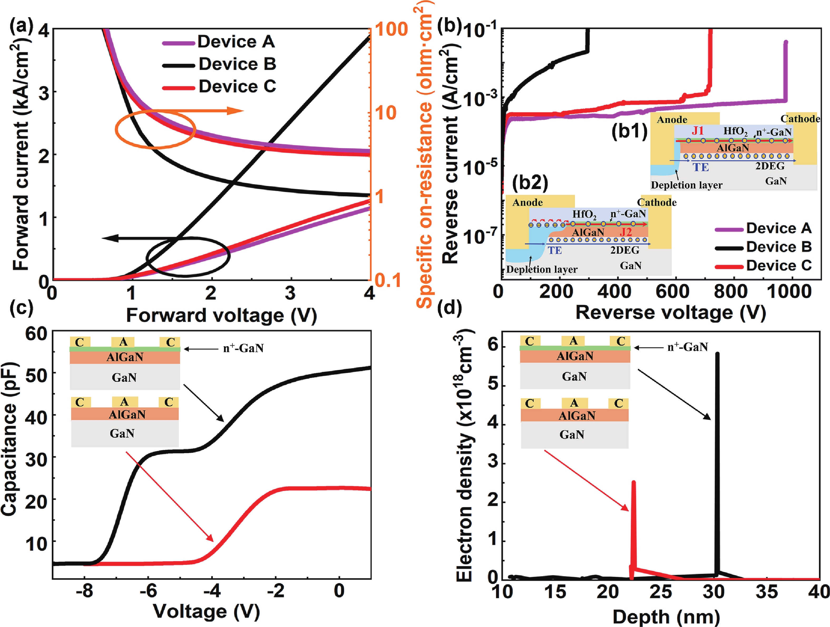
Fig. 2.  (Color online) (a) Forward current-voltage (JV) characteristics and Ron,sp, and (b) reverse blocking effect for Devices A, B and C. Insets (b1) and (b2) show leakage paths J1 and J2 for Devices B and C, respectively. (c) CV profiles in terms of the applied voltage, and (d) electron concentration profiles for AlGaN/GaN heterostructures with/without n+-GaN layer.

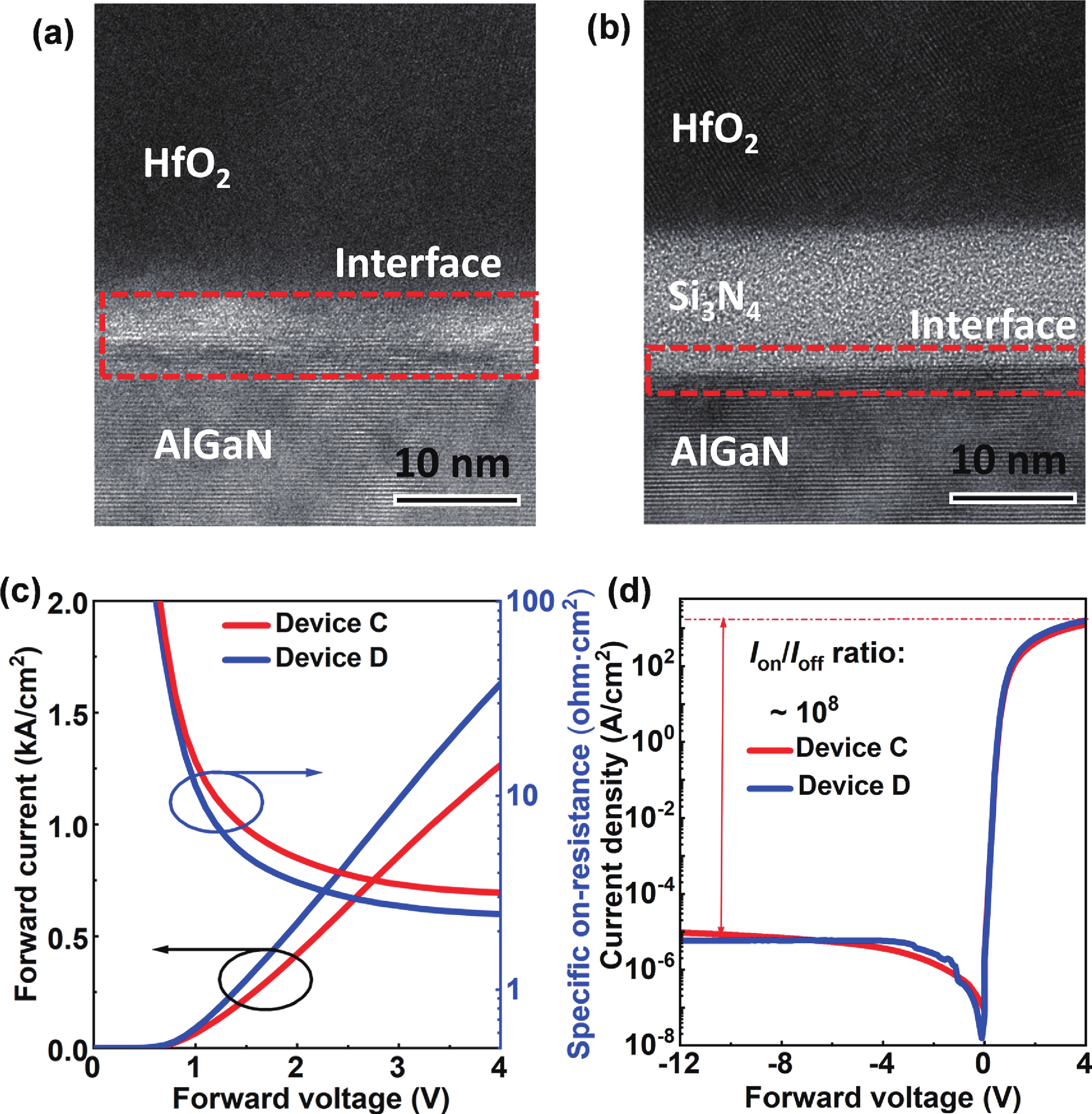
Fig. 3.  (Color online) Cross-sectional high-resolution transmission electron microscope micrographs for the lateral AlGaN/GaN SBDs with partial n+-GaN cap layer: (a) without Si3N4 protective layer, (b) with Si3N4 protective layer. (c) Experimental forward JV characteristics and Ron,sp for Devices C and D. (d) JV characteristics in semi-log scale for Devices C and D.

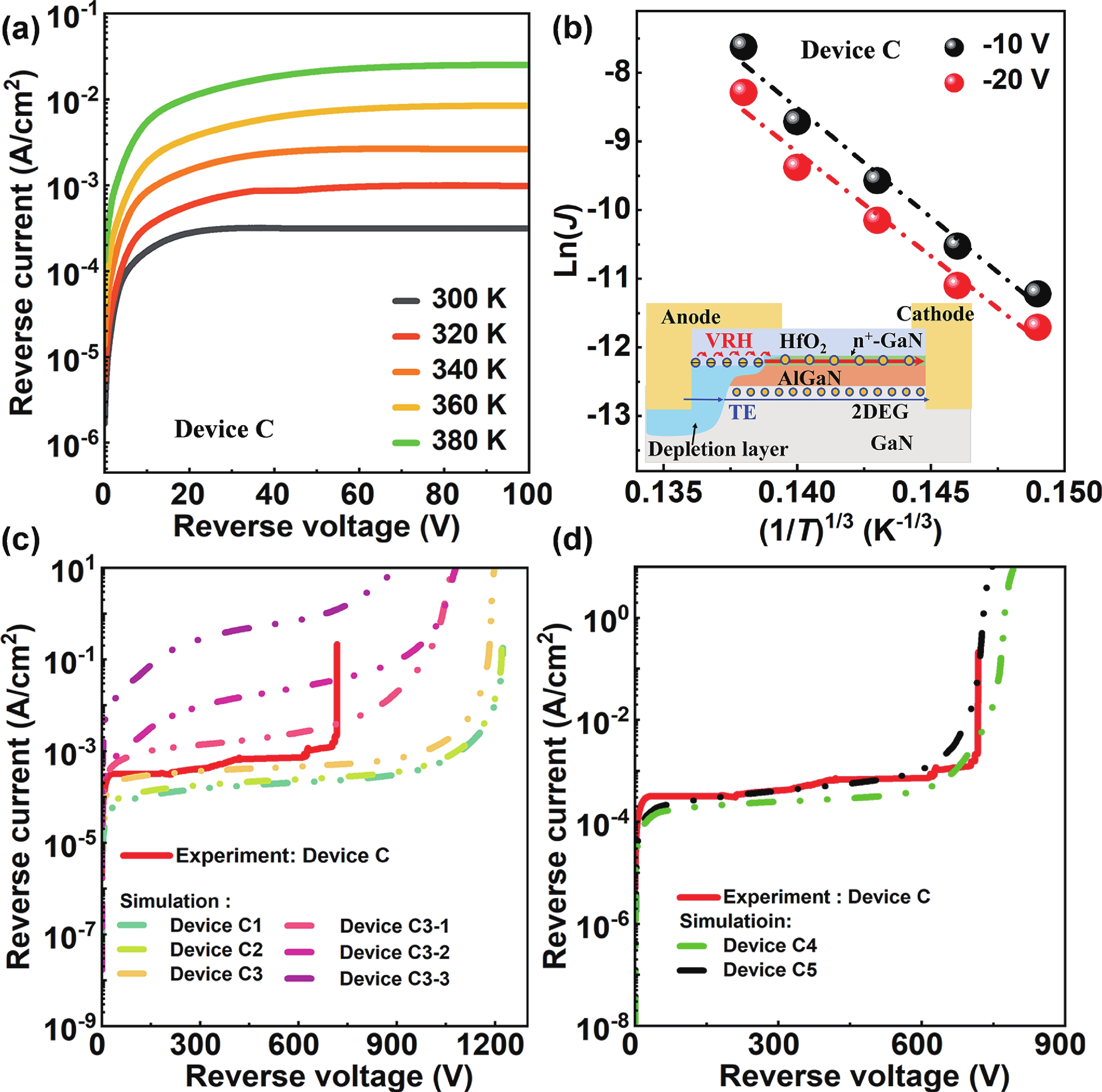
Fig. 4.  (Color online) (a) Temperature-dependent reverse JV characteristics of Device C from 300 to 380 K. (b) Linear relationship between Ln (J) and (1/T)1/3 for Device C. Inset figure shows leakage current models for Device C. (c) Reverse JV characteristics for Devices C, C1, C2, C3, C3−1, C3−2, and C3−3. (d) Reverse JV characteristics for Devices C, C4 and C5.

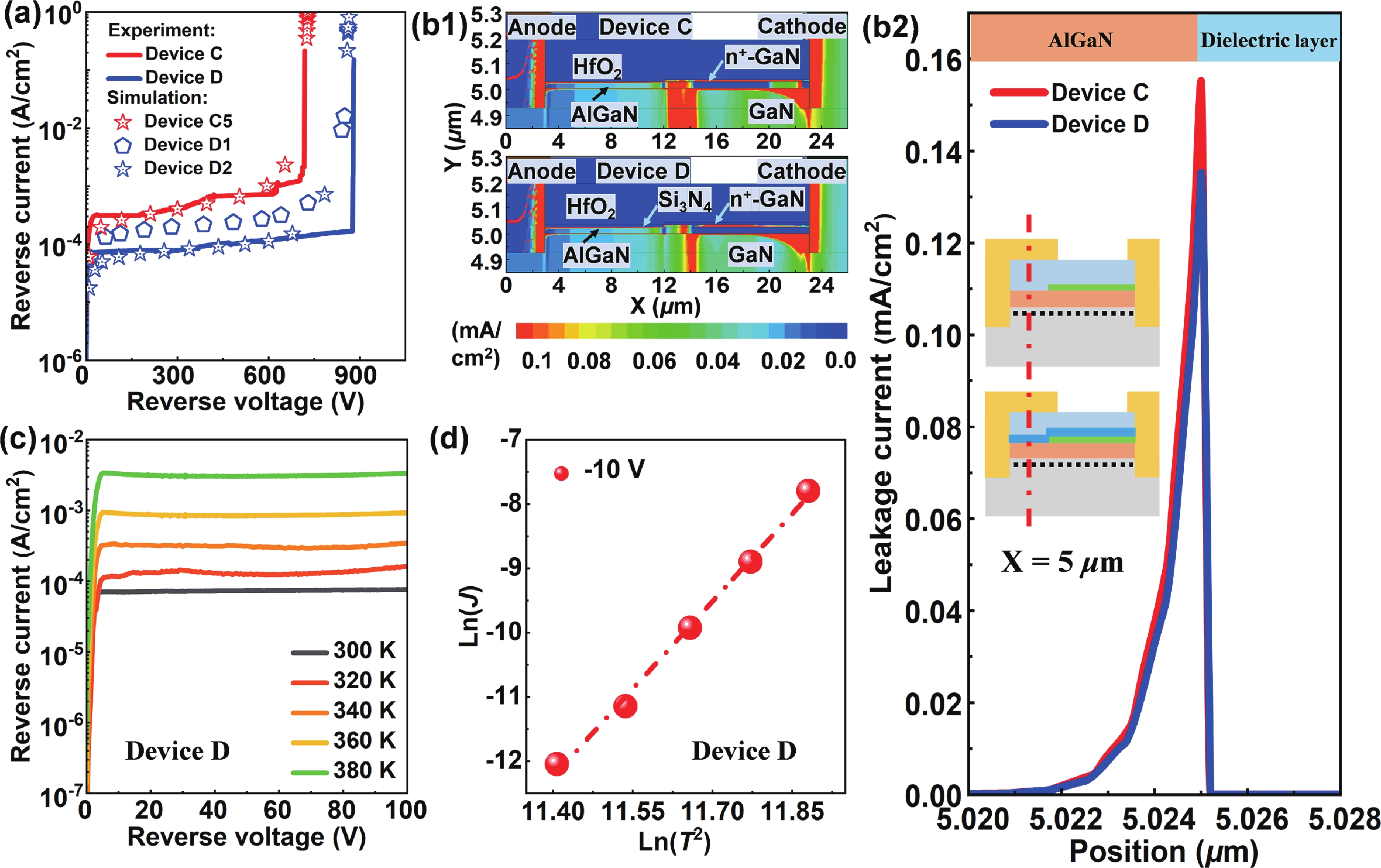
Fig. 5.  (Color online) (a) Experimental and simulated reverse JV characteristics for Devices C and D. Leakage current distribution profiles for Devices C and D: (b1) 2-D, (b2) 1-D. (c) Temperature-dependent reverse JV characteristics of the Device D from 300 to 400 K. (d) Linear relationship between Ln (J) and Ln (T2) for Device D.

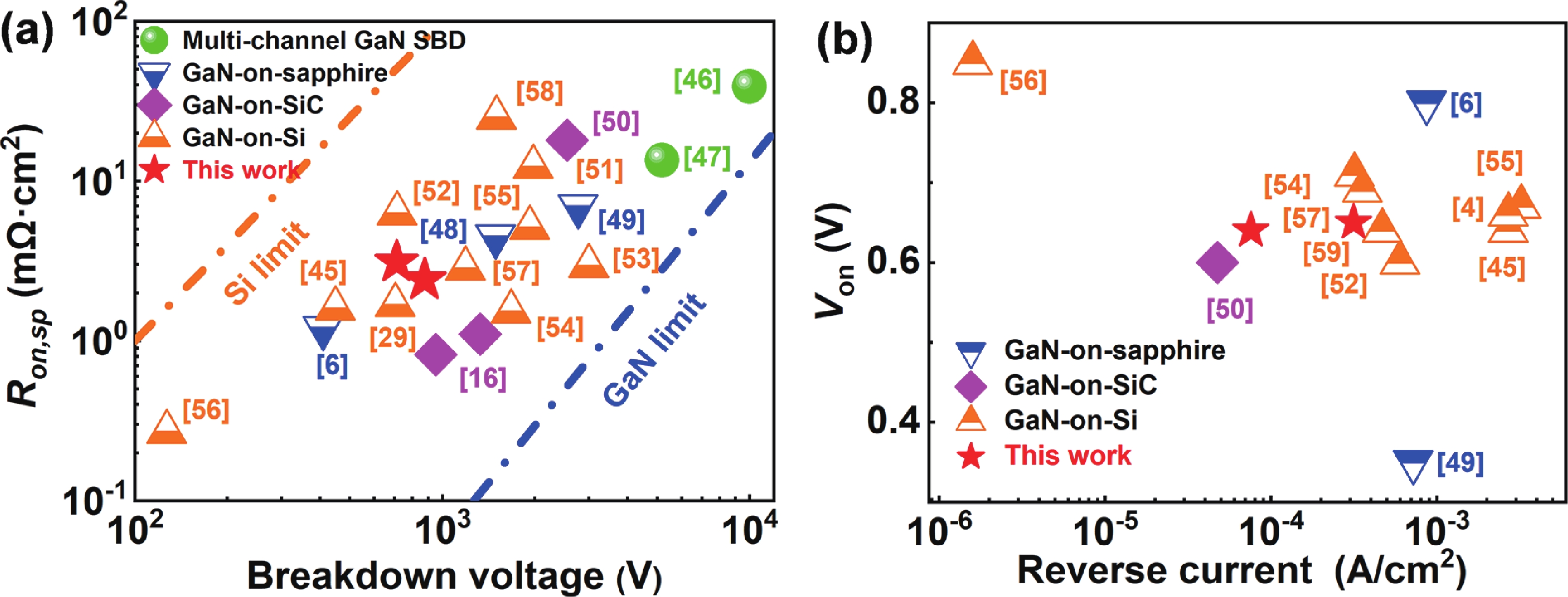
Fig. 6.  (Color online) Benchmark of (a) Ron,sp in terms of BV and (b) Von in terms of reverse current at the reverse voltage of −100 V for the fabricated Devices C and D in this work and other reported SBDs.

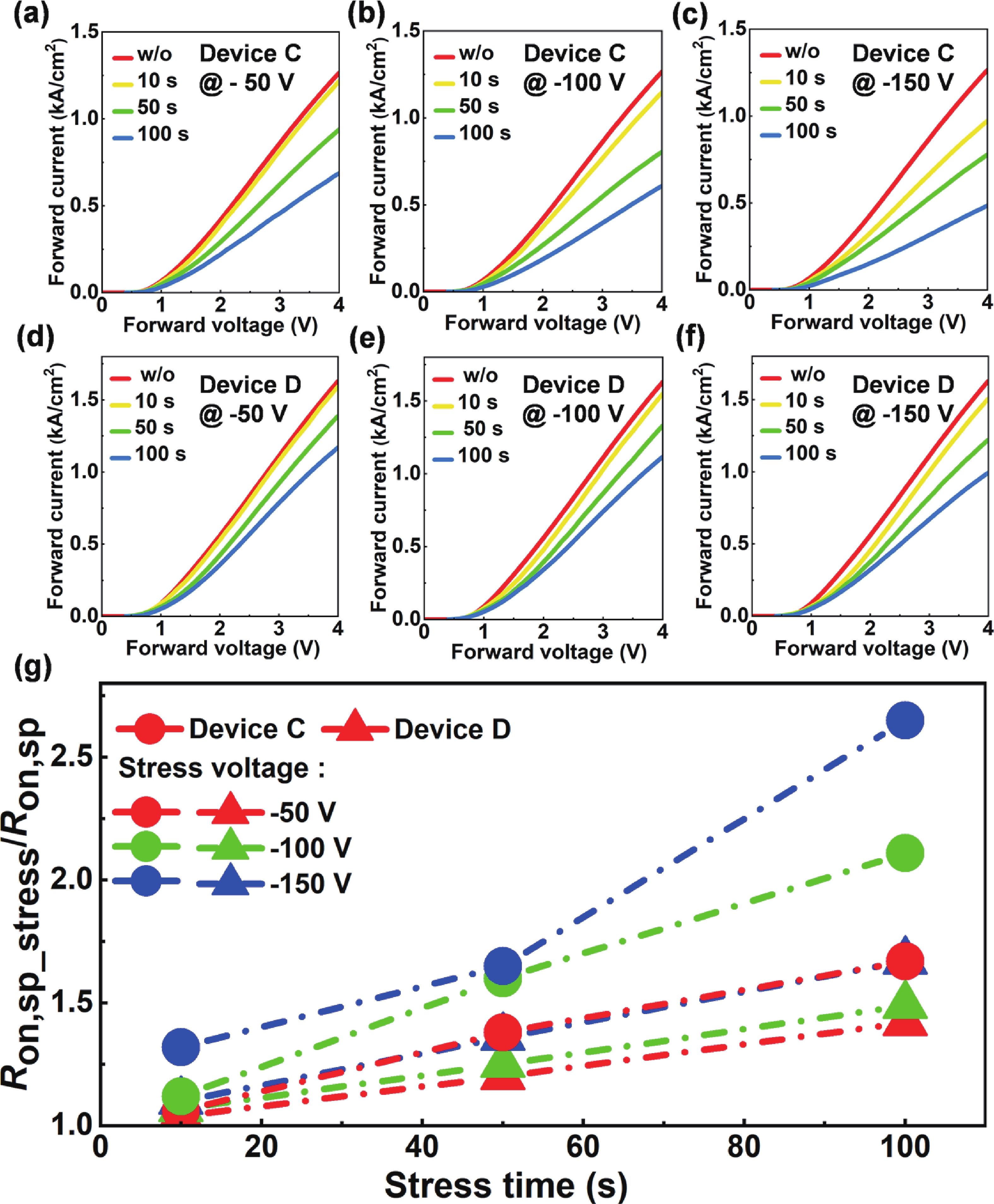
Fig. 7.  (Color online) (a) − (f) Electrical stress characteristics for Devices C and D with varying stress voltages of −50, −100 and −150 V, respectively. (g) Ron,sp_stress/Ron,sp in terms of stress time for Devices C and D at different stress voltages.

Table 1.   Trap information for GaN layers grown on different substrates.

Trap level (eV)Trap density (cm−3)Capture cross-section (cm2)SubstrateReference
Ec−0.239.5 × 10135.43 × 10−15Sapphire[34]
Ec−0.603.2 × 10141.61 × 10−15Sapphire[34]
Ec−0.173.5 × 10148.7 × 10−18Sapphire[35]
Ec−0.245.5 × 10142.6 × 10−18Sapphire[35]
Ec−0.598.5 × 10139.0 × 10−16Sapphire[35]
Ec−0.57~ 10163.0 × 10−15Silicon[36]
Ec−0.705.5 × 10143.0 × 10−15Silicon[33]
DownLoad: CSV

Table 2.   Structural information for different AlGaN/GaN SBDs.

Device No.Bulk trap density (cm−3)Interface trap density (cm−2)Impact ionization modelsExperiment
/Simulation
Substrate
Device AExperimentSilicon
Device B
Device C
Device C11.0 × 1013[40](1), (2)SimulationSapphire
Device C21.0 × 1014[40]
Device C31.0 × 1015[40]
Device C3−11.0 × 10151.0 × 1012[41]
Device C3−21.0 × 10¹⁴[42]
Device C3−31.0 × 10¹⁶[43]
Device C41.0 × 1015-(3), (4)SimulationSilicon
Device C51.0 × 1013[10]
Device DExperiment
Device D11.0 × 10151.0 × 1013(3), (4)Simulation
Device D2
DownLoad: CSV
[1]
Islam N, Mohamed M F P, Khan M F A J, et al. Reliability, applications and challenges of GaN HEMT technology for modern power devices: A review. Crystals, 2022, 12(11), 1581 doi: 10.3390/cryst12111581
[2]
Mounika B, Ajayan J, Bhattacharya S, et al. Recent developments in materials, architectures and processing of AlGaN/GaN HEMTs for future RF and power electronic applications: A critical review. Micro Nanostruct, 2022, 168, 207317 doi: 10.1016/j.micrna.2022.207317
[3]
Zhang T, Wang Y, Zhang Y N, et al. Comprehensive annealing effects on AlGaN/GaN Schottky barrier diodes with different work-function metals. IEEE Trans Electron Devices, 2021, 68(6), 2661 doi: 10.1109/TED.2021.3074896
[4]
Zhou Q, Jin Y, Shi Y Y, et al. High reverse blocking and low onset voltage AlGaN/GaN-on-Si lateral power diode with MIS-gated hybrid anode. IEEE Electron Device Lett, 2015, 36(7), 660 doi: 10.1109/LED.2015.2432171
[5]
Rajagopal Reddy V, Janardhanam V, Ju J W, et al. Electronic parameters and carrier transport mechanism of high-barrier Se Schottky contacts to n-type GaN. Solid State Commun, 2014, 179, 34 doi: 10.1016/j.ssc.2013.11.011
[6]
Yang X X, Cheng Z, Yu Z G, et al. The influence of anode trench geometries on electrical properties of AlGaN/GaN Schottky barrier diodes. Electronics, 2020, 9(2), 282 doi: 10.3390/electronics9020282
[7]
Wang T F, Zong Y, Nela L, et al. Enhancement-mode multi-channel AlGaN/GaN transistors with LiNiO junction tri-gate. IEEE Electron Device Lett, 2022, 43(9), 1523 doi: 10.1109/LED.2022.3189635
[8]
Nela L, Xiao M, Zhang Y H, et al. A perspective on multi-channel technology for the next-generation of GaN power devices. Appl Phys Lett, 2022, 120(19), 190501 doi: 10.1063/5.0086978
[9]
Li C K, Wu Y R. Study on the current spreading effect and light extraction enhancement of vertical GaN/InGaN LEDs. IEEE Trans Electron Devices, 2012, 59(2), 400 doi: 10.1109/TED.2011.2176132
[10]
Ibbetson J P, Fini P T, Ness K D, et al. Polarization effects, surface states, and the source of electrons in AlGaN/GaN heterostructure field effect transistors. Appl Phys Lett, 2000, 77(2), 250 doi: 10.1063/1.126940
[11]
Lee J H, Im K S, Lee J H. Effect of In-situ silicon carbon nitride (SiCN) cap layer on performances of AlGaN/GaN MISHFETs. IEEE J Electron Devices Soc, 2021, 9, 728 doi: 10.1109/JEDS.2021.3100760
[12]
Hsu L, Jones R E, Li S X, et al. Electron mobility in InN and III-N alloys. J Appl Phys, 2007, 102(7), 073705 doi: 10.1063/1.2785005
[13]
Wang J X, Yang S Y, Wang J, et al. Electron mobility limited by surface and interface roughness scattering in Al xGa1− xN/GaN quantum wells. Chin Phys B, 2013, 22(7), 077305 doi: 10.1088/1674-1056/22/7/077305
[14]
Ko T S, Lin D Y, Lin C F, et al. High-temperature carrier density and mobility enhancements in AlGaN/GaN HEMT using AlN spacer layer. J Cryst Growth, 2017, 464, 175 doi: 10.1016/j.jcrysgro.2016.12.023
[15]
Liu Z H, Ng G I, Zhou H, et al. Reduced surface leakage current and trapping effects in AlGaN/GaN high electron mobility transistors on silicon with SiN/Al2O3 passivation. Appl Phys Lett, 2011, 98(11), 113506 doi: 10.1063/1.3567927
[16]
Rahman M W, Chandrasekar H, Razzak T, et al. Hybrid BaTiO3/SiNx/AlGaN/GaN lateral Schottky barrier diodes with low turn-on and high breakdown performance. Appl Phys Lett, 2021, 119(1), 013504 doi: 10.1063/5.0055946
[17]
Huang F P, Wang Z Z, Chu C S, et al. MIS-based GaN Schottky barrier diodes: Interfacial conditions on the reverse and forward properties. IEEE Trans Electron Devices, 2022, 69(10), 5522 doi: 10.1109/TED.2022.3201831
[18]
Gao X C, He F, Huang F P, et al. Investigation into the impact of bulk defects in the drift layer on the electrical properties of GaN-based trench Schottky barrier diodes. Jpn J Appl Phys, 2024, 63(5), 054003 doi: 10.35848/1347-4065/ad40eb
[19]
Wong M S, Lee C M, Myers D J, et al. Size-independent peak efficiency of III-nitride micro-light-emitting-diodes using chemical treatment and sidewall passivation. Appl Phys Express, 2019, 12(9), 097004 doi: 10.7567/1882-0786/ab3949
[20]
Wang H Y, Mao W, Yang C, et al. Lateral AlGaN/GaN Schottky barrier diode with arrayed p-GaN islands termination. IEEE Trans Electron Devices, 2021, 68(12), 6046 doi: 10.1109/TED.2021.3118326
[21]
Xiao M, Du Z H, Xie J Q, et al. Lateral p-GaN/2DEG junction diodes by selective-area p-GaN trench-filling-regrowth in AlGaN/GaN. Appl Phys Lett, 2020, 116(5), 053503 doi: 10.1063/1.5139906
[22]
Dang K, Zhang J C, Zhou H, et al. Lateral GaN Schottky barrier diode for wireless high-power transfer application with high RF/DC conversion efficiency: From circuit construction and device technologies to system demonstration. IEEE Trans Ind Electron, 2020, 67(8), 6597 doi: 10.1109/TIE.2019.2939968
[23]
Huang F P, Chu C S, Wang Z Z, et al. 1.43 kV GaN-based MIS Schottky barrier diodes. J Phys D: Appl Phys, 2024, 57(18), 185102 doi: 10.1088/1361-6463/ad256c
[24]
Letts E, Hashimoto T, Ikari M, et al. Development of GaN wafers for solid-state lighting via the ammonothermal method. J Cryst Growth, 2012, 350(1), 66 doi: 10.1016/j.jcrysgro.2011.12.024
[25]
Wang B F, Liu L, Tian G, et al. Studying the effect of temperature and pressure on GaN crystals via the Na-flux method. CrystEngComm, 2024, 26(24), 3176 doi: 10.1039/D4CE00314D
[26]
Yang S, Han S W, Sheng K, et al. Dynamic on-resistance in GaN power devices: Mechanisms, characterizations, and modeling. IEEE J Emerg Sel Top Power Electron, 2019, 7(3), 1425 doi: 10.1109/JESTPE.2019.2925117
[27]
Zhong Y Z, Zhang J W, Wu S, et al. A review on the GaN-on-Si power electronic devices. Fundam Res, 2022, 2(3), 462 doi: 10.1016/j.fmre.2021.11.028
[28]
Li H, Bai Z Y, Yang L. Investigation of double RESURF P-GaN gate AlGaN/GaN heterostructure field-effect transistors with partial N-GaN channels. J Electron Mater, 2024, 53(5), 2562 doi: 10.1007/s11664-024-10987-0
[29]
Lei J C, Wei J, Tang G F, et al. 650-V double-channel lateral Schottky barrier diode with dual-recess gated anode. IEEE Electron Device Lett, 2018, 39(2), 260 doi: 10.1109/LED.2017.2783908
[30]
Xu J Y, Liu X, Xie B, et al. Correlation between reverse leakage current and electric field spreading in GaN vertical SBD with high-energy ion implanted guard rings. IEEE Trans Electron Devices, 2023, 70(4), 1745 doi: 10.1109/TED.2023.3241260
[31]
Chen H, Wang H Y, Sheng K. Vertical β-Ga2O3 Schottky barrier diodes with field plate assisted negative beveled termination and positive beveled termination. IEEE Electron Device Lett, 2023, 44(1), 21 doi: 10.1109/LED.2022.3222878
[32]
Wang Z Z, Huang F P, Chu C S, et al. 2.5 kV/1.95 GW/cm2 AlGaN/GaN-based lateral Schottky barrier diodes with a high-k field plate to reduce reverse current. IEEE Trans Electron Devices, 2024, 71(6), 3811 doi: 10.1109/TED.2024.3388377
[33]
Nguyen X S, Goh X L, Zhang L, et al. Deep level traps in GaN LEDs grown by metal organic vapour phase epitaxy on an 8 inch Si(111) substrate. Jpn J Appl Phys, 2016, 55(6), 060306 doi: 10.7567/JJAP.55.060306
[34]
Cho H K, Kim C S, Hong C H. Electron capture behaviors of deep level traps in unintentionally doped and intentionally doped n-type GaN. J Appl Phys, 2003, 94(3), 1485 doi: 10.1063/1.1586981
[35]
Soh C B, Chua S J, Lim H F, et al. Identification of deep levels in GaN associated with dislocations. J Phys Condens Matter, 2004, 16(34), 6305 doi: 10.1088/0953-8984/16/34/027
[36]
Lee I H, Polyakov A Y, Smirnov N B, et al. Spatial location of the Ec-0.6 eV electron trap in AlGaN/GaN heterojunctions. J Vac Sci Technol B, 2014, 32(5), 050602 doi: 10.1116/1.4895840
[37]
Cao L N, Wang J S, Harden G, et al. Experimental characterization of impact ionization coefficients for electrons and holes in GaN grown on bulk GaN substrates. Appl Phys Lett, 2018, 112(26), 262103 doi: 10.1063/1.5031785
[38]
Ambacher O, Smart J, Shealy J R, et al. Two-dimensional electron gases induced by spontaneous and piezoelectric polarization charges in N- and Ga-face AlGaN/GaN heterostructures. J Appl Phys, 1999, 85(6), 3222 doi: 10.1063/1.369664
[39]
Huang F P, Chu C S, Jia X Y, et al. Simulation study for GaN-based hybrid trench MOS barrier Schottky diode with an embedded p-type NiO termination: Increased forward current density and enhanced breakdown voltage. Jpn J Appl Phys, 2022, 61(1), 014002 doi: 10.35848/1347-4065/ac40cf
[40]
Tokuda Y. (invited) DLTS studies of defects in n-GaN. ECS Trans, 2016, 75(4), 39 doi: 10.1149/07504.0039ecst
[41]
Faraz S M, Ashraf H, Imran Arshad M, et al. Interface state density of free-standing GaN Schottky diodes. Semicond Sci Technol, 2010, 25(9), 095008 doi: 10.1088/0268-1242/25/9/095008
[42]
Jackson C M, Arehart A R, Cinkilic E, et al. Interface trap characterization of atomic layer deposition Al2O3/GaN metal-insulator-semiconductor capacitors using optically and thermally based deep level spectroscopies. J Appl Phys, 2013, 113(20), 204505 doi: 10.1063/1.4808093
[43]
Aoshima K, Taoka N, Horita M, et al. SiO2/GaN interfaces with low defect densities and high breakdown electric fields formed by plasma-enhanced atomic layer deposition. Jpn J Appl Phys, 2022, 61, SC1073 doi: 10.35848/1347-4065/ac4f79
[44]
Kotani J, Tajima M, Kasai S, et al. Mechanism of surface conduction in the vicinity of Schottky gates on AlGaN / GaN heterostructures. Appl Phys Lett, 2007, 91(9), 093501 doi: 10.1063/1.2775834
[45]
Zhang T, Zhang J C, Zhang W H, et al. Investigation of an AlGaN-channel Schottky barrier diode on a silicon substrate with a molybdenum anode. Semicond Sci Technol, 2021, 36(4), 044003 doi: 10.1088/1361-6641/abcbd5
[46]
Xiao M, Ma Y W, Liu K, et al. 10 kV, 39 mΩ·cm2 multi-channel AlGaN/GaN Schottky barrier diodes. IEEE Electron Device Lett, 2021, 42(6), 808 doi: 10.1109/LED.2021.3076802
[47]
Xiao M, Ma Y, Du Z, et al. 5 kV Multi-Channel AlGaN/GaN Power Schottky Barrier Diodes with Junction-Fin-Anode. 2020 IEEE International Electron Devices Meeting (IEDM), 2020, 5.4.1
[48]
Wang T T, Wang X, Cui Z H, et al. Metal-nitride dual-anode AlGaN/GaN heterostructure Schottky barrier diodes with tunable turn-on voltage and reverse leakage current. Semicond Sci Technol, 2022, 37(4), 045013 doi: 10.1088/1361-6641/ac5676
[49]
Lu Y, Zhou F, Xu W Z, et al. Multi-aperture anode based AlGaN/GaN Schottky barrier diodes with low turn-on voltage and high uniformity. Appl Phys Express, 2020, 13(9), 096502 doi: 10.35848/1882-0786/abaf0e
[50]
Zhang T, Zhang Y N, Li R H, et al. Current transport mechanism of AlGaN-channel Schottky barrier diode with extremely low leakage current and high blocking voltage of 2.55 kV. Appl Phys Lett, 2022, 120(9), 092102 doi: 10.1063/5.0077691
[51]
Deng S, Liu K, Wang C, et al. The influence of recessed floating metal rings structure on electrical properties of AlGaN/GaN Schottky barrier diodes. Phys Status Solidi A, 2022, 219(2), 2100502 doi: 10.1002/pssa.202100502
[52]
Hsueh K P, Chang Y S, Li B H, et al. Effect of the AlGaN/GaN Schottky barrier diodes combined with a dual anode metal and a p-GaN layer on reverse breakdown and turn-on voltage. Mater Sci Semicond Process, 2019, 90, 107 doi: 10.1016/j.mssp.2018.10.013
[53]
Zhang T, Zhang J C, Zhou H, et al. A >3 kV/2.94 mΩ·cm2 and low leakage current with low turn-on voltage lateral GaN Schottky barrier diode on silicon substrate with anode engineering technique. IEEE Electron Device Lett, 2019, 40(10), 1583 doi: 10.1109/LED.2019.2933314
[54]
Xu R, Chen P, Liu M H, et al. 2.7-kV AlGaN/GaN Schottky barrier diode on silicon substrate with recessed-anode structure. Solid State Electron, 2021, 175, 107953 doi: 10.1016/j.sse.2020.107953
[55]
Zhu M D, Song B, Qi M, et al. 1.9-kV AlGaN/GaN lateral Schottky barrier diodes on silicon. IEEE Electron Device Lett, 2015, 36(4), 375 doi: 10.1109/LED.2015.2404309
[56]
Matioli E, Lu B, Palacios T. Ultralow leakage Current AlGaN/GaN Schottky diodes with 3-D anode structure. IEEE Trans Electron Devices, 2013, 60(10), 3365 doi: 10.1109/TED.2013.2279120
[57]
Gao J N, Jin Y F, Xie B, et al. Low ON-resistance GaN Schottky barrier diode with high VON uniformity using LPCVD Si3N4 compatible self-terminated, low damage anode recess technology. IEEE Electron Device Lett, 2018, 39(6), 859 doi: 10.1109/LED.2018.2830998
[58]
Boles T, Varmazis C, Carlson D, et al. >1200 V GaN-on-silicon Schottky diode. Phys Status Solidi C, 2013, 10(5), 835. doi: 10.1002/pssc.201200589
[59]
Gao J N, Wang M J, Yin R Y, et al. Schottky-MOS hybrid anode AlGaN/GaN lateral field-effect rectifier with low onset voltage and improved breakdown voltage. IEEE Electron Device Lett, 2017, 38(10), 1425 doi: 10.1109/LED.2017.2737520
[60]
Maeda T, Narita T, Yamada S, et al. Impact ionization coefficients and critical electric field in GaN. J Appl Phys, 2021, 129(18), 185702 doi: 10.1063/5.0050793
[61]
Ji D, Ercan B, Chowdhury S. Experimental determination of impact ionization coefficients of electrons and holes in gallium nitride using homojunction structures. Appl Phys Lett, 2019, 115(7), 073503 doi: 10.1063/1.5099245
  • Search

    Advanced Search >>

    GET CITATION

    shu

    Export: BibTex EndNote

    Article Metrics

    Article views: 131 Times PDF downloads: 23 Times Cited by: 0 Times

    History

    Received: 19 January 2025 Revised: 17 March 2025 Online: Accepted Manuscript: 10 April 2025

    Catalog

      Email This Article

      User name:
      Email:*请输入正确邮箱
      Code:*验证码错误
      Zhizhong Wang, Jingting He, Fuping Huang, Xuchen Gao, Kangkai Tian, Chunshuang Chu, Yonghui Zhang, Shuting Cai, Xiaojuan Sun, Dabing Li, Xiao Wei Sun, Zi-Hui Zhang. AlGaN/GaN-based SBDs grown on silicon substrates with trenched n+-GaN cap layer and local passivation layer to improve BFOM and dynamic properties[J]. Journal of Semiconductors, 2025, In Press. doi: 10.1088/1674-4926/25010024 ****Z Z Wang, J T He, F P Huang, X C Gao, K K Tian, C S Chu, Y H Zhang, S T Cai, X J Sun, D B Li, X W Sun, and Z-H Zhang, AlGaN/GaN-based SBDs grown on silicon substrates with trenched n+-GaN cap layer and local passivation layer to improve BFOM and dynamic properties[J]. J. Semicond., 2025, accepted doi: 10.1088/1674-4926/25010024
      Citation:
      Zhizhong Wang, Jingting He, Fuping Huang, Xuchen Gao, Kangkai Tian, Chunshuang Chu, Yonghui Zhang, Shuting Cai, Xiaojuan Sun, Dabing Li, Xiao Wei Sun, Zi-Hui Zhang. AlGaN/GaN-based SBDs grown on silicon substrates with trenched n+-GaN cap layer and local passivation layer to improve BFOM and dynamic properties[J]. Journal of Semiconductors, 2025, In Press. doi: 10.1088/1674-4926/25010024 ****
      Z Z Wang, J T He, F P Huang, X C Gao, K K Tian, C S Chu, Y H Zhang, S T Cai, X J Sun, D B Li, X W Sun, and Z-H Zhang, AlGaN/GaN-based SBDs grown on silicon substrates with trenched n+-GaN cap layer and local passivation layer to improve BFOM and dynamic properties[J]. J. Semicond., 2025, accepted doi: 10.1088/1674-4926/25010024

      AlGaN/GaN-based SBDs grown on silicon substrates with trenched n+-GaN cap layer and local passivation layer to improve BFOM and dynamic properties

      DOI: 10.1088/1674-4926/25010024
      CSTR: 32376.14.1674-4926.25010024
      More Information
      • Zhizhong Wang got his bachelor’ degree in 2012 from Shanxi Datong University and his master’s degree in 2019 from Shenyang University of Technology. He is currently a Ph.D. candidate at Hebei University of Technology under the supervision of Prof. Zi-Hui Zhang. His research primarily focuses on the fabrication and analysis of gallium nitride power semiconductor devices
      • Zi-Hui Zhang received his Ph.D. from Nanyang Technological University. He is a professor at the State Key Laboratory of Reliability and Intelligence of Electrical Equipment, Hebei University of Technology and Guangdong University of Technology. He is also a “100-Talent-Plan” Distinguished Professor of Hebei Province. His research interests include III-nitride-based semiconductor materials and devices
      • Corresponding author: zh.zhang@hebut.edu.cn
      • Received Date: 2025-01-19
      • Revised Date: 2025-03-17
      • Available Online: 2025-04-10

      Catalog

        /

        DownLoad:  Full-Size Img  PowerPoint
        Return
        Return