


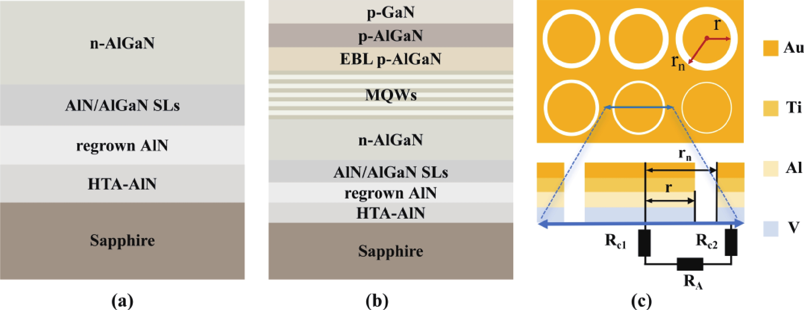
Fig. 1.
(Color online) (a) and (b) are the epitaxial structures of the n-AlGaN and the far-UVC LED wafers. (c) Schematic diagram of the n-electrode for the CTLM.
ARTICLES
Jiale Peng1, 2, Ke Jiang1, 2, , Shanli Zhang1, 2, , Jianwei Ben1, 2, Kexi Liu1, 2, Ziyue Qin1, 2, Ruihua Chen1, 2, Chunyue Zhang1, 2, Shunpeng Lv1, 2, Xiaojuan Sun1, 2 and Dabing Li1, 2
Corresponding author: Ke Jiang, jiangke@ciomp.ac.cn; Shanli Zhang, zhangshanli@ciomp.ac.cn
Abstract: AlGaN-based LEDs with peak wavelength below 240 nm (far-UVC) pose no significant harm to human health, thus highlighting their broader application potential. While, there is a significant Schottky barrier between the n-electrode and Al-rich n-AlGaN, adversely impeding electron injection and resulting in considerable heat generation. Here, we fabricate V-based electrodes of V/Al/Ti/Au on n-AlGaN with Al content over 80% and investigate the relationship between the metal diffusion and contact properties during the high-temperature annealing process. Experiments reveal that decreasing V thickness in the electrode promotes the diffusion of Al towards the surface of n-AlGaN, which facilitates the formation of VN and thus the increase of local electron concentration, resulting in lower specific contact resistivity. Then, increasing the Al thickness inhibits the diffusion of Au to the n-AlGaN surface, suppressing the rise of Schottky barrier. Experimentally, an optimized n-electrode of V(10 nm)/Al(240 nm)/Ti(40 nm)/Au(50 nm) on n-Al0.81Ga0.19N is obtained, realizing an optimal specific contact resistivity of 7.30 × 10⁻⁴ Ω·cm2. Based on the optimal n-electrode preparation scheme for Al-rich n-AlGaN, the work voltage of a far-UVC LED with peak wavelength of 233.5 nm is effectively reduced.
Keywords: Al-rich n-AlGaN, specific contact resistivity, far-UVC LED
| [1] |
Zollner C J, DenBaars S P, Speck J S, et al. Germicidal ultraviolet LEDs: A review of applications and semiconductor technologies. Semicond Sci Technol, 2021, 36(12), 123001 doi: 10.1088/1361-6641/ac27e7
|
| [2] |
Rauch K D, MacIsaac S A, Reid B, et al. A critical review of ultra-violet light emitting diodes as a one water disinfection technology. Water Res X, 2024, 25, 100271 doi: 10.1016/j.wroa.2024.100271
|
| [3] |
Zhang L, Fang Z B, Li J X, et al. Research progress on environmental stability of SARS-CoV-2 and influenza viruses. Front Microbiol, 2024, 15, 1463056 doi: 10.3389/fmicb.2024.1463056
|
| [4] |
Wang C X, Song X F, Shen J Y, et al. Recent advances in DNA-based nanoprobes for in vivo MiRNA imaging. Chemistry, 2024, 30(66), e202402566 doi: 10.1002/chem.202402566
|
| [5] |
Urban L, Charles F, de Miranda M R A, et al. Understanding the physiological effects of UV-C light and exploiting its agronomic potential before and after harvest. Plant Physiol Biochem, 2016, 105, 1 doi: 10.1016/j.plaphy.2016.04.004
|
| [6] |
Zwicker P, Schleusener J, Lohan S B, et al. Application of 233 nm far-UVC LEDs for eradication of MRSA and MSSA and risk assessment on skin models. Sci Rep, 2022, 12, 2587 doi: 10.1038/s41598-022-06397-z
|
| [7] |
Fukui T, Niikura T, Oda T, et al. Safety of 222 nm UVC irradiation to the surgical site in a rabbit model. Photochem Photobiol, 2022, 98(6), 1365 doi: 10.1111/php.13620
|
| [8] |
Buonanno M, Ponnaiya B, Welch D, et al. Germicidal efficacy and mammalian skin safety of 222-nm UV light. Radiat Res, 2017, 187(4), 483 doi: 10.1667/RR0010CC.1
|
| [9] |
Li J C, Gao N, Cai D J, et al. Multiple fields manipulation on nitride material structures in ultraviolet light-emitting diodes. Light Sci Appl, 2021, 10, 129 doi: 10.1038/s41377-021-00563-0
|
| [10] |
Moe C G, Sugiyama S, Kasai J, et al. AlGaN light-emitting diodes on AlN substrates emitting at 230 nm. Phys Status Solidi A, 2018, 215(10), 1700660 doi: 10.1002/pssa.201700660
|
| [11] |
Cai Q, You H F, Guo H, et al. Progress on AlGaN-based solar-blind ultraviolet photodetectors and focal plane arrays. Light Sci Appl, 2021, 10(1), 94 doi: 10.1038/s41377-021-00527-4
|
| [12] |
Pandey A, Gim J, Hovden R, et al. Electron overflow of AlGaN deep ultraviolet light emitting diodes. Appl Phys Lett, 2021, 118(24), 241109 doi: 10.1063/5.0055326
|
| [13] |
Mehnke F, Kuhn C, Guttmann M, et al. Efficient charge carrier injection into sub-250 nm AlGaN multiple quantum well light emitting diodes. Appl Phys Lett, 2014, 105(5), 051113 doi: 10.1063/1.4892883
|
| [14] |
Hiroki M, Taniyasu Y, Kumakura K. High-temperature performance of AlN MESFETs with epitaxially grown n-type AlN channel layers. IEEE Electron Device Lett, 2022, 43(3), 350 doi: 10.1109/LED.2022.3141100
|
| [15] |
Ebata K, Nishinaka J, Taniyasu Y, et al. High hole concentration in Mg-doped AlN/AlGaN superlattices with high Al content. Jpn J Appl Phys, 2018, 57(4S), 04FH09 doi: 10.7567/JJAP.57.04FH09
|
| [16] |
Wang J M, Wang M X, Xu F J, et al. Sub-nanometer ultrathin epitaxy of AlGaN and its application in efficient doping. Light Sci Appl, 2022, 11(1), 71 doi: 10.1038/s41377-022-00753-4
|
| [17] |
Jiang K, Sun X J, Shi Z M, et al. Quantum engineering of non-equilibrium efficient p-doping in ultra-wide band-gap nitrides. Light Sci Appl, 2021, 10(1), 69 doi: 10.1038/s41377-021-00503-y
|
| [18] |
Zhang C Y, Jiang K, Sun X J, et al. Recent progress on AlGaN based deep ultraviolet light-emitting diodes below 250 nm. Crystals, 2022, 12(12), 1812 doi: 10.3390/cryst12121812
|
| [19] |
Mehnke F, Sulmoni L, Guttmann M, et al. Influence of light absorption on the performance characteristics of UV LEDs with emission between 239 and 217 nm. Appl Phys Express, 2019, 12(1), 012008 doi: 10.7567/1882-0786/aaf788
|
| [20] |
France R, Xu T, Chen P P, et al. Vanadium-based Ohmic contacts to n-AlGaN in the entire alloy composition. Appl Phys Lett, 2007, 90(6), 062115 doi: 10.1063/1.2458399
|
| [21] |
Patsalas P, Kalfagiannis N, Kassavetis S, et al. Conductive nitrides: Growth principles, optical and electronic properties, and their perspectives in photonics and plasmonics. Mater Sci Eng R Rep, 2018, 123, 1 doi: 10.1016/j.mser.2017.11.001
|
| [22] |
Wu C I, Kahn A. Electronic states at aluminum nitride (0001)-1 × 1 surfaces. Appl Phys Lett, 1999, 74(4), 546 doi: 10.1063/1.123140
|
| [23] |
Kozawa T, Mori T, Ohwaki T, et al. UV photoemission study of AlGaN grown by metalorganic vapor phase epitaxy. Jpn J Appl Phys, 2000, 39(8A), L772 doi: 10.1143/JJAP.39.L772
|
| [24] |
Grabowski S P, Schneider M, Nienhaus H, et al. Electron affinity of AlxGa1–xN(0001) surfaces. Appl Phys Lett, 2001, 78(17), 2503 doi: 10.1063/1.1367275
|
| [25] |
Ye M Y, Hao X R, Zeng J F, et al. Research progress of alkaline earth metal iron-based oxides as anodes for lithium-ion batteries. J Semicond, 2024, 45(2), 021801 doi: 10.1088/1674-4926/45/2/021801
|
| [26] |
Kataoka K, Narita T, Yagi Y, et al. Comprehensive study of electron conduction and its compensation for degenerate Si-doped AlN-rich AlGaN. Physica Rapid Research Ltrs, 2024, 18(2), 2300055 doi: 10.1002/pssr.202300055
|
| [27] |
Mehnke F, Wernicke T, Pingel H, et al. Highly conductive n-AlxGa1–xN layers with aluminum mole fractions above 80%. Appl Phys Lett, 2013, 103(21), 212109 doi: 10.1063/1.4833247
|
| [28] |
Collazo R, Mita S, Xie J Q, et al. Progress on n-type doping of AlGaN alloys on AlN single crystal substrates for UV optoelectronic applications. Phys Status Solidi C, 2011, 8(7/8), 2031 doi: 10.1002/pssc.201000964
|
| [29] |
Moses P G, Miao M S, Yan Q M, et al. Hybrid functional investigations of band gaps and band alignments for AlN, GaN, InN, and InGaN. J Chem Phys, 2011, 134(8), 084703 doi: 10.1063/1.3548872
|
| [30] |
Yang Y, Xiong F B, Lin H Y, et al. Evaluation of Ti/Al/Ni/Au ohmic contact to n-AlGaN with different Ti/Al thickness for deep ultraviolet light emitting diode. Solid State Electron, 2023, 208, 108752 doi: 10.1016/j.sse.2023.108752
|
| [31] |
Zhao X Y, Sun K, Lv Z X, et al. Contact engineering of III-nitrides and metal schemes toward efficient deep-ultraviolet light-emitting diodes. ACS Appl Mater Interfaces, 2024, 16(5), 6605 doi: 10.1021/acsami.3c15303
|
| [32] |
Wang L, Mohammed F M, Adesida I. Differences in the reaction kinetics and contact formation mechanisms of annealed Ti∕Al/Mo/Au Ohmic contacts on n-GaN and AlGaN∕GaN epilayers. J Appl Phys, 2007, 101(1), 013702 doi: 10.1063/1.2402791
|
| [33] |
Van Daele B, Van Tendeloo G, Ruythooren W, et al. The role of Al on Ohmic contact formation on n-type GaN and AlGaN∕GaN. Appl Phys Lett, 2005, 87(6), 061905 doi: 10.1063/1.2008361
|
| [34] |
Miller M A, Koo B H, Bogart K H A, et al. Ti/Al/Ti/Au and V/Al/V/Au contacts to plasma-etched n-Al0.58Ga0.42N. J Electron Mater, 2008, 37(5), 564 doi: 10.1007/s11664-007-0300-8
|
| [35] |
Wang L, Mohammed F M, Adesida I. Formation mechanism of ohmic contacts on AlGaN/GaN heterostructure: Electrical and microstructural characterizations. J Appl Phys, 2008, 103(9), 093516 doi: 10.1063/1.2903482
|
| [36] |
Ebata K, Hiroki M, Tateno K, et al. Effects of thermal annealing on V-based ohmic contacts on n-type AlGaN with high Al content. Phys Status Solidi A, 2024, 221(21), 2400148 doi: 10.1002/pssa.202400148
|
| [37] |
Guo X Q, Xu F J, Lang J, et al. Influence of the barrier layer on the electrical properties of the V/Al-based Ohmic contact on n-type high-Al-fraction AlGaN. Appl Phys Lett, 2024, 124(23), 232106 doi: 10.1063/5.0208669
|
| [38] |
Sulmoni L, Mehnke F, Mogilatenko A, et al. Electrical properties and microstructure formation of V/Al-based n-contacts on high Al mole fraction n-AlGaN layers. Photon Res, 2020, 8(8), 1381 doi: 10.1364/PRJ.391075
|
| [39] |
Cho H K, Rass J, Mogilatenko A, et al. Impact of plasma treatment of n-Al0.87Ga0.13N: Si surfaces on V/Al/Ni/Au contacts in far-UVC LEDs. IEEE Photonics Technol Lett, 2023, 35(17), 915 doi: 10.1109/LPT.2023.3288216
|
| [40] |
Srivastava S, Hwang S M, Islam M, et al. Ohmic contact to high-aluminum-content AlGaN epilayers. J Electron Mater, 2009, 38(11), 2348 doi: 10.1007/s11664-009-0924-y
|
| [41] |
Jung S M, Lee C T, Shin M W. Investigation of V-Ti/Al/Ni/Au Ohmic contact to AlGaN/GaN heterostructures with a thin GaN cap layer. Semicond Sci Technol, 2015, 30(7), 075012 doi: 10.1088/0268-1242/30/7/075012
|
| [42] |
Schmid A, Schroeter C, Otto R, et al. Microstructure of V-based ohmic contacts to AlGaN/GaN heterostructures at a reduced annealing temperature. Appl Phys Lett, 2015, 106(5), 053509 doi: 10.1063/1.4907735
|
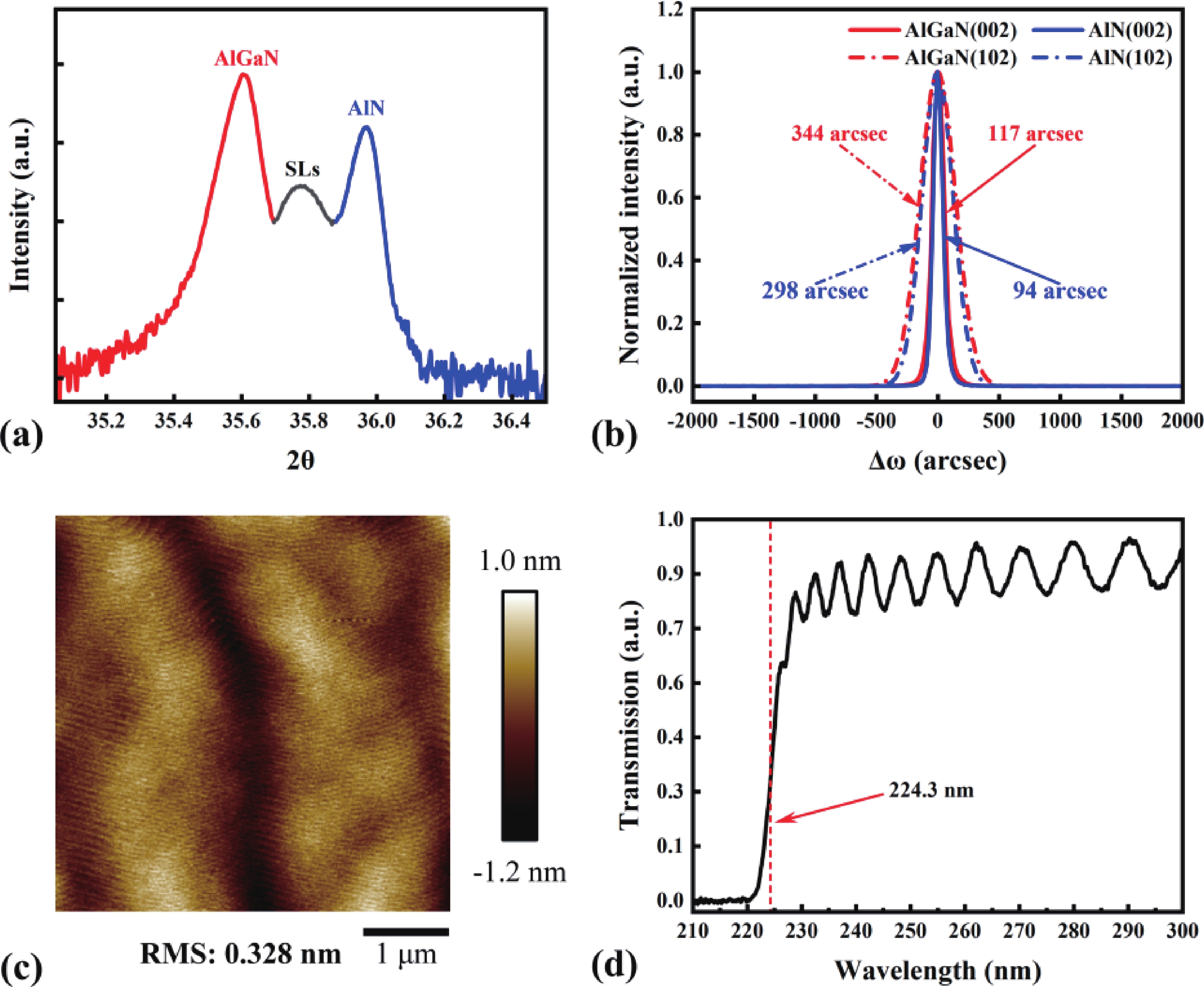
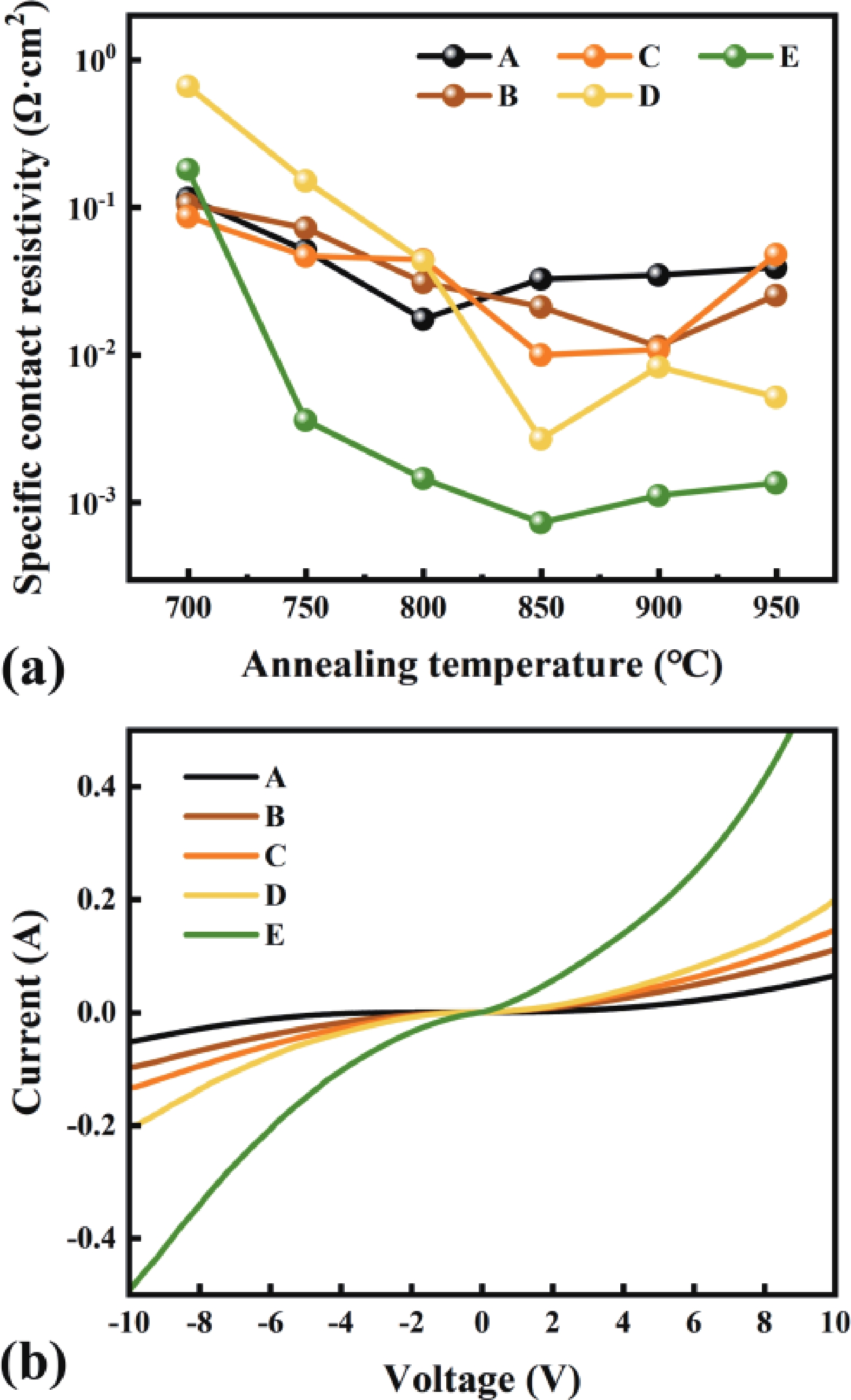
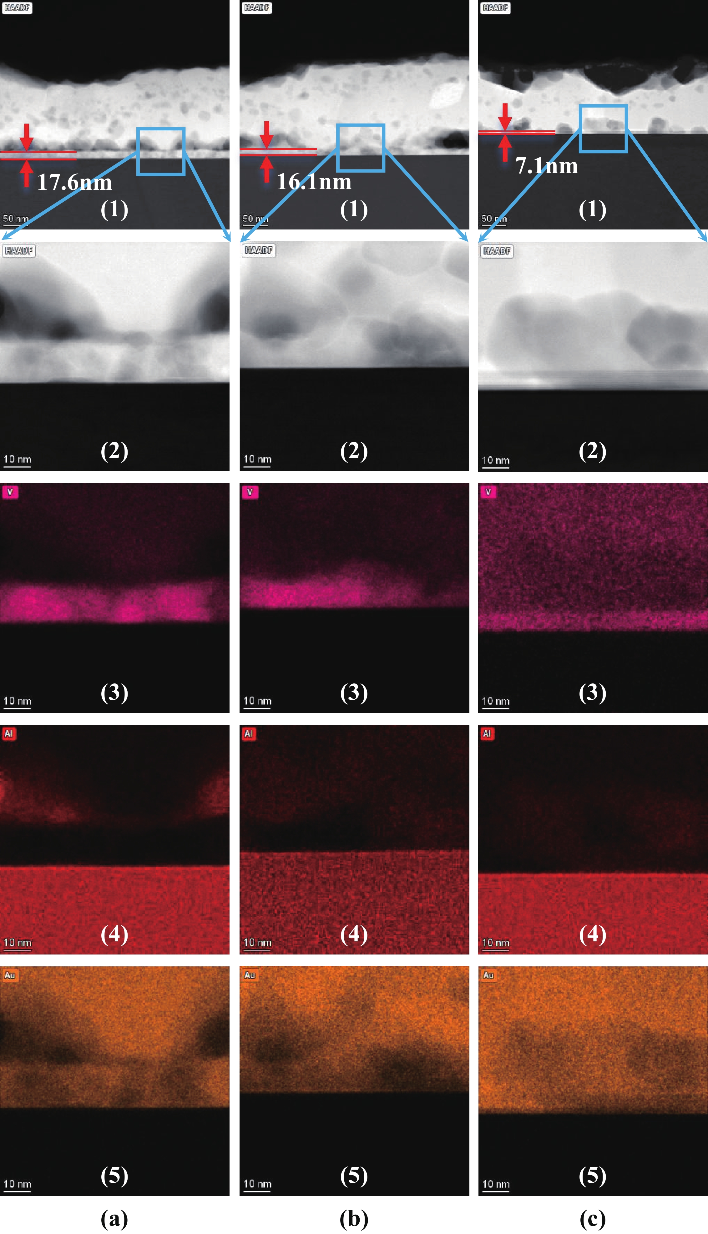
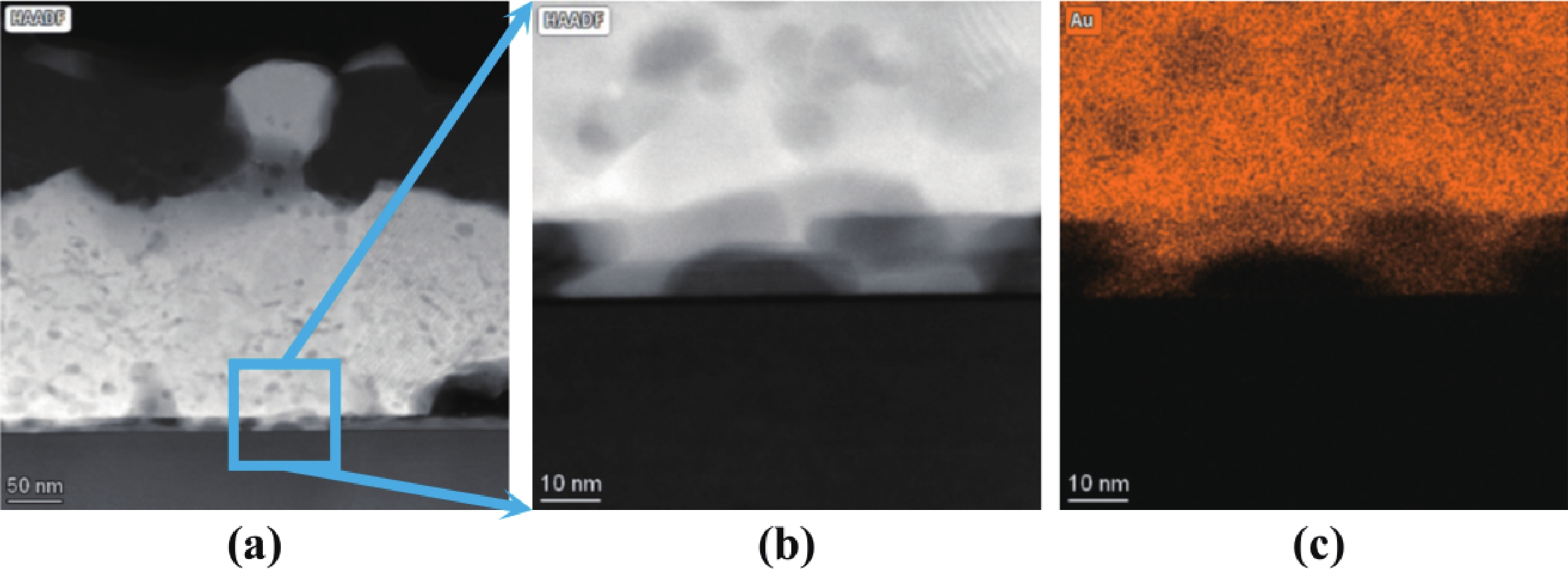
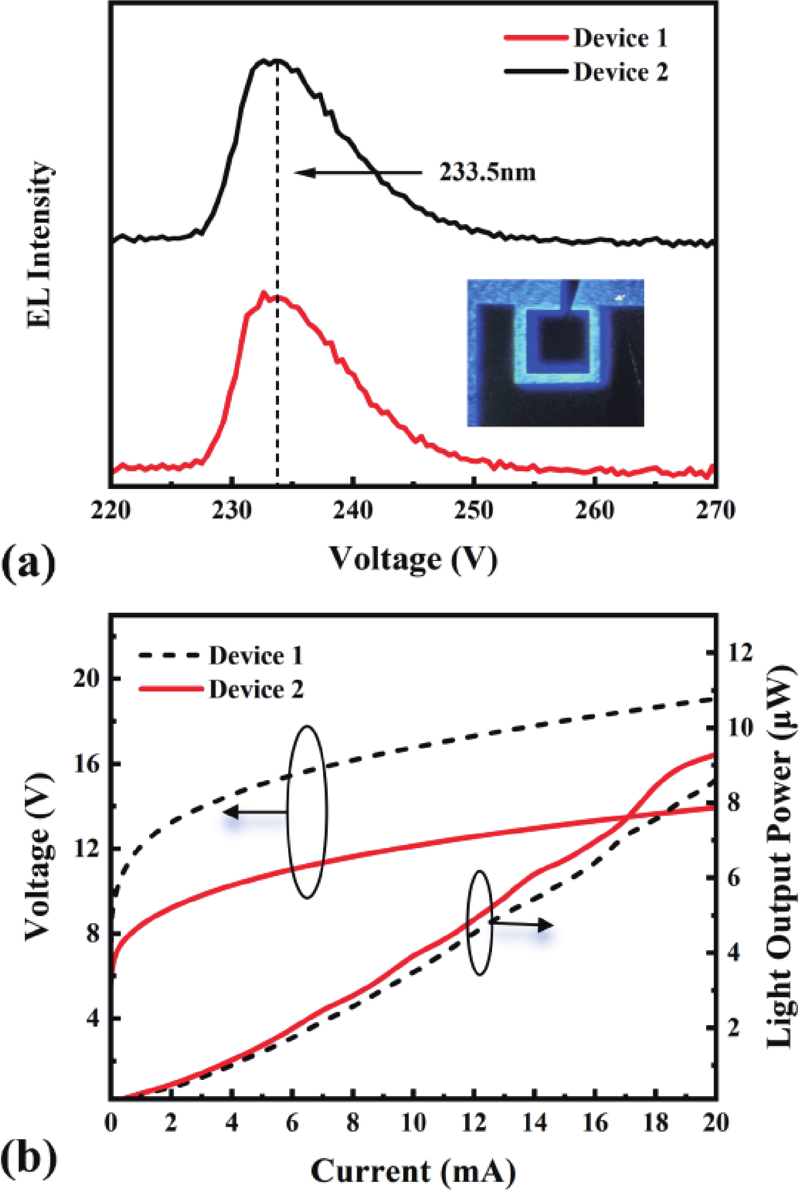
Table 1. The metal thickness in the n-electrodes for the samples A to E.
| Sample | Metal thickness (nm) | |||
| V | Al | Ti | Au | |
| A | 20 | 80 | 40 | 50 |
| B | 15 | 80 | 40 | 50 |
| C | 10 | 80 | 40 | 50 |
| D | 10 | 160 | 40 | 50 |
| E | 10 | 240 | 40 | 50 |
 DownLoad: CSV
Table 2. Optimal specific contact resistivity and their corresponding annealing temperature.
| Sample | Optimal annealing temperature (°C) |
Specific contact resistivity (Ω·cm2) |
| A | 800 | 1.74 × 10⁻² |
| B | 900 | 1.14 × 10⁻² |
| C | 850 | 9.98 × 10⁻³ |
| D | 850 | 2.69 × 10⁻³ |
| E | 850 | 7.30 × 10⁻⁴ |
DownLoad: CSV
| [1] |
Zollner C J, DenBaars S P, Speck J S, et al. Germicidal ultraviolet LEDs: A review of applications and semiconductor technologies. Semicond Sci Technol, 2021, 36(12), 123001 doi: 10.1088/1361-6641/ac27e7
|
| [2] |
Rauch K D, MacIsaac S A, Reid B, et al. A critical review of ultra-violet light emitting diodes as a one water disinfection technology. Water Res X, 2024, 25, 100271 doi: 10.1016/j.wroa.2024.100271
|
| [3] |
Zhang L, Fang Z B, Li J X, et al. Research progress on environmental stability of SARS-CoV-2 and influenza viruses. Front Microbiol, 2024, 15, 1463056 doi: 10.3389/fmicb.2024.1463056
|
| [4] |
Wang C X, Song X F, Shen J Y, et al. Recent advances in DNA-based nanoprobes for in vivo MiRNA imaging. Chemistry, 2024, 30(66), e202402566 doi: 10.1002/chem.202402566
|
| [5] |
Urban L, Charles F, de Miranda M R A, et al. Understanding the physiological effects of UV-C light and exploiting its agronomic potential before and after harvest. Plant Physiol Biochem, 2016, 105, 1 doi: 10.1016/j.plaphy.2016.04.004
|
| [6] |
Zwicker P, Schleusener J, Lohan S B, et al. Application of 233 nm far-UVC LEDs for eradication of MRSA and MSSA and risk assessment on skin models. Sci Rep, 2022, 12, 2587 doi: 10.1038/s41598-022-06397-z
|
| [7] |
Fukui T, Niikura T, Oda T, et al. Safety of 222 nm UVC irradiation to the surgical site in a rabbit model. Photochem Photobiol, 2022, 98(6), 1365 doi: 10.1111/php.13620
|
| [8] |
Buonanno M, Ponnaiya B, Welch D, et al. Germicidal efficacy and mammalian skin safety of 222-nm UV light. Radiat Res, 2017, 187(4), 483 doi: 10.1667/RR0010CC.1
|
| [9] |
Li J C, Gao N, Cai D J, et al. Multiple fields manipulation on nitride material structures in ultraviolet light-emitting diodes. Light Sci Appl, 2021, 10, 129 doi: 10.1038/s41377-021-00563-0
|
| [10] |
Moe C G, Sugiyama S, Kasai J, et al. AlGaN light-emitting diodes on AlN substrates emitting at 230 nm. Phys Status Solidi A, 2018, 215(10), 1700660 doi: 10.1002/pssa.201700660
|
| [11] |
Cai Q, You H F, Guo H, et al. Progress on AlGaN-based solar-blind ultraviolet photodetectors and focal plane arrays. Light Sci Appl, 2021, 10(1), 94 doi: 10.1038/s41377-021-00527-4
|
| [12] |
Pandey A, Gim J, Hovden R, et al. Electron overflow of AlGaN deep ultraviolet light emitting diodes. Appl Phys Lett, 2021, 118(24), 241109 doi: 10.1063/5.0055326
|
| [13] |
Mehnke F, Kuhn C, Guttmann M, et al. Efficient charge carrier injection into sub-250 nm AlGaN multiple quantum well light emitting diodes. Appl Phys Lett, 2014, 105(5), 051113 doi: 10.1063/1.4892883
|
| [14] |
Hiroki M, Taniyasu Y, Kumakura K. High-temperature performance of AlN MESFETs with epitaxially grown n-type AlN channel layers. IEEE Electron Device Lett, 2022, 43(3), 350 doi: 10.1109/LED.2022.3141100
|
| [15] |
Ebata K, Nishinaka J, Taniyasu Y, et al. High hole concentration in Mg-doped AlN/AlGaN superlattices with high Al content. Jpn J Appl Phys, 2018, 57(4S), 04FH09 doi: 10.7567/JJAP.57.04FH09
|
| [16] |
Wang J M, Wang M X, Xu F J, et al. Sub-nanometer ultrathin epitaxy of AlGaN and its application in efficient doping. Light Sci Appl, 2022, 11(1), 71 doi: 10.1038/s41377-022-00753-4
|
| [17] |
Jiang K, Sun X J, Shi Z M, et al. Quantum engineering of non-equilibrium efficient p-doping in ultra-wide band-gap nitrides. Light Sci Appl, 2021, 10(1), 69 doi: 10.1038/s41377-021-00503-y
|
| [18] |
Zhang C Y, Jiang K, Sun X J, et al. Recent progress on AlGaN based deep ultraviolet light-emitting diodes below 250 nm. Crystals, 2022, 12(12), 1812 doi: 10.3390/cryst12121812
|
| [19] |
Mehnke F, Sulmoni L, Guttmann M, et al. Influence of light absorption on the performance characteristics of UV LEDs with emission between 239 and 217 nm. Appl Phys Express, 2019, 12(1), 012008 doi: 10.7567/1882-0786/aaf788
|
| [20] |
France R, Xu T, Chen P P, et al. Vanadium-based Ohmic contacts to n-AlGaN in the entire alloy composition. Appl Phys Lett, 2007, 90(6), 062115 doi: 10.1063/1.2458399
|
| [21] |
Patsalas P, Kalfagiannis N, Kassavetis S, et al. Conductive nitrides: Growth principles, optical and electronic properties, and their perspectives in photonics and plasmonics. Mater Sci Eng R Rep, 2018, 123, 1 doi: 10.1016/j.mser.2017.11.001
|
| [22] |
Wu C I, Kahn A. Electronic states at aluminum nitride (0001)-1 × 1 surfaces. Appl Phys Lett, 1999, 74(4), 546 doi: 10.1063/1.123140
|
| [23] |
Kozawa T, Mori T, Ohwaki T, et al. UV photoemission study of AlGaN grown by metalorganic vapor phase epitaxy. Jpn J Appl Phys, 2000, 39(8A), L772 doi: 10.1143/JJAP.39.L772
|
| [24] |
Grabowski S P, Schneider M, Nienhaus H, et al. Electron affinity of AlxGa1–xN(0001) surfaces. Appl Phys Lett, 2001, 78(17), 2503 doi: 10.1063/1.1367275
|
| [25] |
Ye M Y, Hao X R, Zeng J F, et al. Research progress of alkaline earth metal iron-based oxides as anodes for lithium-ion batteries. J Semicond, 2024, 45(2), 021801 doi: 10.1088/1674-4926/45/2/021801
|
| [26] |
Kataoka K, Narita T, Yagi Y, et al. Comprehensive study of electron conduction and its compensation for degenerate Si-doped AlN-rich AlGaN. Physica Rapid Research Ltrs, 2024, 18(2), 2300055 doi: 10.1002/pssr.202300055
|
| [27] |
Mehnke F, Wernicke T, Pingel H, et al. Highly conductive n-AlxGa1–xN layers with aluminum mole fractions above 80%. Appl Phys Lett, 2013, 103(21), 212109 doi: 10.1063/1.4833247
|
| [28] |
Collazo R, Mita S, Xie J Q, et al. Progress on n-type doping of AlGaN alloys on AlN single crystal substrates for UV optoelectronic applications. Phys Status Solidi C, 2011, 8(7/8), 2031 doi: 10.1002/pssc.201000964
|
| [29] |
Moses P G, Miao M S, Yan Q M, et al. Hybrid functional investigations of band gaps and band alignments for AlN, GaN, InN, and InGaN. J Chem Phys, 2011, 134(8), 084703 doi: 10.1063/1.3548872
|
| [30] |
Yang Y, Xiong F B, Lin H Y, et al. Evaluation of Ti/Al/Ni/Au ohmic contact to n-AlGaN with different Ti/Al thickness for deep ultraviolet light emitting diode. Solid State Electron, 2023, 208, 108752 doi: 10.1016/j.sse.2023.108752
|
| [31] |
Zhao X Y, Sun K, Lv Z X, et al. Contact engineering of III-nitrides and metal schemes toward efficient deep-ultraviolet light-emitting diodes. ACS Appl Mater Interfaces, 2024, 16(5), 6605 doi: 10.1021/acsami.3c15303
|
| [32] |
Wang L, Mohammed F M, Adesida I. Differences in the reaction kinetics and contact formation mechanisms of annealed Ti∕Al/Mo/Au Ohmic contacts on n-GaN and AlGaN∕GaN epilayers. J Appl Phys, 2007, 101(1), 013702 doi: 10.1063/1.2402791
|
| [33] |
Van Daele B, Van Tendeloo G, Ruythooren W, et al. The role of Al on Ohmic contact formation on n-type GaN and AlGaN∕GaN. Appl Phys Lett, 2005, 87(6), 061905 doi: 10.1063/1.2008361
|
| [34] |
Miller M A, Koo B H, Bogart K H A, et al. Ti/Al/Ti/Au and V/Al/V/Au contacts to plasma-etched n-Al0.58Ga0.42N. J Electron Mater, 2008, 37(5), 564 doi: 10.1007/s11664-007-0300-8
|
| [35] |
Wang L, Mohammed F M, Adesida I. Formation mechanism of ohmic contacts on AlGaN/GaN heterostructure: Electrical and microstructural characterizations. J Appl Phys, 2008, 103(9), 093516 doi: 10.1063/1.2903482
|
| [36] |
Ebata K, Hiroki M, Tateno K, et al. Effects of thermal annealing on V-based ohmic contacts on n-type AlGaN with high Al content. Phys Status Solidi A, 2024, 221(21), 2400148 doi: 10.1002/pssa.202400148
|
| [37] |
Guo X Q, Xu F J, Lang J, et al. Influence of the barrier layer on the electrical properties of the V/Al-based Ohmic contact on n-type high-Al-fraction AlGaN. Appl Phys Lett, 2024, 124(23), 232106 doi: 10.1063/5.0208669
|
| [38] |
Sulmoni L, Mehnke F, Mogilatenko A, et al. Electrical properties and microstructure formation of V/Al-based n-contacts on high Al mole fraction n-AlGaN layers. Photon Res, 2020, 8(8), 1381 doi: 10.1364/PRJ.391075
|
| [39] |
Cho H K, Rass J, Mogilatenko A, et al. Impact of plasma treatment of n-Al0.87Ga0.13N: Si surfaces on V/Al/Ni/Au contacts in far-UVC LEDs. IEEE Photonics Technol Lett, 2023, 35(17), 915 doi: 10.1109/LPT.2023.3288216
|
| [40] |
Srivastava S, Hwang S M, Islam M, et al. Ohmic contact to high-aluminum-content AlGaN epilayers. J Electron Mater, 2009, 38(11), 2348 doi: 10.1007/s11664-009-0924-y
|
| [41] |
Jung S M, Lee C T, Shin M W. Investigation of V-Ti/Al/Ni/Au Ohmic contact to AlGaN/GaN heterostructures with a thin GaN cap layer. Semicond Sci Technol, 2015, 30(7), 075012 doi: 10.1088/0268-1242/30/7/075012
|
| [42] |
Schmid A, Schroeter C, Otto R, et al. Microstructure of V-based ohmic contacts to AlGaN/GaN heterostructures at a reduced annealing temperature. Appl Phys Lett, 2015, 106(5), 053509 doi: 10.1063/1.4907735
|


Article views: 1291 Times PDF downloads: 187 Times Cited by: 0 Times
Received: 21 January 2025 Revised: 22 February 2025 Online: Accepted Manuscript: 31 March 2025Uncorrected proof: 19 May 2025Published: 15 September 2025
| Citation: |
Jiale Peng, Ke Jiang, Shanli Zhang, Jianwei Ben, Kexi Liu, Ziyue Qin, Ruihua Chen, Chunyue Zhang, Shunpeng Lv, Xiaojuan Sun, Dabing Li. Reducing specific contact resistivity of V/Al/Ti/Au n-electrode on n-AlGaN with Al content over 80% for far-UVC LEDs[J]. Journal of Semiconductors, 2025, 46(9): 092501. doi: 10.1088/1674-4926/25010026
****
J L Peng, K Jiang, S L Zhang, J W Ben, K X Liu, Z Y Qin, R H Chen, C Y Zhang, S P Lv, X J Sun, and D B Li, Reducing specific contact resistivity of V/Al/Ti/Au n-electrode on n-AlGaN with Al content over 80% for far-UVC LEDs[J]. J. Semicond., 2025, 46(9), 092501 doi: 10.1088/1674-4926/25010026

|
 Jiale Peng got his bachelor’s degree in 2022 from SouthWest Petroleum University. Now he is a Master student at Changchun Institute of Optics, Fine Mechanics and Physics, Chinese Academy of Sciences, under the supervision of Prof. Dabing Li and Prof. Ke Jiang. His research focuses on the n-type AlGaN with high Al content for far-UVC LED
 Ke Jiang received his Bachelor’s degree from Xiamen University in 2014 and doctoral degree from Changchun Institute of Optics, Fine Mechanics and Physics (CIOMP), Chinese Academy of Sciences in 2019. He is currently a Professor with CIOMP, Chinese Academy of Sciences. His research interests include the growth of AlN-based materials and the opto-electronic devices
 Shanli Zhang received her Bachelor's degree and Master’s degree from Changchun University of Science and Technology in 2007 and 2010, respectively. Now, she is an engineer at Changchun Institute of Optics, Fine Mechanics and Physics, Chinese Academy of Sciences. Her research focuses on the MOCVD growth and characterization of AlN-based materials
| [1] |
Zollner C J, DenBaars S P, Speck J S, et al. Germicidal ultraviolet LEDs: A review of applications and semiconductor technologies. Semicond Sci Technol, 2021, 36(12), 123001 doi: 10.1088/1361-6641/ac27e7
|
| [2] |
Rauch K D, MacIsaac S A, Reid B, et al. A critical review of ultra-violet light emitting diodes as a one water disinfection technology. Water Res X, 2024, 25, 100271 doi: 10.1016/j.wroa.2024.100271
|
| [3] |
Zhang L, Fang Z B, Li J X, et al. Research progress on environmental stability of SARS-CoV-2 and influenza viruses. Front Microbiol, 2024, 15, 1463056 doi: 10.3389/fmicb.2024.1463056
|
| [4] |
Wang C X, Song X F, Shen J Y, et al. Recent advances in DNA-based nanoprobes for in vivo MiRNA imaging. Chemistry, 2024, 30(66), e202402566 doi: 10.1002/chem.202402566
|
| [5] |
Urban L, Charles F, de Miranda M R A, et al. Understanding the physiological effects of UV-C light and exploiting its agronomic potential before and after harvest. Plant Physiol Biochem, 2016, 105, 1 doi: 10.1016/j.plaphy.2016.04.004
|
| [6] |
Zwicker P, Schleusener J, Lohan S B, et al. Application of 233 nm far-UVC LEDs for eradication of MRSA and MSSA and risk assessment on skin models. Sci Rep, 2022, 12, 2587 doi: 10.1038/s41598-022-06397-z
|
| [7] |
Fukui T, Niikura T, Oda T, et al. Safety of 222 nm UVC irradiation to the surgical site in a rabbit model. Photochem Photobiol, 2022, 98(6), 1365 doi: 10.1111/php.13620
|
| [8] |
Buonanno M, Ponnaiya B, Welch D, et al. Germicidal efficacy and mammalian skin safety of 222-nm UV light. Radiat Res, 2017, 187(4), 483 doi: 10.1667/RR0010CC.1
|
| [9] |
Li J C, Gao N, Cai D J, et al. Multiple fields manipulation on nitride material structures in ultraviolet light-emitting diodes. Light Sci Appl, 2021, 10, 129 doi: 10.1038/s41377-021-00563-0
|
| [10] |
Moe C G, Sugiyama S, Kasai J, et al. AlGaN light-emitting diodes on AlN substrates emitting at 230 nm. Phys Status Solidi A, 2018, 215(10), 1700660 doi: 10.1002/pssa.201700660
|
| [11] |
Cai Q, You H F, Guo H, et al. Progress on AlGaN-based solar-blind ultraviolet photodetectors and focal plane arrays. Light Sci Appl, 2021, 10(1), 94 doi: 10.1038/s41377-021-00527-4
|
| [12] |
Pandey A, Gim J, Hovden R, et al. Electron overflow of AlGaN deep ultraviolet light emitting diodes. Appl Phys Lett, 2021, 118(24), 241109 doi: 10.1063/5.0055326
|
| [13] |
Mehnke F, Kuhn C, Guttmann M, et al. Efficient charge carrier injection into sub-250 nm AlGaN multiple quantum well light emitting diodes. Appl Phys Lett, 2014, 105(5), 051113 doi: 10.1063/1.4892883
|
| [14] |
Hiroki M, Taniyasu Y, Kumakura K. High-temperature performance of AlN MESFETs with epitaxially grown n-type AlN channel layers. IEEE Electron Device Lett, 2022, 43(3), 350 doi: 10.1109/LED.2022.3141100
|
| [15] |
Ebata K, Nishinaka J, Taniyasu Y, et al. High hole concentration in Mg-doped AlN/AlGaN superlattices with high Al content. Jpn J Appl Phys, 2018, 57(4S), 04FH09 doi: 10.7567/JJAP.57.04FH09
|
| [16] |
Wang J M, Wang M X, Xu F J, et al. Sub-nanometer ultrathin epitaxy of AlGaN and its application in efficient doping. Light Sci Appl, 2022, 11(1), 71 doi: 10.1038/s41377-022-00753-4
|
| [17] |
Jiang K, Sun X J, Shi Z M, et al. Quantum engineering of non-equilibrium efficient p-doping in ultra-wide band-gap nitrides. Light Sci Appl, 2021, 10(1), 69 doi: 10.1038/s41377-021-00503-y
|
| [18] |
Zhang C Y, Jiang K, Sun X J, et al. Recent progress on AlGaN based deep ultraviolet light-emitting diodes below 250 nm. Crystals, 2022, 12(12), 1812 doi: 10.3390/cryst12121812
|
| [19] |
Mehnke F, Sulmoni L, Guttmann M, et al. Influence of light absorption on the performance characteristics of UV LEDs with emission between 239 and 217 nm. Appl Phys Express, 2019, 12(1), 012008 doi: 10.7567/1882-0786/aaf788
|
| [20] |
France R, Xu T, Chen P P, et al. Vanadium-based Ohmic contacts to n-AlGaN in the entire alloy composition. Appl Phys Lett, 2007, 90(6), 062115 doi: 10.1063/1.2458399
|
| [21] |
Patsalas P, Kalfagiannis N, Kassavetis S, et al. Conductive nitrides: Growth principles, optical and electronic properties, and their perspectives in photonics and plasmonics. Mater Sci Eng R Rep, 2018, 123, 1 doi: 10.1016/j.mser.2017.11.001
|
| [22] |
Wu C I, Kahn A. Electronic states at aluminum nitride (0001)-1 × 1 surfaces. Appl Phys Lett, 1999, 74(4), 546 doi: 10.1063/1.123140
|
| [23] |
Kozawa T, Mori T, Ohwaki T, et al. UV photoemission study of AlGaN grown by metalorganic vapor phase epitaxy. Jpn J Appl Phys, 2000, 39(8A), L772 doi: 10.1143/JJAP.39.L772
|
| [24] |
Grabowski S P, Schneider M, Nienhaus H, et al. Electron affinity of AlxGa1–xN(0001) surfaces. Appl Phys Lett, 2001, 78(17), 2503 doi: 10.1063/1.1367275
|
| [25] |
Ye M Y, Hao X R, Zeng J F, et al. Research progress of alkaline earth metal iron-based oxides as anodes for lithium-ion batteries. J Semicond, 2024, 45(2), 021801 doi: 10.1088/1674-4926/45/2/021801
|
| [26] |
Kataoka K, Narita T, Yagi Y, et al. Comprehensive study of electron conduction and its compensation for degenerate Si-doped AlN-rich AlGaN. Physica Rapid Research Ltrs, 2024, 18(2), 2300055 doi: 10.1002/pssr.202300055
|
| [27] |
Mehnke F, Wernicke T, Pingel H, et al. Highly conductive n-AlxGa1–xN layers with aluminum mole fractions above 80%. Appl Phys Lett, 2013, 103(21), 212109 doi: 10.1063/1.4833247
|
| [28] |
Collazo R, Mita S, Xie J Q, et al. Progress on n-type doping of AlGaN alloys on AlN single crystal substrates for UV optoelectronic applications. Phys Status Solidi C, 2011, 8(7/8), 2031 doi: 10.1002/pssc.201000964
|
| [29] |
Moses P G, Miao M S, Yan Q M, et al. Hybrid functional investigations of band gaps and band alignments for AlN, GaN, InN, and InGaN. J Chem Phys, 2011, 134(8), 084703 doi: 10.1063/1.3548872
|
| [30] |
Yang Y, Xiong F B, Lin H Y, et al. Evaluation of Ti/Al/Ni/Au ohmic contact to n-AlGaN with different Ti/Al thickness for deep ultraviolet light emitting diode. Solid State Electron, 2023, 208, 108752 doi: 10.1016/j.sse.2023.108752
|
| [31] |
Zhao X Y, Sun K, Lv Z X, et al. Contact engineering of III-nitrides and metal schemes toward efficient deep-ultraviolet light-emitting diodes. ACS Appl Mater Interfaces, 2024, 16(5), 6605 doi: 10.1021/acsami.3c15303
|
| [32] |
Wang L, Mohammed F M, Adesida I. Differences in the reaction kinetics and contact formation mechanisms of annealed Ti∕Al/Mo/Au Ohmic contacts on n-GaN and AlGaN∕GaN epilayers. J Appl Phys, 2007, 101(1), 013702 doi: 10.1063/1.2402791
|
| [33] |
Van Daele B, Van Tendeloo G, Ruythooren W, et al. The role of Al on Ohmic contact formation on n-type GaN and AlGaN∕GaN. Appl Phys Lett, 2005, 87(6), 061905 doi: 10.1063/1.2008361
|
| [34] |
Miller M A, Koo B H, Bogart K H A, et al. Ti/Al/Ti/Au and V/Al/V/Au contacts to plasma-etched n-Al0.58Ga0.42N. J Electron Mater, 2008, 37(5), 564 doi: 10.1007/s11664-007-0300-8
|
| [35] |
Wang L, Mohammed F M, Adesida I. Formation mechanism of ohmic contacts on AlGaN/GaN heterostructure: Electrical and microstructural characterizations. J Appl Phys, 2008, 103(9), 093516 doi: 10.1063/1.2903482
|
| [36] |
Ebata K, Hiroki M, Tateno K, et al. Effects of thermal annealing on V-based ohmic contacts on n-type AlGaN with high Al content. Phys Status Solidi A, 2024, 221(21), 2400148 doi: 10.1002/pssa.202400148
|
| [37] |
Guo X Q, Xu F J, Lang J, et al. Influence of the barrier layer on the electrical properties of the V/Al-based Ohmic contact on n-type high-Al-fraction AlGaN. Appl Phys Lett, 2024, 124(23), 232106 doi: 10.1063/5.0208669
|
| [38] |
Sulmoni L, Mehnke F, Mogilatenko A, et al. Electrical properties and microstructure formation of V/Al-based n-contacts on high Al mole fraction n-AlGaN layers. Photon Res, 2020, 8(8), 1381 doi: 10.1364/PRJ.391075
|
| [39] |
Cho H K, Rass J, Mogilatenko A, et al. Impact of plasma treatment of n-Al0.87Ga0.13N: Si surfaces on V/Al/Ni/Au contacts in far-UVC LEDs. IEEE Photonics Technol Lett, 2023, 35(17), 915 doi: 10.1109/LPT.2023.3288216
|
| [40] |
Srivastava S, Hwang S M, Islam M, et al. Ohmic contact to high-aluminum-content AlGaN epilayers. J Electron Mater, 2009, 38(11), 2348 doi: 10.1007/s11664-009-0924-y
|
| [41] |
Jung S M, Lee C T, Shin M W. Investigation of V-Ti/Al/Ni/Au Ohmic contact to AlGaN/GaN heterostructures with a thin GaN cap layer. Semicond Sci Technol, 2015, 30(7), 075012 doi: 10.1088/0268-1242/30/7/075012
|
| [42] |
Schmid A, Schroeter C, Otto R, et al. Microstructure of V-based ohmic contacts to AlGaN/GaN heterostructures at a reduced annealing temperature. Appl Phys Lett, 2015, 106(5), 053509 doi: 10.1063/1.4907735
|
 Supplementary_information.pdf
|

|

 WeChat ID
Journal of Semiconductors © 2017 All Rights Reserved 京ICP备05085259号-2


