| [1] |
Wang Z W, Nayak P K, Caraveo-Frescas J A, et al. Recent developments in p-type oxide semiconductor materials and devices. Adv Mater, 2016, 28(20), 3831 doi: 10.1002/adma.201503080 |
| [2] |
Jeong H, Kong C S, Chang S W, et al. Temperature sensor made of amorphous indium–gallium–zinc oxide TFTs. IEEE Electron Device Lett, 2013, 34(12), 1569 doi: 10.1109/LED.2013.2286824 |
| [3] |
Hung M H, Chen C H, Lai Y C, et al. Ultra low voltage 1-V RFID tag implement in a-IGZO TFT technology on plastic. 2017 IEEE International Conference on RFID (RFID), 2017, 193 doi: 10.1109/RFID.2017.7945608 |
| [4] |
Zhang W, Liang R R, Liu L B, et al. Demonstration of α-InGaZnO TFT nonvolatile memory using TiAlO charge trapping layer. IEEE Trans Nanotechnol, 2018, 17(6), 1089 doi: 10.1109/TNANO.2018.2810885 |
| [5] |
Shiah Y S, Sim K, Shi Y H, et al. Mobility–stability trade-off in oxide thin-film transistors. Nat Electron, 2021, 4, 800 doi: 10.1038/s41928-021-00671-0 |
| [6] |
Nomura K, Kamiya T, Hosono H. Ambipolar oxide thin-film transistor. Adv Mater, 2011, 23(30), 3431 doi: 10.1002/adma.201101410 |
| [7] |
Caraveo-Frescas J A, Nayak P K, Al-Jawhari H A, et al. Record mobility in transparent p-type tin monoxide films and devices by phase engineering. ACS Nano, 2013, 7(6), 5160 doi: 10.1021/nn400852r |
| [8] |
Hu Y Q, Yao X L, Schlom D G, et al. First principles design of high hole mobility p-type Sn−O− X ternary oxides: Valence orbital engineering of Sn 2+ in Sn 2+−O− X by selection of appropriate elements X. Chem Mater, 2021, 33(1), 212 doi: 10.1021/acs.chemmater.0c03495 |
| [9] |
Hsu S M, Yang C E, Lu M H, et al. Mobility enhancement in P-type SnO thin-film transistors via Ni incorporation by co-sputtering. IEEE Electron Device Lett, 2022, 43(2), 228 doi: 10.1109/LED.2021.3136966 |
| [10] |
Qin L, Yuan S G, Chen Z Q, et al. Solution-processed transparent p-type orthorhombic K doped SnO films and their application in a phototransistor. Nanoscale, 2022, 14(37), 13763 doi: 10.1039/D2NR03785H |
| [11] |
Zhang Z F, Guo Y Z, Robertson J. P-type semiconduction in oxides with cation lone pairs. Chem Mater, 2022, 34(2), 643 doi: 10.1021/acs.chemmater.1c03323 |
| [12] |
Hu Y Q, Hwang J, Lee Y, et al. First principles calculations of intrinsic mobilities in tin-based oxide semiconductors SnO, SnO 2, and Ta 2SnO 6. J Appl Phys, 2019, 126(18), 185701 doi: 10.1063/1.5109265 |
| [13] |
Hu Y Q, Schlom D, Datta S, et al. Amorphous Ta 2SnO 6: A hole-dopable p-type oxide. Appl Surf Sci, 2023, 613, 155981 doi: 10.1016/j.apsusc.2022.155981 |
| [14] |
Barone M, Foody M, Hu Y Q, et al. Growth of Ta 2SnO 6 films, a candidate wide-band-gap p-type oxide. J Phys Chem C, 2022, 126(7), 3764 doi: 10.1021/acs.jpcc.1c10382 |
| [15] |
Huang A P, Chu P K. Crystallization improvement of Ta 2O 5 thin films by the addition of water vapor. J Cryst Growth, 2005, 274(1/2), 73 doi: 10.1016/j.jcrysgro.2004.10.004 |
| [16] |
Huang A P, Xu S L, Zhu M K, et al. Crystallization control of sputtered Ta 2O 5 thin films by substrate bias. Appl Phys Lett, 2003, 83(16), 3278 doi: 10.1063/1.1610247 |
| [17] |
Zhou Y Y, Song Y, Hong R H, et al. Electrical evolution of p-type SnOx film and transistor deposited by RF magnetron sputtering. IEEE Trans Electron Devices, 2023, 70(6), 3100 doi: 10.1109/TED.2023.3266417 |
| [18] |
Perron A, Politano O, Vignal V. Grain size, stress and surface roughness. Surf Interface Anal, 2008, 40(3/4), 518 doi: 10.1002/sia.2849 |
| [19] |
Ono H, Koyanagi K I. Infrared absorption peak due to Ta=O bonds in Ta 2O 5 thin films. Appl Phys Lett, 2000, 77(10), 1431 doi: 10.1063/1.1290494 |
| [20] |
Zhao Y P, Wang Z X, Xu G W, et al. High performance indium-gallium-zinc oxide thin film transistor via interface engineering. Adv Funct Mater, 2020, 30(34), 2003285 doi: 10.1002/adfm.202003285 |
| [21] |
Lee S J, Jang Y, Kim H J, et al. Composition, microstructure, and electrical performance of sputtered SnO thin films for p-type oxide semiconductor. ACS Appl Mater Interfaces, 2018, 10(4), 3810 doi: 10.1021/acsami.7b17906 |
| [22] |
Bae K H, Shin M G, Hwang S H, et al. Electrical performance and stability improvement of p-channel SnO thin-film transistors using atomic-layer-deposited Al 2O 3 capping layer. IEEE Access, 2020, 8, 222410 doi: 10.1109/ACCESS.2020.3043780 |
| [23] |
Makuła P, Pacia M, Macyk W. How to correctly determine the band gap energy of modified semiconductor photocatalysts based on UV-vis spectra. J Phys Chem Lett, 2018, 9(23), 6814 doi: 10.1021/acs.jpclett.8b02892 |
| [24] |
Qiao L S, He G, Hao L, et al. Interface optimization of passivated Er 2O 3/Al 2O 3/InP MOS capacitors and modulation of leakage current conduction mechanism. IEEE Trans Electron Devices, 2021, 68(6), 2899 doi: 10.1109/TED.2021.3072928 |
| [25] |
Yan Y Y, Kilchytska V, Flandre D, et al. Investigation and optimization of traps properties in Al 2O 3/SiO 2 dielectric stacks using conductance method. Solid State Electron, 2022, 194, 108347 doi: 10.1016/j.sse.2022.108347 |
| [26] |
Han S, Flewitt A J. The origin of the high off-state current in p-type Cu 2O thin film transistors. IEEE Electron Device Lett, 2017, 38(10), 1394 doi: 10.1109/LED.2017.2748064 |
| [27] |
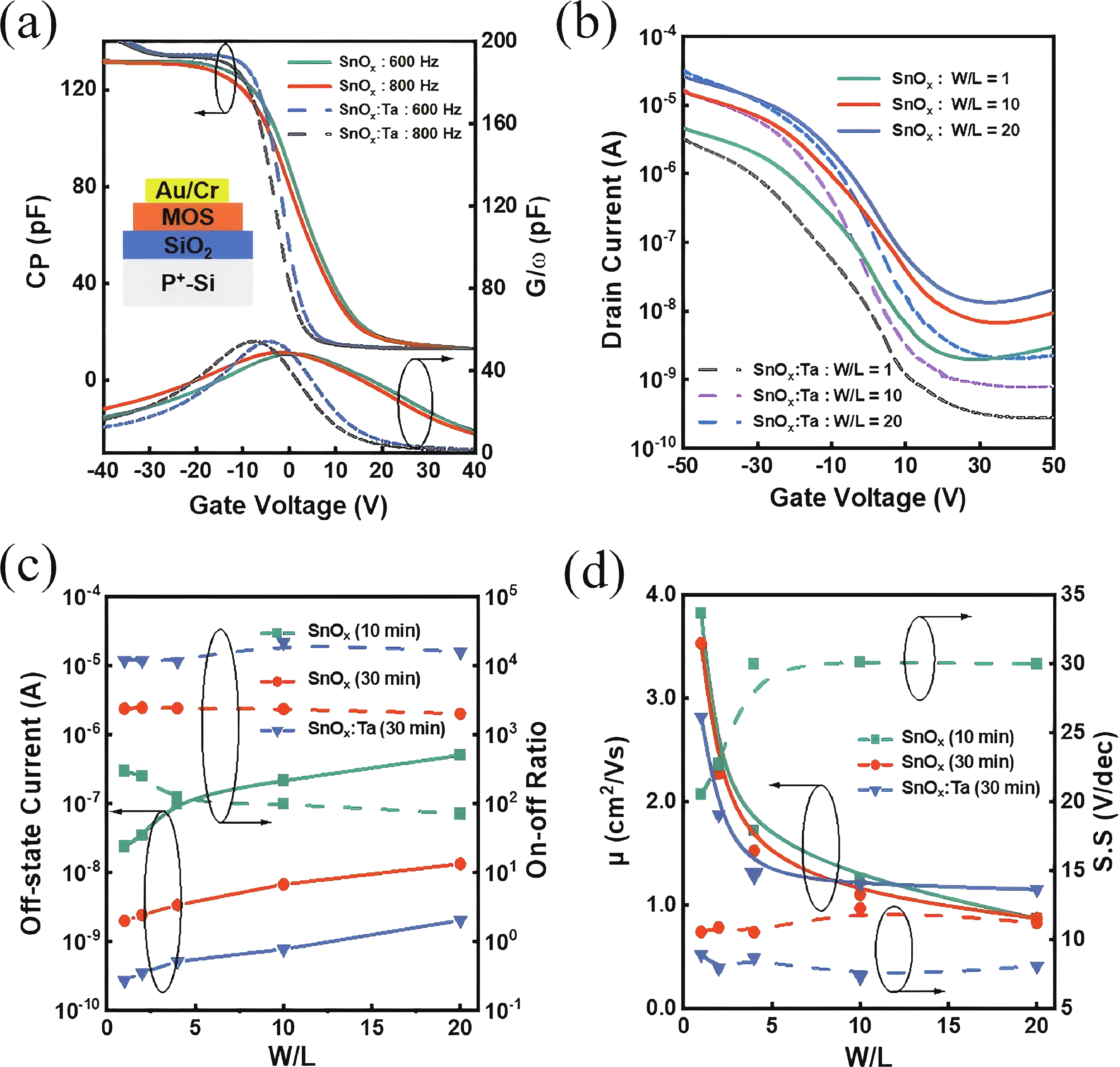
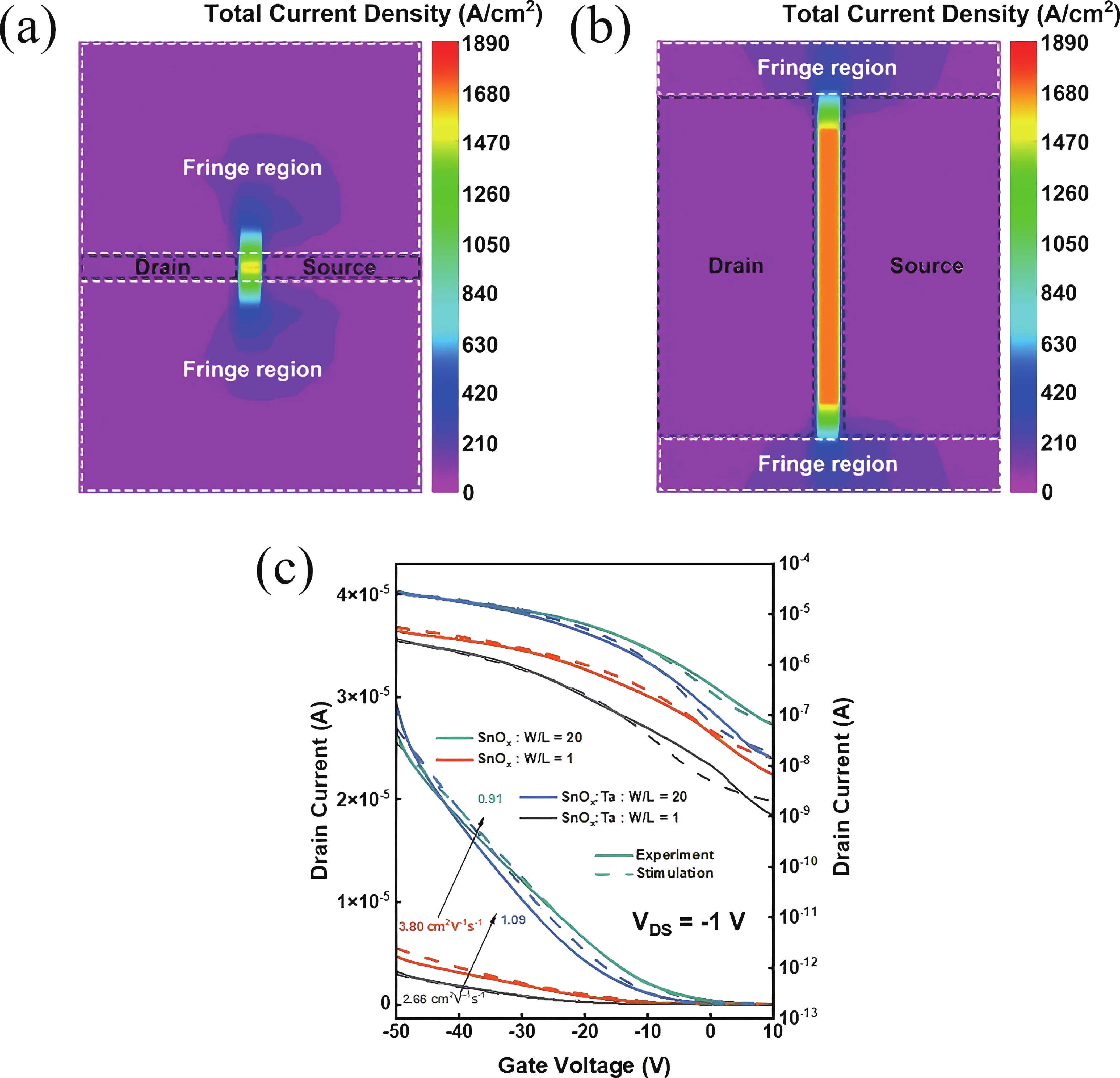
Chen C D, Chen Z H, Xu K J, et al. Thin-film transistors with the fringe effect and the correction factor for mobility extraction. IEEE Electron Device Lett, 2019, 40(6), 897 doi: 10.1109/LED.2019.2909282 |
| [28] |
Pei K, Chen M, Zhou Z W, et al. Overestimation of carrier mobility in organic thin film transistors due to unaccounted fringe currents. ACS Appl Electron Mater, 2019, 1(3), 379 doi: 10.1021/acsaelm.8b00097 |
| [29] |
Okamura K, Nikolova D, Mechau N, et al. Appropriate choice of channel ratio in thin-film transistors for the exact determination of field-effect mobility. Appl Phys Lett, 2009, 94(18), 183503 doi: 10.1063/1.3126956 |
| [30] |
Huang C H, Tang Y L, Yang T Y, et al. Atomically thin tin monoxide-based p-channel thin-film transistor and a low-power complementary inverter. ACS Appl Mater Interfaces, 2021, 13(44), 52783 doi: 10.1021/acsami.1c15990 |
| [31] |
Atlas user’s manual: device simulation software (Silvaco Inc., Santa Clara, CA, 2019
|
| [32] |
Rajshekar K, Hsu H H, Kumar K U M, et al. Effect of plasma fluorination in p-type SnO TFTs: Experiments, modeling, and simulation. IEEE Trans Electron Devices, 2019, 66(3), 1314 doi: 10.1109/TED.2019.2895042 |
| [33] |
Shi Y P, Liu G X, Wu X M, et al. UV-ozone-assisted solution-processed high-k ZrO 2 for MoS 2 field-effect transistors. IEEE Trans Electron Devices, 2024, 71(4), 2789 doi: 10.1109/TED.2024.3365459 |
| [34] |
Qu Y X, Yang J, Li Y P, et al. Organic and inorganic passivation of p-type SnO thin-film transistors with different active layer thicknesses. Semicond Sci Technol, 2018, 33(7), 075001 doi: 10.1088/1361-6641/aac3c4 |
| [35] |
Park J S, Jeong J K, Chung H J, et al. Electronic transport properties of amorphous indium-gallium-zinc oxide semiconductor upon exposure to water. Appl Phys Lett, 2008, 92(7), 072104 doi: 10.1063/1.2838380 |


 Yu Song received his BS degrees Electronic Information Engineering from Hunan University of Information Technology. Now, he is a PhD student at the School of Physics and Electronics, Hunan University under the supervision of Professor Guoli Li. His research focuses on p-type metal oxide thin film transistors.
 Guoli Li received the dual Ph.D. degrees in Electrical Engineering from Université catholique de Louvain (Belgium) and in Circuits and Systems from Hunan University in 2017. She currently serves as an associate Professor at the College of Semiconductors (College of Integrated Circuits), Hunan University. And her primary research focuses on thin-film transistors and device modeling.
 DownLoad: