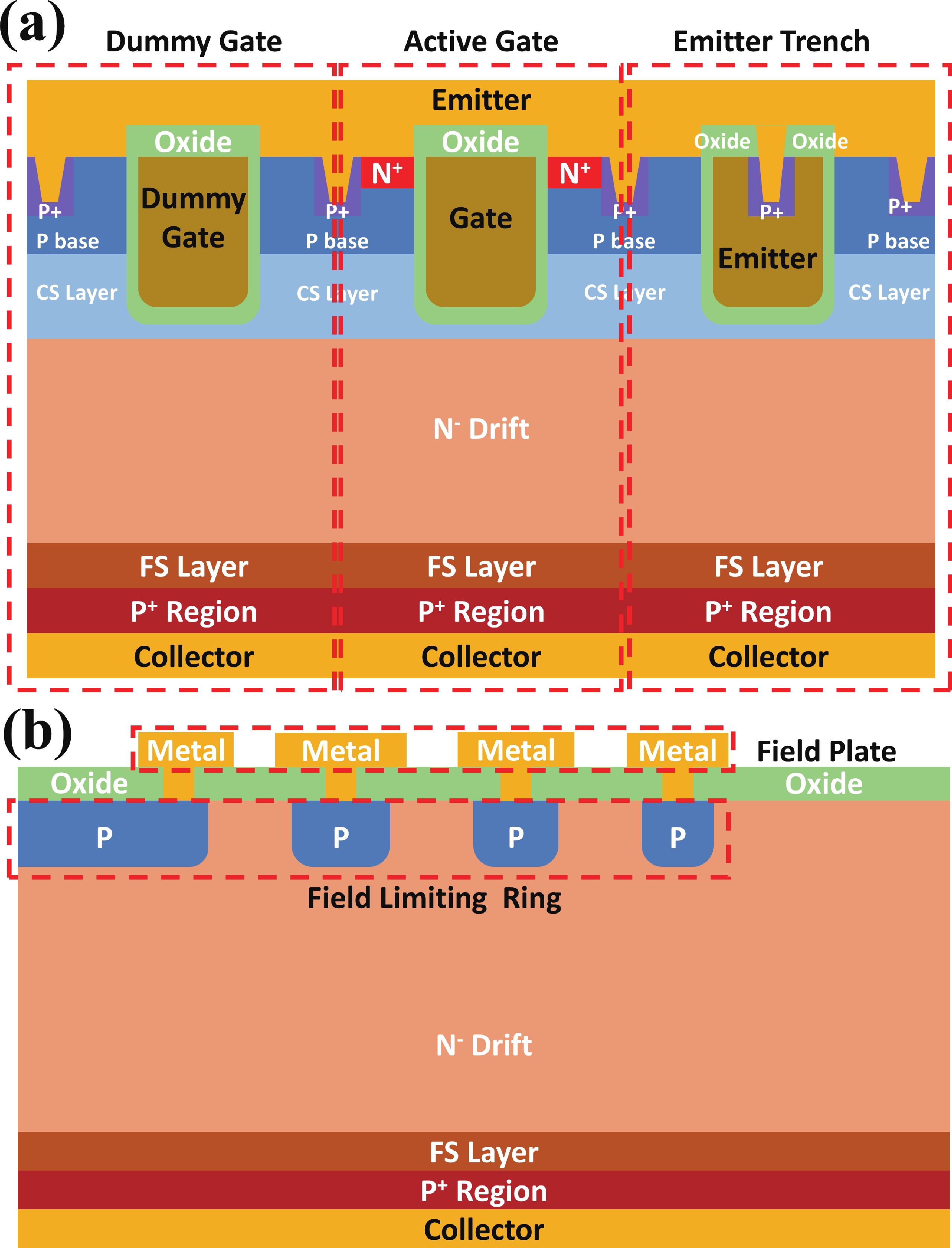
Fig. 1.
(Color online) Cross-sectional (a) cell and (b) terminal structure view of the FS-IGBT.
ARTICLES
Jingping Zhang1, Houcai Luo1, Huan Wu1, Bofeng Zheng1 and Xianping Chen1, 2,
Corresponding author: Xianping Chen, xianpingchen@cqu.edu.cn
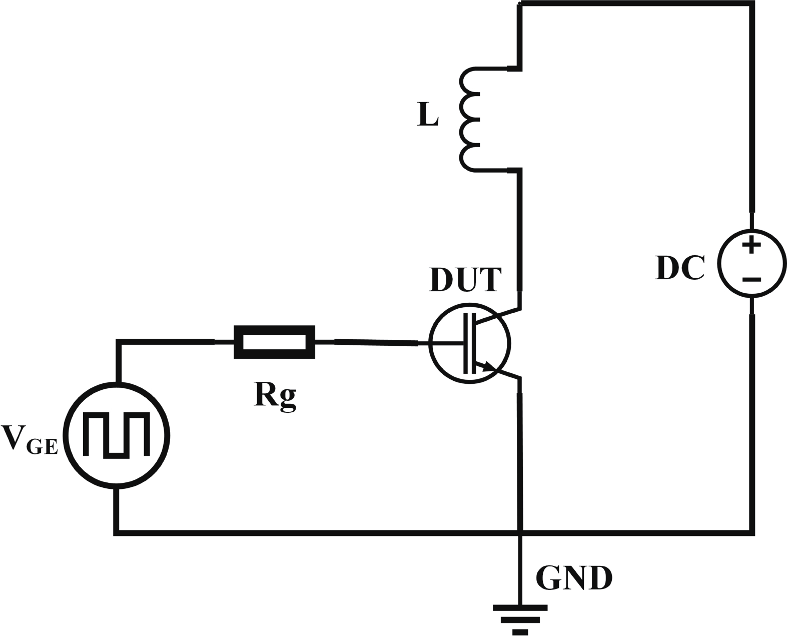
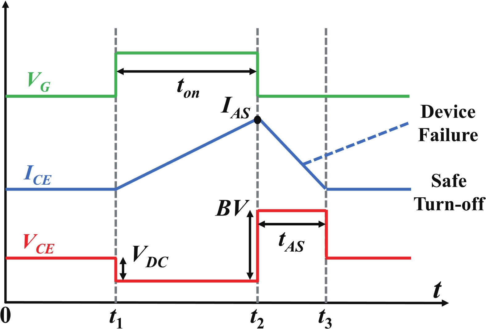
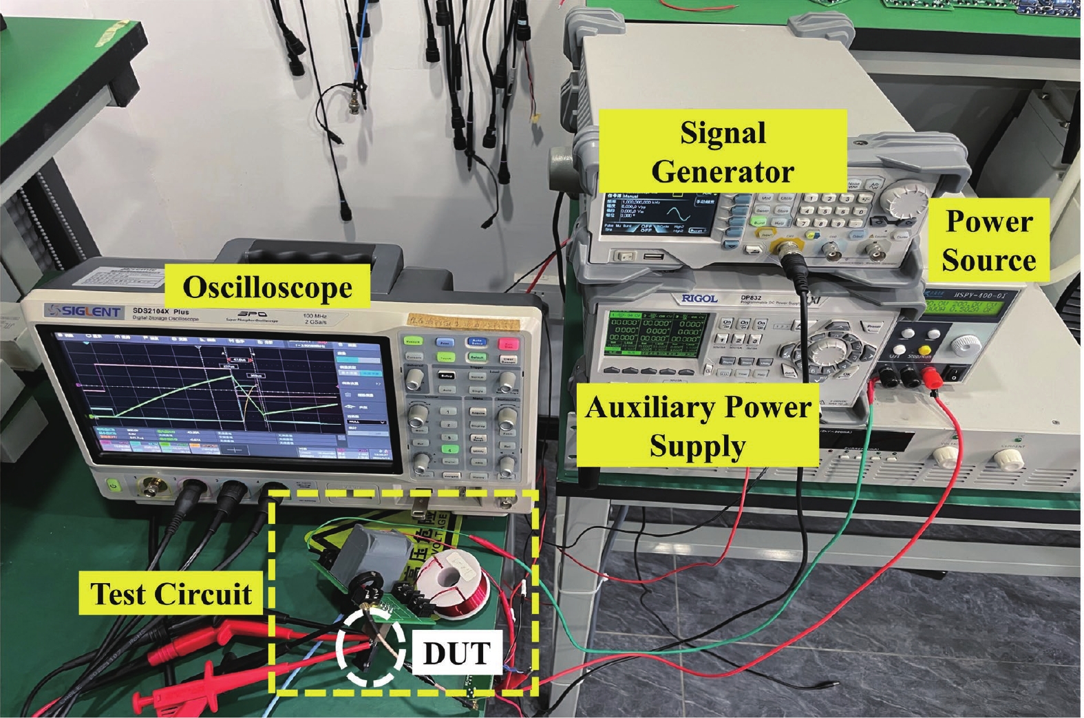
Abstract: The dynamic avalanche effect is a critical factor influencing the performance and reliability of the field-stop insulated gate bipolar transistors (FS-IGBT). Unclamped inductive switching (UIS) is the primary method for testing the dynamic avalanche capability of FS-IGBTs. Numerous studies have demonstrated that factors such as device structure, avalanche-generating current filaments, and electrical parameters influence the dynamic avalanche effect of the FS-IGBT. However, few studies have focused on enhancing the avalanche reliability of the FS-IGBT by adjusting circuit parameters during operation. In this paper, the dynamic avalanche effect of the FS-IGBT under UIS conditions is comprehensively investigated through a series of comparative experiments with varying circuit parameters, including bus voltage VDC, gate voltage VG, gate resistance Rg, load inductance L, and temperature TC. Furthermore, a method to enhance the dynamic avalanche reliability of the FS-IGBT under UIS by optimizing circuit parameters is proposed. In practical applications, reducing gate voltage, increasing load inductance, and lowering temperature can effectively improve the dynamic avalanche capability of the FS-IGBT.
Keywords: FS-IGBT, dynamic avalanche, UIS, reliability, circuit parameters
| [1] |
Breglio G, Irace A, Napoli E, et al. Study of a failure mechanism during UIS switching of planar PT-IGBT with current sense cell. Microelectron Reliab, 2007, 47(9/10/11), 1756 doi: 10.1016/j.microrel.2007.07.009
|
| [2] |
Liu S Y, Tong X, Wei J X, et al. Single-pulse avalanche failure investigations of Si-SJ-mosfet and SiC-mosfet by step-control infrared thermography method. IEEE Trans Power Electron, 2020, 35(5), 5180 doi: 10.1109/TPEL.2019.2946792
|
| [3] |
Hasegawa K, Taguchi K, Kagawa Y, et al. Which is harder SOA test for SiC MOSFET to do Unclamped Inductive Switching (UIS) or Unloaded Short Circuit mode Switching (USCS)? Does UIS play a role of USCS? 2020 32nd International Symposium on Power Semiconductor Devices and ICs (ISPSD), 2020, 62 doi: 10.1109/ISPSD46842.2020.9170172
|
| [4] |
Z H, Lin Z, Hu S D, et al. Comparative study on the short-circuit withstand capability between the superjunction and conventional field-stop IGBTs. Microelectron Reliab, 2024, 156, 115387 doi: 10.1016/j.microrel.2024.115387
|
| [5] |
Sano K, Matsushita Y, Yachi M, et al. Small current unclamped inductive switching (UIS) to detect fabrication defect for mass-production phase IGBT. 2018 IEEE 30th International Symposium on Power Semiconductor Devices and ICs (ISPSD), 2018, 116 doi: 10.1109/ISPSD.2018.8393616
|
| [6] |
Ren N, Wang K L, Wu J P, et al. Failure mechanism analysis of SiC MOSFETs in unclamped inductive switching conditions. 2019 31st International Symposium on Power Semiconductor Devices and ICs (ISPSD), 2019, 183 doi: 10.1109/ISPSD.2019.8757657
|
| [7] |
Ma X, Huang Y L, Tang X, et al. Numerical modeling of FS-trench IGBTs by TCAD and its parameter extraction method. Microelectron Reliab, 2023, 147, 115053 doi: 10.1016/j.microrel.2023.115053
|
| [8] |
Tanaka M, Nakagawa A. Simulation studies for avalanche induced short-circuit current crowding of MOSFET-Mode IGBT. 2015 IEEE 27th International Symposium on Power Semiconductor Devices & IC’s (ISPSD), 2015, 121 doi: 10.1109/ISPSD.2015.7123404
|
| [9] |
Endo K, Nagamine S, Saito W, et al. Direct photo emission motion observation of current filaments in the IGBT under avalanche breakdown condition. 2016 28th International Symposium on Power Semiconductor Devices and ICs (ISPSD), 2016, 367 doi: 10.1109/ISPSD.2016.7520854
|
| [10] |
Li L P, Li Z H, Wu Y Z, et al. Investigation on robust avalanche capacity of super-junction IGBT under UIS stress. IEEE Trans Electron Devices, 2024, 71(8), 4853 doi: 10.1109/TED.2024.3408774
|
| [11] |
Riccio M, Irace A, Breglio G, et al. Electro-thermal instability in multi-cellular Trench-IGBTs in avalanche condition: Experiments and simulations. 2011 IEEE 23rd International Symposium on Power Semiconductor Devices and ICs, 2011, 124 doi: 10.1109/ISPSD.2011.5890806
|
| [12] |
Suzuki H, Ciappa M. TCAD simulation of current filamentation in adjacent IGBT cells under turn-on and turn-off short circuit condition. Microelectron Reliab, 2015, 55(9/10), 1976 doi: 10.1016/j.microrel.2015.06.110
|
| [13] |
Shankar B, Zeng K, Gunning B, et al. Movement of current filaments and its impact on avalanche robustness in vertical GaN P-N diode under UIS stress. 2022 Device Research Conference (DRC), 2022, 1 doi: 10.1109/DRC55272.2022.9855818
|
| [14] |
Endo K, Chinone N, Nakamura T, et al. Single-pulse observation of photoemission during avalanche breakdown in insulated gate bipolar transistor. Microelectron Reliab, 2020, 114, 113739 doi: 10.1016/j.microrel.2020.113739
|
| [15] |
Breglio G, Irace A, Napoli E, et al. Detection of localized UIS failure on IGBTs with the aid of lock-in thermography. Microelectron Reliab, 2008, 48(8/9), 1432 doi: 10.1016/j.microrel.2008.06.042
|
| [16] |
Suwa T. 2D-TCAD simulation study of capture layer and repellent layer of current filament in trench-gate IGBTs. 2021 International Conference on Simulation of Semiconductor Processes and Devices (SISPAD), 2021, 32 doi: 10.1109/SISPAD54002.2021.9592570
|
| [17] |
Breglio G, Irace A, Napoli E, et al. Experimental detection and numerical validation of different failure mechanisms in IGBTs during unclamped inductive switching. IEEE Trans Electron Devices, 2013, 60(2), 563 doi: 10.1109/TED.2012.2226177
|
| [18] |
Shoji T, Ishiko M, Fukami T, et al. Investigations on current filamentation of IGBTs under undamped inductive switching conditions. Proceedings of ISPSD '05. The 17th International Symposium on Power Semiconductor Devices and ICs, 2005, 227 doi: 10.1109/ISPSD.2005.1487992
|
| [19] |
Tanaka M, Abe N, Nakagawa A. Impact of 3D simulation on the analysis of unclamped inductive switching. Jpn J Appl Phys, 2020, 59, SGGD01 doi: 10.7567/1347-4065/ab5b3a
|
| [20] |
Spirito P, Breglio G, Irace A, et al. Physics of the negative resistance in the avalanche I-V curve of field stop IGBTs: Collector design rules for improved ruggedness. IEEE Trans Electron Devices, 2014, 61(5), 1457 doi: 10.1109/TED.2014.2311169
|
| [21] |
Spirito P, Maresca L, Riccio M, et al. Effect of the collector design on the IGBT avalanche ruggedness: A comparative analysis between punch-through and field-stop devices. IEEE Trans Electron Devices, 2015, 62(8), 2535 doi: 10.1109/TED.2015.2442334
|
| [22] |
Tong X, Liu S Y, Sun W F, et al. Complete avalanche process and failure mechanism of trench-gate FS-IGBT under unclamped inductive switching by using infrared visualization method. IEEE Trans Electron Devices, 2020, 67(9), 3908 doi: 10.1109/TED.2020.3011644
|
| [23] |
Bao X K, Zhu A K, Chen R T, et al. Voltage-balanced behavioral model considering carrier extraction effect for series-connected trench gate FS-IGBTs. 2022 IEEE International Power Electronics and Application Conference and Exposition (PEAC), 2022, 566 doi: 10.1109/PEAC56338.2022.9959620
|
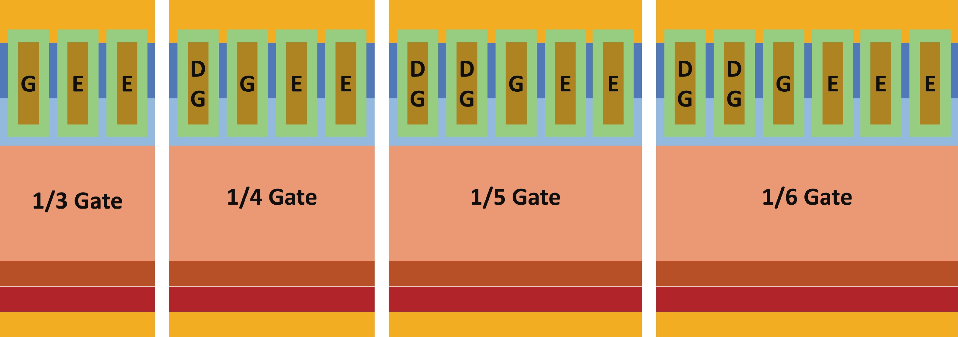
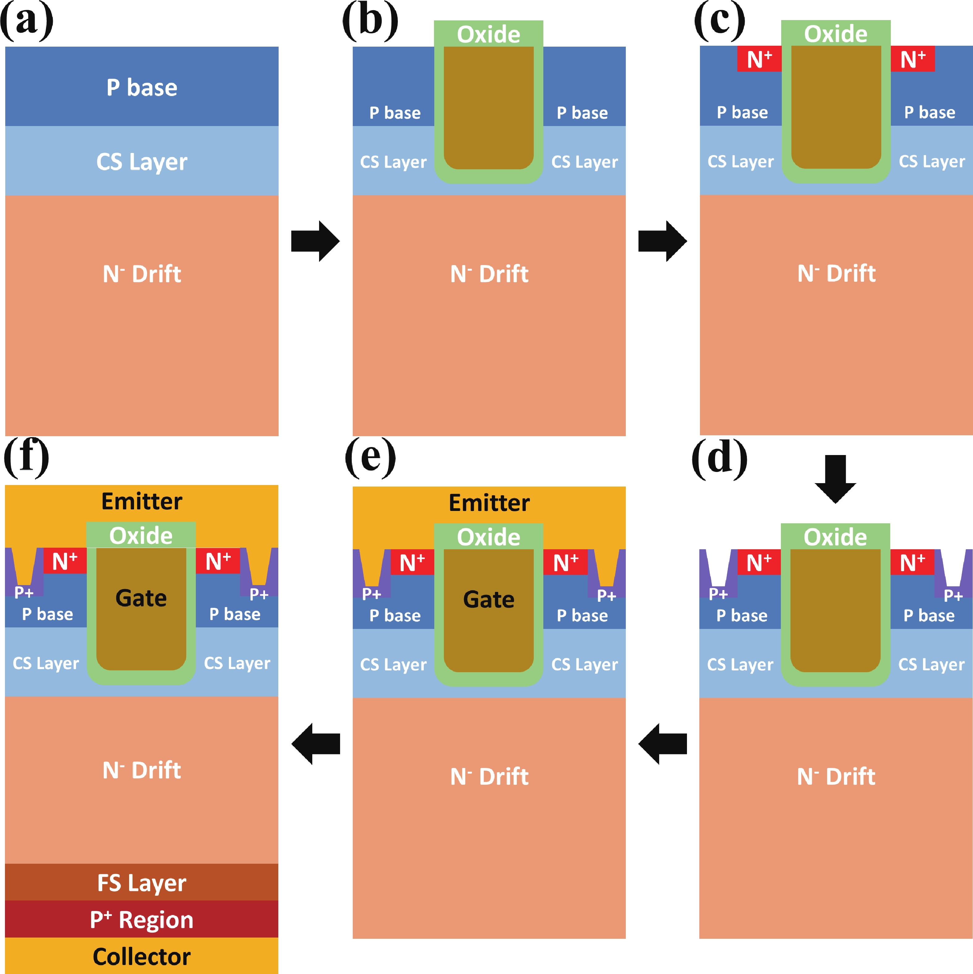
Table 1. Simulation parameters of the FS-IGBT structure.
| Symbol | Structure parameter | Value | Unit |
| TCP+ | Collector P+ region depth | 1.0 | μm |
| NCP+ | Collector P+ doping concentration | 3.0 × 10¹⁷ | cm−3 |
| TFS | FS layer depth | 2.0 | μm |
| NFS | FS layer doping concentration | 3.0 × 10¹⁶ | cm−3 |
| Td | Drift thickness | 57.0 | μm |
| Nd | Drift doping concentration | 1.0 × 10¹⁴ | cm−3 |
| Tt | Trench depth | 5.0 | μm |
| Wt | Trench width | 1.0 | μm |
| Tox | Gate oxide thickness | 0.12 | μm |
| TCS | Carrier storage (CS) layer depth | 2.5 | μm |
| NCS | CS layer doping concentration | 3.0 × 10¹⁵ | cm−3 |
| TPbase | P base depth | 3.0 | μm |
| NPbase | P base doping concentration | 1.0 × 10¹⁷ | cm−3 |
| TN+ | N+ depth | 0.3 | μm |
| LN+ | N+ length | 0.2 | μm |
| NN+ | N+ doping concentration | 1.0 × 10²⁰ | cm−3 |
| TP+ | P+ depth | 0.6 | μm |
| LP+ | P+ length | 0.4 | μm |
| NP+ | P+ doping concentration | 1.0 × 10²⁰ | cm−3 |
| TCT | Contact (CT) depth | 0.4 | μm |
| LCT | CT length | 0.3 | μm |
 DownLoad: CSV
| [1] |
Breglio G, Irace A, Napoli E, et al. Study of a failure mechanism during UIS switching of planar PT-IGBT with current sense cell. Microelectron Reliab, 2007, 47(9/10/11), 1756 doi: 10.1016/j.microrel.2007.07.009
|
| [2] |
Liu S Y, Tong X, Wei J X, et al. Single-pulse avalanche failure investigations of Si-SJ-mosfet and SiC-mosfet by step-control infrared thermography method. IEEE Trans Power Electron, 2020, 35(5), 5180 doi: 10.1109/TPEL.2019.2946792
|
| [3] |
Hasegawa K, Taguchi K, Kagawa Y, et al. Which is harder SOA test for SiC MOSFET to do Unclamped Inductive Switching (UIS) or Unloaded Short Circuit mode Switching (USCS)? Does UIS play a role of USCS? 2020 32nd International Symposium on Power Semiconductor Devices and ICs (ISPSD), 2020, 62 doi: 10.1109/ISPSD46842.2020.9170172
|
| [4] |
Z H, Lin Z, Hu S D, et al. Comparative study on the short-circuit withstand capability between the superjunction and conventional field-stop IGBTs. Microelectron Reliab, 2024, 156, 115387 doi: 10.1016/j.microrel.2024.115387
|
| [5] |
Sano K, Matsushita Y, Yachi M, et al. Small current unclamped inductive switching (UIS) to detect fabrication defect for mass-production phase IGBT. 2018 IEEE 30th International Symposium on Power Semiconductor Devices and ICs (ISPSD), 2018, 116 doi: 10.1109/ISPSD.2018.8393616
|
| [6] |
Ren N, Wang K L, Wu J P, et al. Failure mechanism analysis of SiC MOSFETs in unclamped inductive switching conditions. 2019 31st International Symposium on Power Semiconductor Devices and ICs (ISPSD), 2019, 183 doi: 10.1109/ISPSD.2019.8757657
|
| [7] |
Ma X, Huang Y L, Tang X, et al. Numerical modeling of FS-trench IGBTs by TCAD and its parameter extraction method. Microelectron Reliab, 2023, 147, 115053 doi: 10.1016/j.microrel.2023.115053
|
| [8] |
Tanaka M, Nakagawa A. Simulation studies for avalanche induced short-circuit current crowding of MOSFET-Mode IGBT. 2015 IEEE 27th International Symposium on Power Semiconductor Devices & IC’s (ISPSD), 2015, 121 doi: 10.1109/ISPSD.2015.7123404
|
| [9] |
Endo K, Nagamine S, Saito W, et al. Direct photo emission motion observation of current filaments in the IGBT under avalanche breakdown condition. 2016 28th International Symposium on Power Semiconductor Devices and ICs (ISPSD), 2016, 367 doi: 10.1109/ISPSD.2016.7520854
|
| [10] |
Li L P, Li Z H, Wu Y Z, et al. Investigation on robust avalanche capacity of super-junction IGBT under UIS stress. IEEE Trans Electron Devices, 2024, 71(8), 4853 doi: 10.1109/TED.2024.3408774
|
| [11] |
Riccio M, Irace A, Breglio G, et al. Electro-thermal instability in multi-cellular Trench-IGBTs in avalanche condition: Experiments and simulations. 2011 IEEE 23rd International Symposium on Power Semiconductor Devices and ICs, 2011, 124 doi: 10.1109/ISPSD.2011.5890806
|
| [12] |
Suzuki H, Ciappa M. TCAD simulation of current filamentation in adjacent IGBT cells under turn-on and turn-off short circuit condition. Microelectron Reliab, 2015, 55(9/10), 1976 doi: 10.1016/j.microrel.2015.06.110
|
| [13] |
Shankar B, Zeng K, Gunning B, et al. Movement of current filaments and its impact on avalanche robustness in vertical GaN P-N diode under UIS stress. 2022 Device Research Conference (DRC), 2022, 1 doi: 10.1109/DRC55272.2022.9855818
|
| [14] |
Endo K, Chinone N, Nakamura T, et al. Single-pulse observation of photoemission during avalanche breakdown in insulated gate bipolar transistor. Microelectron Reliab, 2020, 114, 113739 doi: 10.1016/j.microrel.2020.113739
|
| [15] |
Breglio G, Irace A, Napoli E, et al. Detection of localized UIS failure on IGBTs with the aid of lock-in thermography. Microelectron Reliab, 2008, 48(8/9), 1432 doi: 10.1016/j.microrel.2008.06.042
|
| [16] |
Suwa T. 2D-TCAD simulation study of capture layer and repellent layer of current filament in trench-gate IGBTs. 2021 International Conference on Simulation of Semiconductor Processes and Devices (SISPAD), 2021, 32 doi: 10.1109/SISPAD54002.2021.9592570
|
| [17] |
Breglio G, Irace A, Napoli E, et al. Experimental detection and numerical validation of different failure mechanisms in IGBTs during unclamped inductive switching. IEEE Trans Electron Devices, 2013, 60(2), 563 doi: 10.1109/TED.2012.2226177
|
| [18] |
Shoji T, Ishiko M, Fukami T, et al. Investigations on current filamentation of IGBTs under undamped inductive switching conditions. Proceedings of ISPSD '05. The 17th International Symposium on Power Semiconductor Devices and ICs, 2005, 227 doi: 10.1109/ISPSD.2005.1487992
|
| [19] |
Tanaka M, Abe N, Nakagawa A. Impact of 3D simulation on the analysis of unclamped inductive switching. Jpn J Appl Phys, 2020, 59, SGGD01 doi: 10.7567/1347-4065/ab5b3a
|
| [20] |
Spirito P, Breglio G, Irace A, et al. Physics of the negative resistance in the avalanche I-V curve of field stop IGBTs: Collector design rules for improved ruggedness. IEEE Trans Electron Devices, 2014, 61(5), 1457 doi: 10.1109/TED.2014.2311169
|
| [21] |
Spirito P, Maresca L, Riccio M, et al. Effect of the collector design on the IGBT avalanche ruggedness: A comparative analysis between punch-through and field-stop devices. IEEE Trans Electron Devices, 2015, 62(8), 2535 doi: 10.1109/TED.2015.2442334
|
| [22] |
Tong X, Liu S Y, Sun W F, et al. Complete avalanche process and failure mechanism of trench-gate FS-IGBT under unclamped inductive switching by using infrared visualization method. IEEE Trans Electron Devices, 2020, 67(9), 3908 doi: 10.1109/TED.2020.3011644
|
| [23] |
Bao X K, Zhu A K, Chen R T, et al. Voltage-balanced behavioral model considering carrier extraction effect for series-connected trench gate FS-IGBTs. 2022 IEEE International Power Electronics and Application Conference and Exposition (PEAC), 2022, 566 doi: 10.1109/PEAC56338.2022.9959620
|


Article views: 1632 Times PDF downloads: 212 Times Cited by: 0 Times
Received: 07 February 2025 Revised: 12 March 2025 Online: Accepted Manuscript: 31 March 2025Uncorrected proof: 19 May 2025Published: 15 September 2025
| Citation: |
Jingping Zhang, Houcai Luo, Huan Wu, Bofeng Zheng, Xianping Chen. Dynamic avalanche reliability enhancement of FS-IGBT under unclamped inductive switching[J]. Journal of Semiconductors, 2025, 46(9): 092101. doi: 10.1088/1674-4926/25020006
****
J P Zhang, H C Luo, H Wu, B F Zheng, and X P Chen, Dynamic avalanche reliability enhancement of FS-IGBT under unclamped inductive switching[J]. J. Semicond., 2025, 46(9), 092101 doi: 10.1088/1674-4926/25020006

|
 Jingping Zhang received the B.S. degree in Electronic Science and Technology from Chongqing University, Chongqing, China, in 2020. He is currently working toward the Ph.D. degree in Instrument Science and Technology at the College of Optoelectronic Engineering, Chongqing University, Chongqing, China. His research interests include optimization design, robustness, and reliability research of power semiconductor devices
 Houcai Luo received the B.S. and M.S. degree from the School of Mechanical and Electrical Engineering, Guilin University of Electronic Technology, Guilin, China, in 2016, and 2019, respectively. He is currently working toward the Ph.D. degree at the College of Optoelectronic Engineering, Chongqing University, Chongqing, China. His research interests include the development of silicon carbide power electronics and analysis of their reliability
 Huan Wu received the B.S. degree in Measurement and Control Technology and Instrument from Chongqing University, Chongqing, China, in 2020. He is currently working toward the Ph.D. degree in Instrument Science and Technology at the College of Optoelectronic Engineering, Chongqing University, Chongqing, China. His research interests include optimization design, robustness, and reliability research of wide bandgap power semiconductor devices
 Bofeng Zheng received the M.S. degree in Material Physics from Friedrich-Alexander-Universität Erlangen-Nürnberg, Germany, in 2020. He is currently working toward the D.Eng. degree in Instrument Science and Technology at the College of Optoelectronic Engineering, Chongqing University, Chongqing, China. His research interests include optimization design, robustness, and reliability research of third-generation power semiconductor devices (SiC and GaN)
 Xianping Chen (Senior Member, IEEE) received the B.Eng. degree in electrical engineering from Chongqing University, Chongqing, China, in 2002, the M.Sc. degree in bioelectronics from Dresden University of Technology, Dresden, Germany, in 2006, and the Ph.D. degree in semiconductor from Delft University of Technology, Delft, The Netherlands, in 2013. He is currently a Distinguished Professor of Microelectronics and Microsystems with the College of Optoelectronic Engineering, Chongqing University. His research interests include advanced sensor and intelligent sensing technology; power semiconductor device design, packaging, and reliability; and new electronic materials and devices
| [1] |
Breglio G, Irace A, Napoli E, et al. Study of a failure mechanism during UIS switching of planar PT-IGBT with current sense cell. Microelectron Reliab, 2007, 47(9/10/11), 1756 doi: 10.1016/j.microrel.2007.07.009
|
| [2] |
Liu S Y, Tong X, Wei J X, et al. Single-pulse avalanche failure investigations of Si-SJ-mosfet and SiC-mosfet by step-control infrared thermography method. IEEE Trans Power Electron, 2020, 35(5), 5180 doi: 10.1109/TPEL.2019.2946792
|
| [3] |
Hasegawa K, Taguchi K, Kagawa Y, et al. Which is harder SOA test for SiC MOSFET to do Unclamped Inductive Switching (UIS) or Unloaded Short Circuit mode Switching (USCS)? Does UIS play a role of USCS? 2020 32nd International Symposium on Power Semiconductor Devices and ICs (ISPSD), 2020, 62 doi: 10.1109/ISPSD46842.2020.9170172
|
| [4] |
Z H, Lin Z, Hu S D, et al. Comparative study on the short-circuit withstand capability between the superjunction and conventional field-stop IGBTs. Microelectron Reliab, 2024, 156, 115387 doi: 10.1016/j.microrel.2024.115387
|
| [5] |
Sano K, Matsushita Y, Yachi M, et al. Small current unclamped inductive switching (UIS) to detect fabrication defect for mass-production phase IGBT. 2018 IEEE 30th International Symposium on Power Semiconductor Devices and ICs (ISPSD), 2018, 116 doi: 10.1109/ISPSD.2018.8393616
|
| [6] |
Ren N, Wang K L, Wu J P, et al. Failure mechanism analysis of SiC MOSFETs in unclamped inductive switching conditions. 2019 31st International Symposium on Power Semiconductor Devices and ICs (ISPSD), 2019, 183 doi: 10.1109/ISPSD.2019.8757657
|
| [7] |
Ma X, Huang Y L, Tang X, et al. Numerical modeling of FS-trench IGBTs by TCAD and its parameter extraction method. Microelectron Reliab, 2023, 147, 115053 doi: 10.1016/j.microrel.2023.115053
|
| [8] |
Tanaka M, Nakagawa A. Simulation studies for avalanche induced short-circuit current crowding of MOSFET-Mode IGBT. 2015 IEEE 27th International Symposium on Power Semiconductor Devices & IC’s (ISPSD), 2015, 121 doi: 10.1109/ISPSD.2015.7123404
|
| [9] |
Endo K, Nagamine S, Saito W, et al. Direct photo emission motion observation of current filaments in the IGBT under avalanche breakdown condition. 2016 28th International Symposium on Power Semiconductor Devices and ICs (ISPSD), 2016, 367 doi: 10.1109/ISPSD.2016.7520854
|
| [10] |
Li L P, Li Z H, Wu Y Z, et al. Investigation on robust avalanche capacity of super-junction IGBT under UIS stress. IEEE Trans Electron Devices, 2024, 71(8), 4853 doi: 10.1109/TED.2024.3408774
|
| [11] |
Riccio M, Irace A, Breglio G, et al. Electro-thermal instability in multi-cellular Trench-IGBTs in avalanche condition: Experiments and simulations. 2011 IEEE 23rd International Symposium on Power Semiconductor Devices and ICs, 2011, 124 doi: 10.1109/ISPSD.2011.5890806
|
| [12] |
Suzuki H, Ciappa M. TCAD simulation of current filamentation in adjacent IGBT cells under turn-on and turn-off short circuit condition. Microelectron Reliab, 2015, 55(9/10), 1976 doi: 10.1016/j.microrel.2015.06.110
|
| [13] |
Shankar B, Zeng K, Gunning B, et al. Movement of current filaments and its impact on avalanche robustness in vertical GaN P-N diode under UIS stress. 2022 Device Research Conference (DRC), 2022, 1 doi: 10.1109/DRC55272.2022.9855818
|
| [14] |
Endo K, Chinone N, Nakamura T, et al. Single-pulse observation of photoemission during avalanche breakdown in insulated gate bipolar transistor. Microelectron Reliab, 2020, 114, 113739 doi: 10.1016/j.microrel.2020.113739
|
| [15] |
Breglio G, Irace A, Napoli E, et al. Detection of localized UIS failure on IGBTs with the aid of lock-in thermography. Microelectron Reliab, 2008, 48(8/9), 1432 doi: 10.1016/j.microrel.2008.06.042
|
| [16] |
Suwa T. 2D-TCAD simulation study of capture layer and repellent layer of current filament in trench-gate IGBTs. 2021 International Conference on Simulation of Semiconductor Processes and Devices (SISPAD), 2021, 32 doi: 10.1109/SISPAD54002.2021.9592570
|
| [17] |
Breglio G, Irace A, Napoli E, et al. Experimental detection and numerical validation of different failure mechanisms in IGBTs during unclamped inductive switching. IEEE Trans Electron Devices, 2013, 60(2), 563 doi: 10.1109/TED.2012.2226177
|
| [18] |
Shoji T, Ishiko M, Fukami T, et al. Investigations on current filamentation of IGBTs under undamped inductive switching conditions. Proceedings of ISPSD '05. The 17th International Symposium on Power Semiconductor Devices and ICs, 2005, 227 doi: 10.1109/ISPSD.2005.1487992
|
| [19] |
Tanaka M, Abe N, Nakagawa A. Impact of 3D simulation on the analysis of unclamped inductive switching. Jpn J Appl Phys, 2020, 59, SGGD01 doi: 10.7567/1347-4065/ab5b3a
|
| [20] |
Spirito P, Breglio G, Irace A, et al. Physics of the negative resistance in the avalanche I-V curve of field stop IGBTs: Collector design rules for improved ruggedness. IEEE Trans Electron Devices, 2014, 61(5), 1457 doi: 10.1109/TED.2014.2311169
|
| [21] |
Spirito P, Maresca L, Riccio M, et al. Effect of the collector design on the IGBT avalanche ruggedness: A comparative analysis between punch-through and field-stop devices. IEEE Trans Electron Devices, 2015, 62(8), 2535 doi: 10.1109/TED.2015.2442334
|
| [22] |
Tong X, Liu S Y, Sun W F, et al. Complete avalanche process and failure mechanism of trench-gate FS-IGBT under unclamped inductive switching by using infrared visualization method. IEEE Trans Electron Devices, 2020, 67(9), 3908 doi: 10.1109/TED.2020.3011644
|
| [23] |
Bao X K, Zhu A K, Chen R T, et al. Voltage-balanced behavioral model considering carrier extraction effect for series-connected trench gate FS-IGBTs. 2022 IEEE International Power Electronics and Application Conference and Exposition (PEAC), 2022, 566 doi: 10.1109/PEAC56338.2022.9959620
|

 WeChat ID
Journal of Semiconductors © 2017 All Rights Reserved 京ICP备05085259号-2