Issue Browser
Volume 46, Issue 10,
Oct 2025
Column
J. Semicond.
2025, 46(10): 101201 doi: 10.1088/1674-4926/25020034

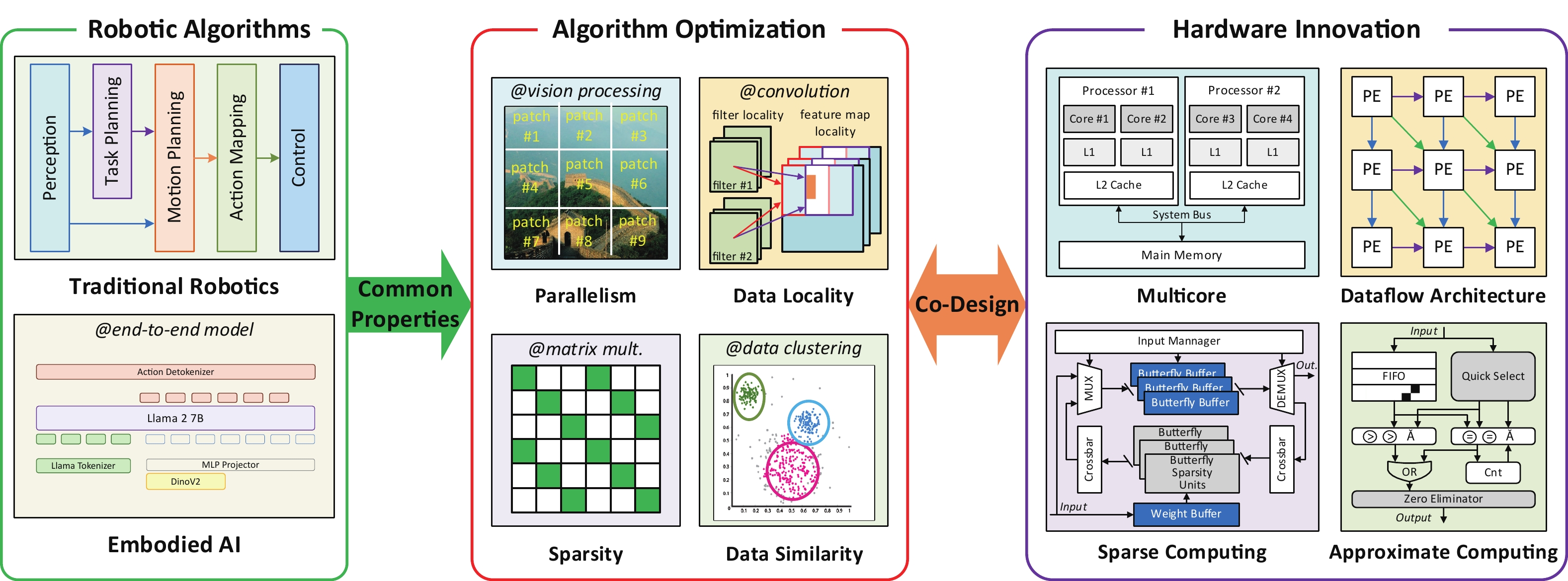
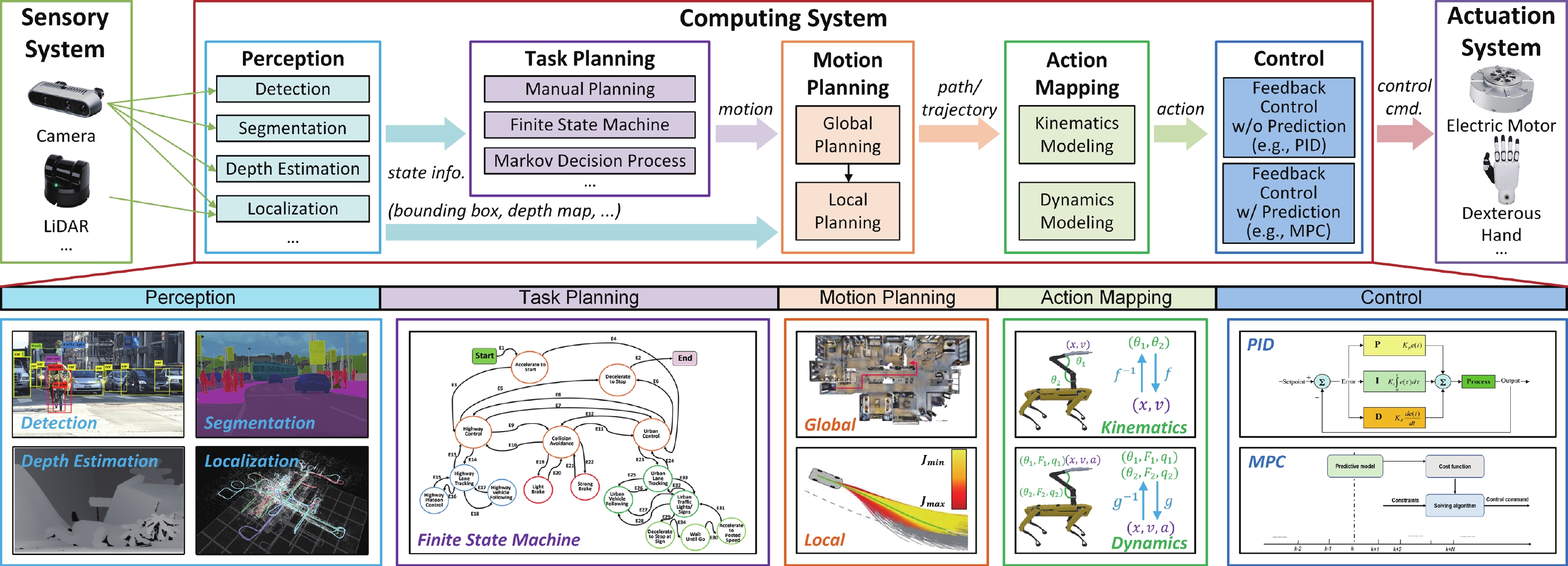
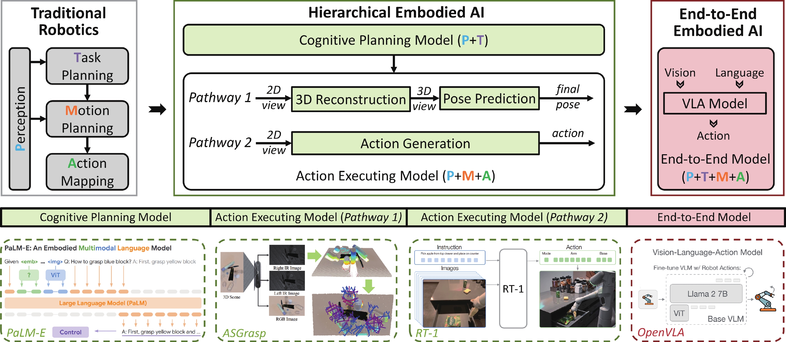
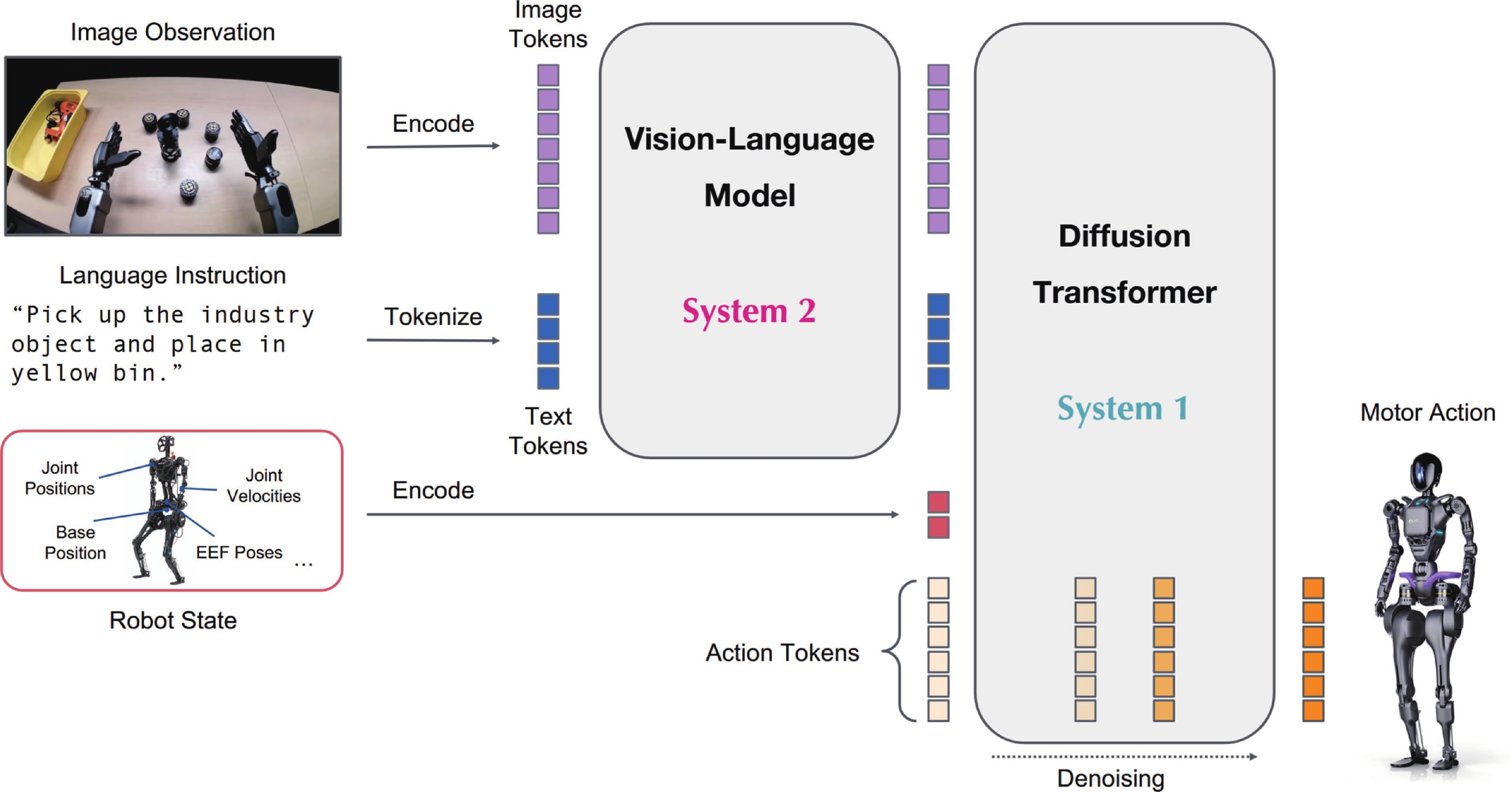
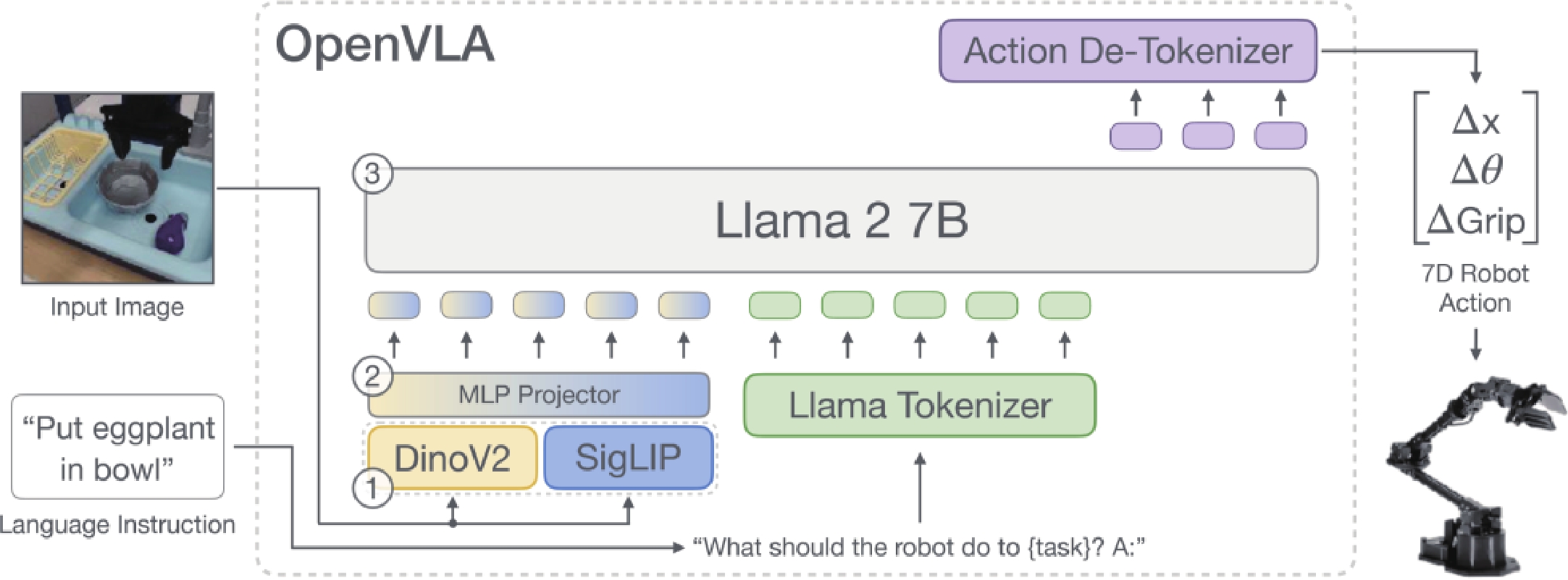
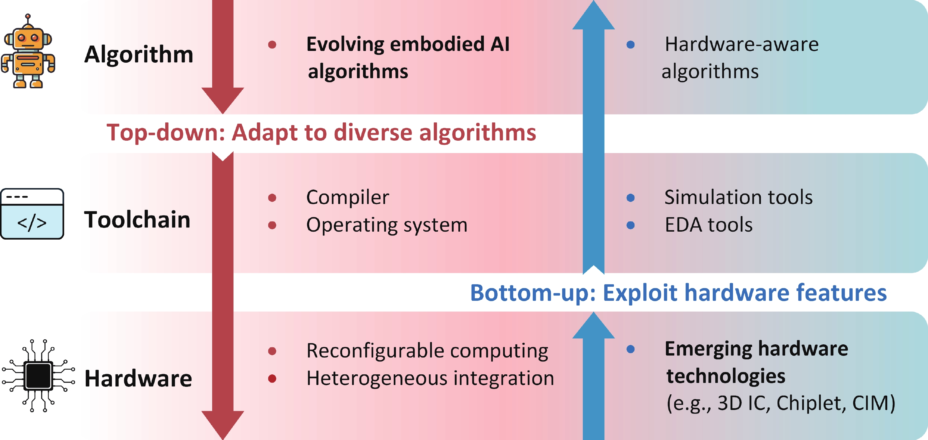
Robotic computing systems play an important role in enabling intelligent robotic tasks through intelligent algorithms and supporting hardware. In recent years, the evolution of robotic algorithms indicates a roadmap from traditional robotics to hierarchical and end-to-end models. This algorithmic advancement poses a critical challenge in achieving balanced system-wide performance. Therefore, algorithm-hardware co-design has emerged as the primary methodology, which analyzes algorithm behaviors on hardware to identify common computational properties. These properties can motivate algorithm optimization to reduce computational complexity and hardware innovation from architecture to circuit for high performance and high energy efficiency. We then reviewed recent works on robotic and embodied AI algorithms and computing hardware to demonstrate this algorithm-hardware co-design methodology. In the end, we discuss future research opportunities by answering two questions: (1) how to adapt the computing platforms to the rapid evolution of embodied AI algorithms, and (2) how to transform the potential of emerging hardware innovations into end-to-end inference improvements.
J. Semicond.
2025, 46(10): 102201 doi: 10.1088/1674-4926/25010030
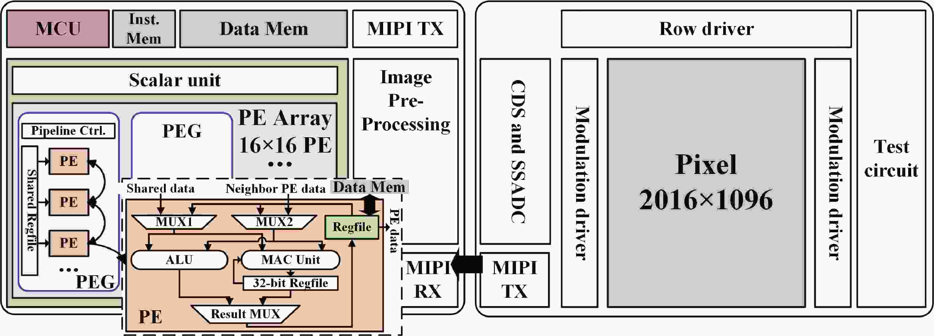
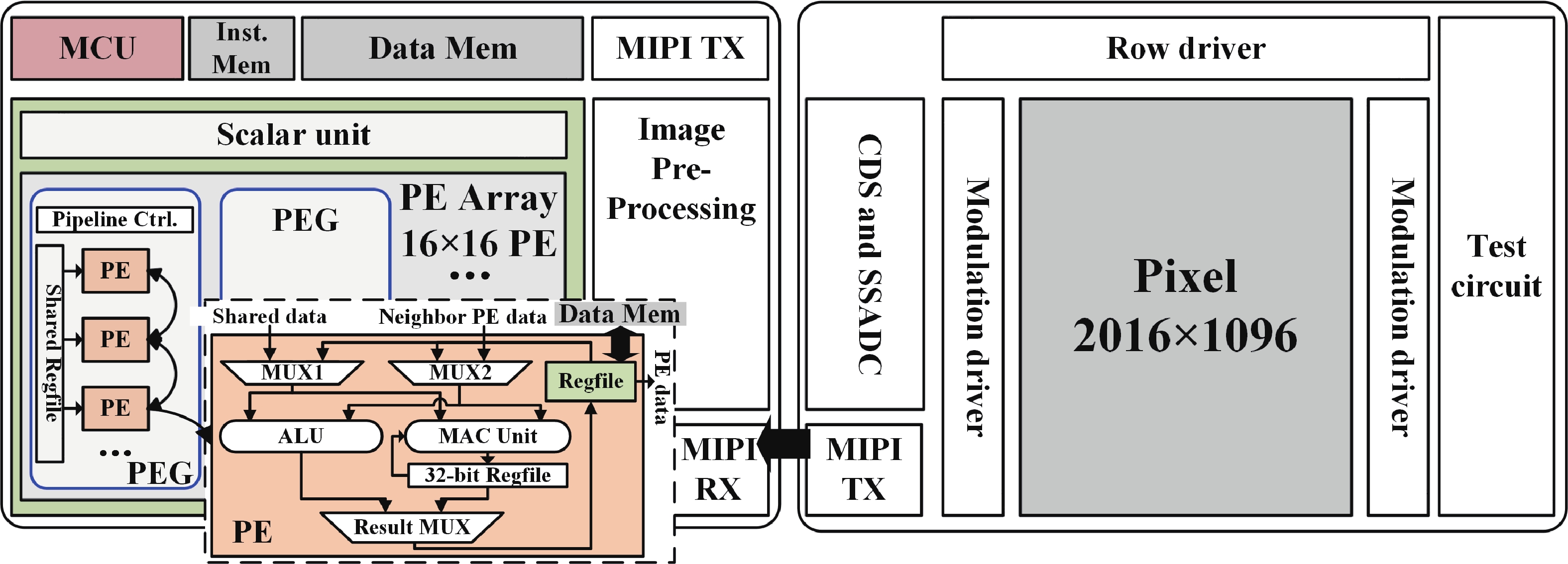
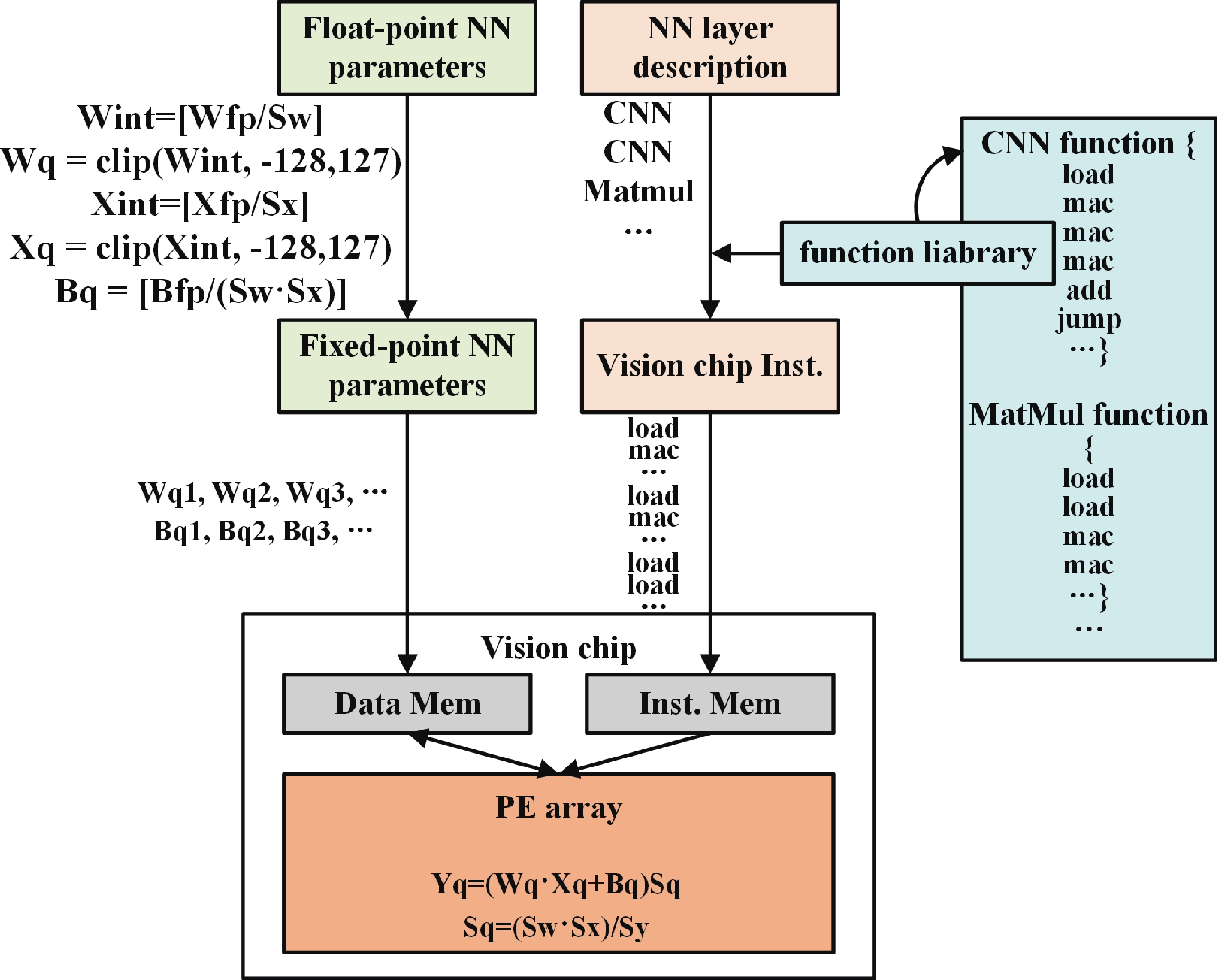
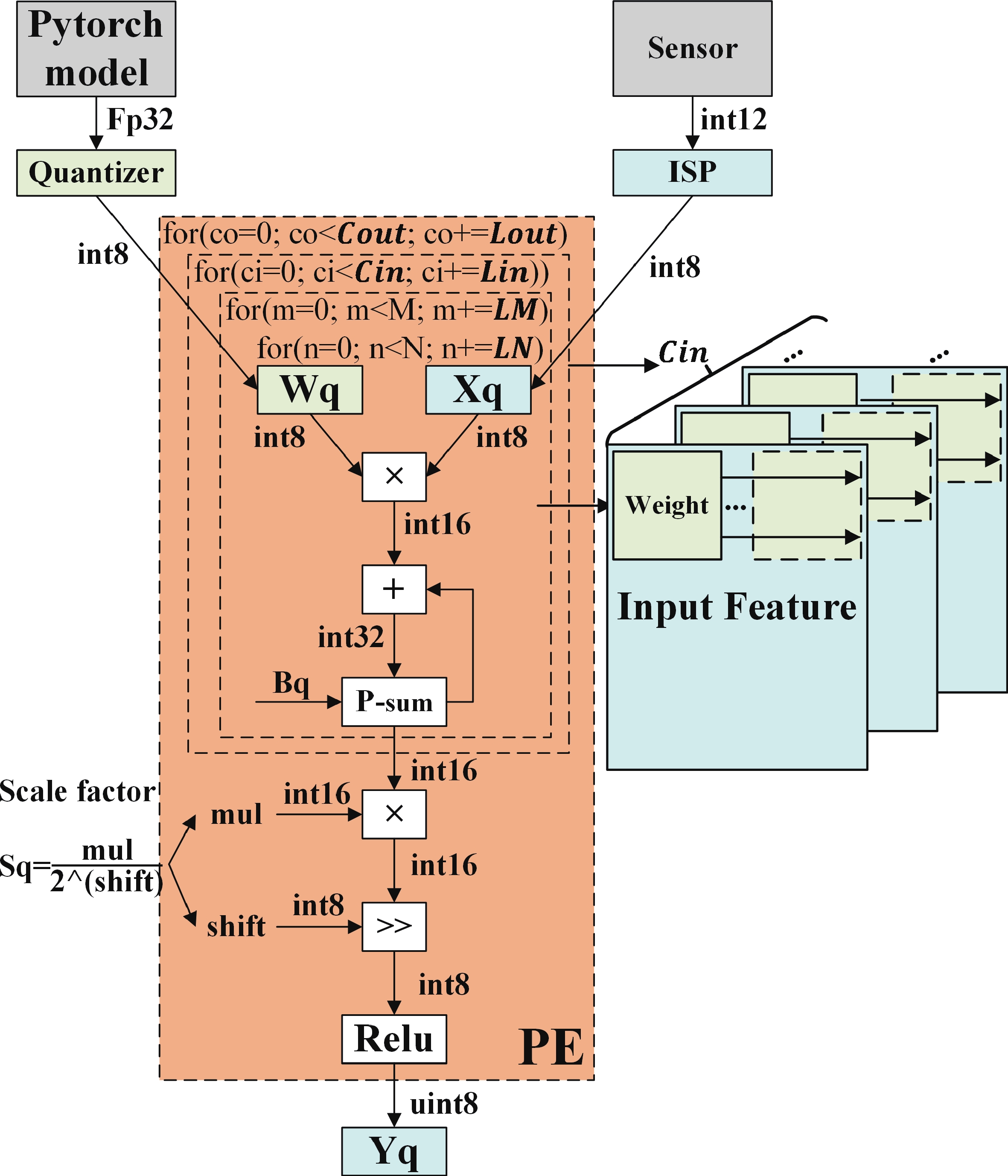
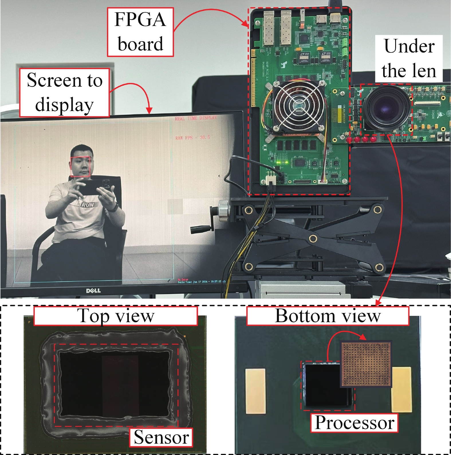
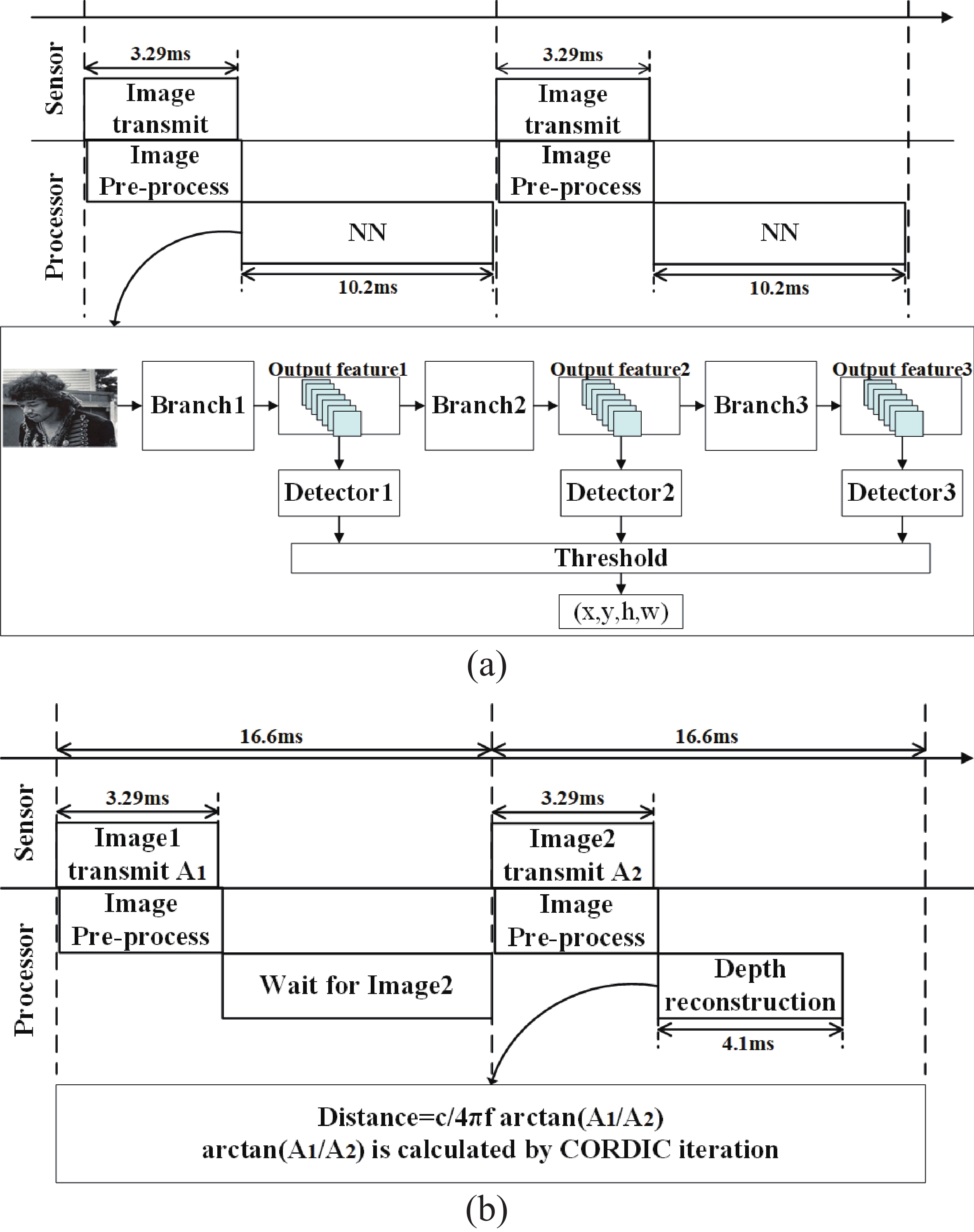
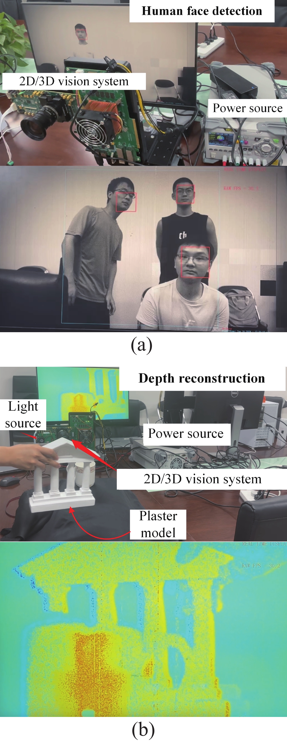
This paper describes a 2D/3D vision chip with integrated sensing and processing capabilities. The 2D/3D vision chip architecture includes a 2D/3D image sensor and a programmable visual processor. In this architecture, we design a novel on-chip processing flow with die-to-die image transmission and low-latency fixed-point image processing. The vision chip achieves real-time end-to-end processing of convolutional neural networks (CNNs) and conventional image processing algorithms. Furthermore, an end-to-end 2D/3D vision system is built to exhibit the capacity of the vision chip. The vision system achieves real-timing applications under 2D and 3D scenes, such as human face detection (processing delay 10.2 ms) and depth map reconstruction (processing delay 4.1 ms). The frame rate of image acquisition, image process, and result display is larger than 30 fps.
J. Semicond.
2025, 46(10): 102202 doi: 10.1088/1674-4926/25020011
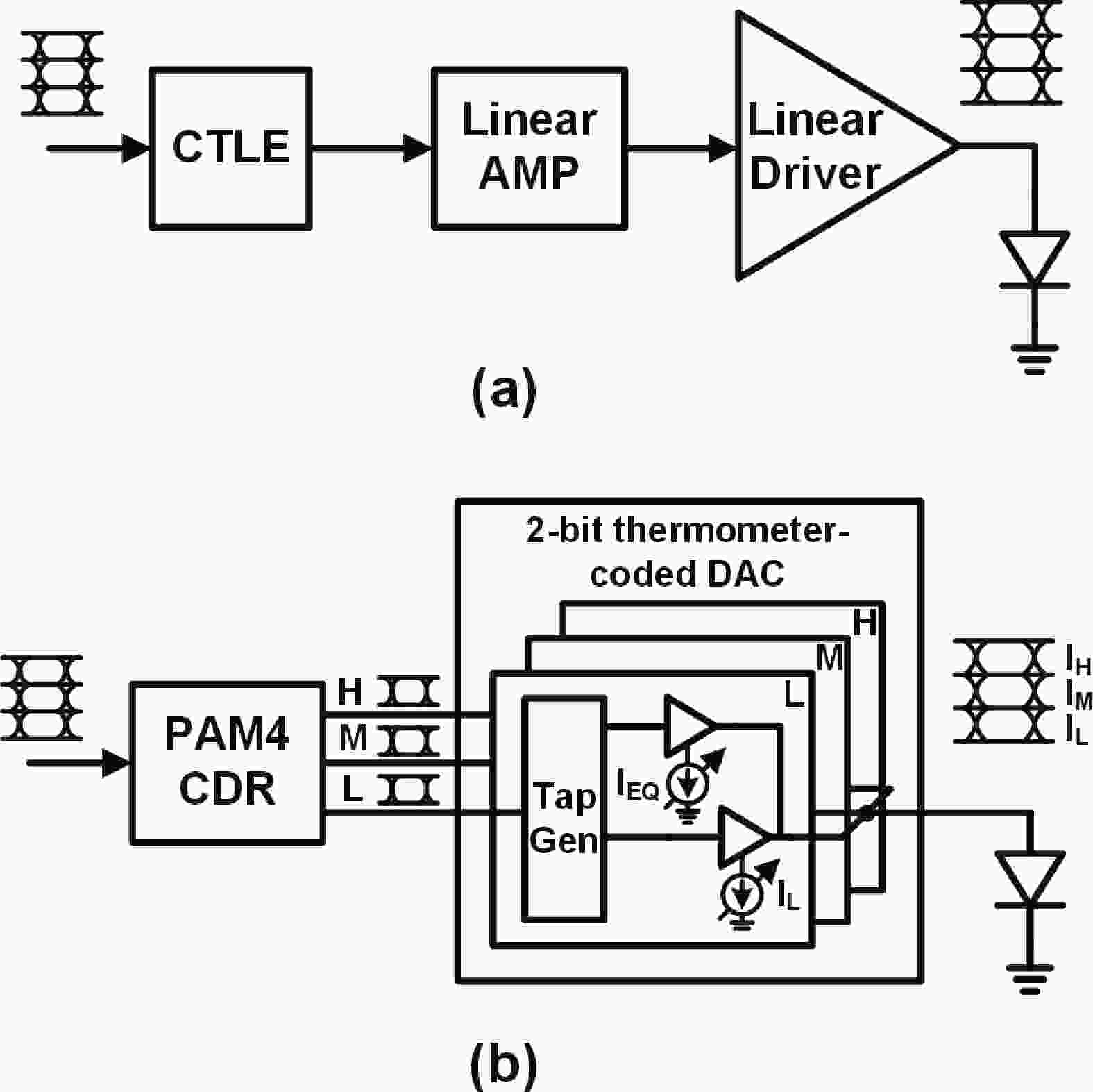
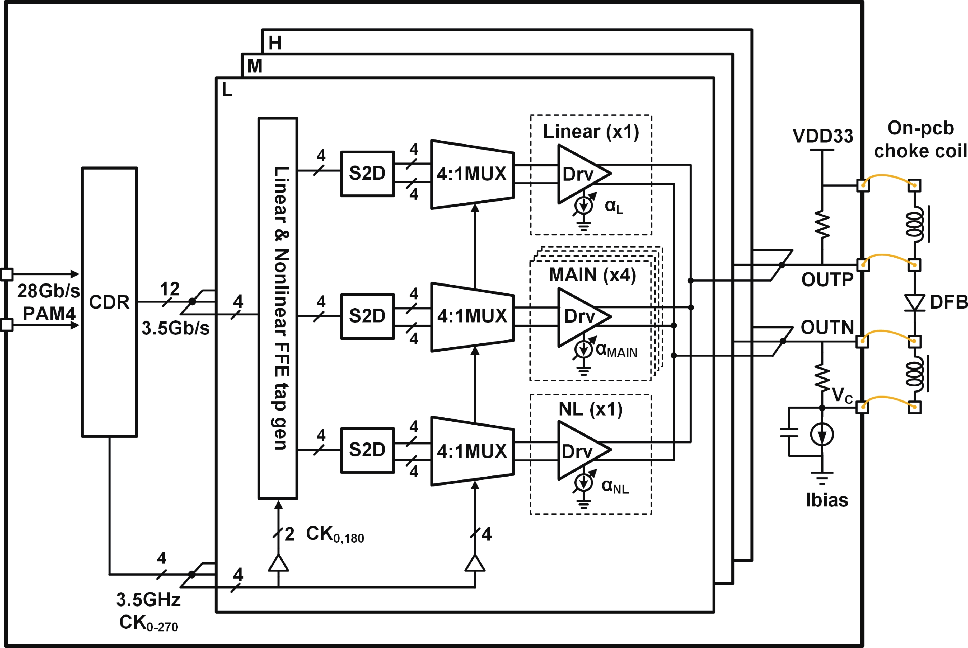
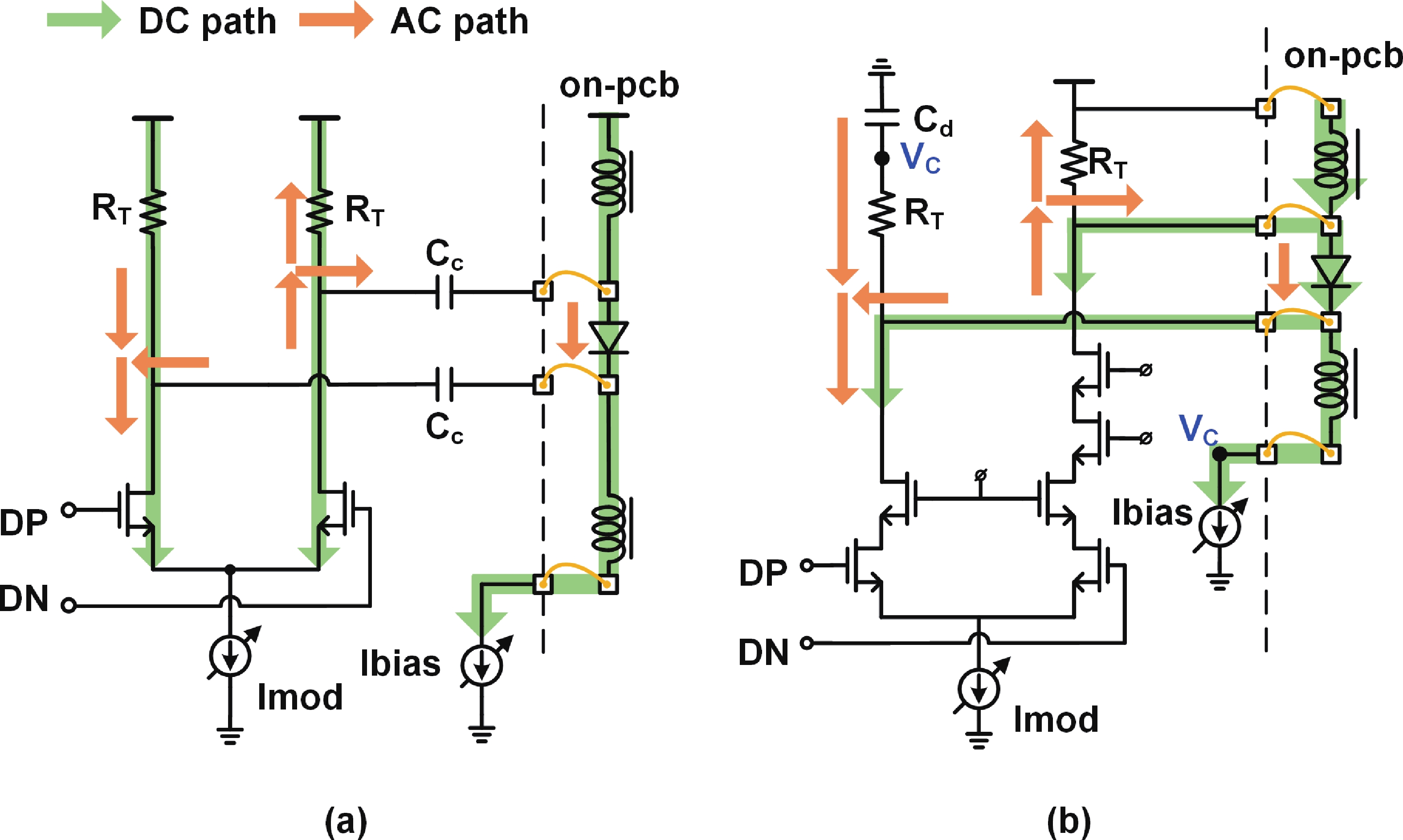
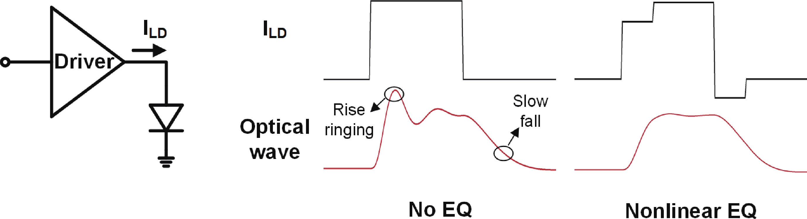
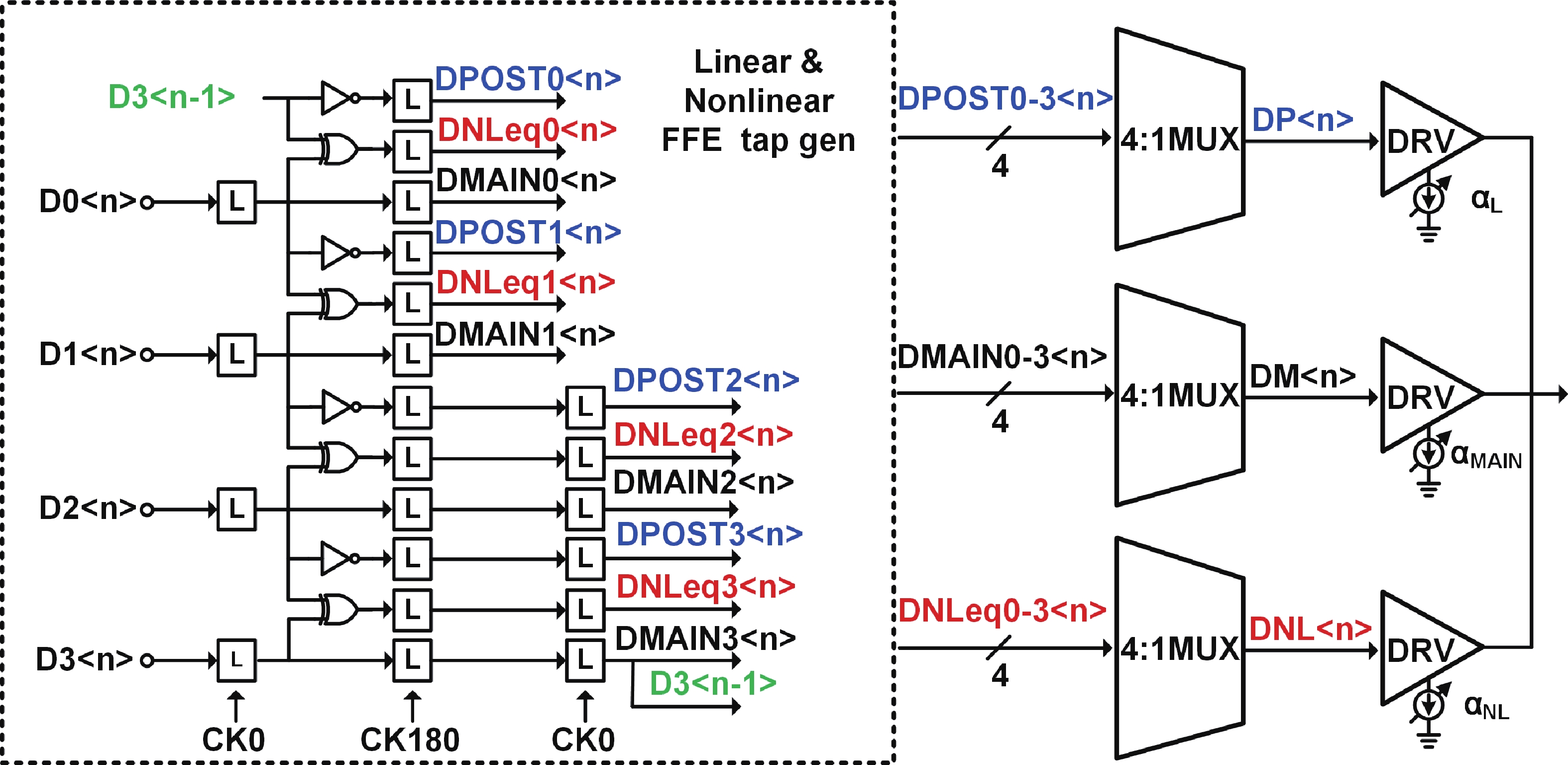
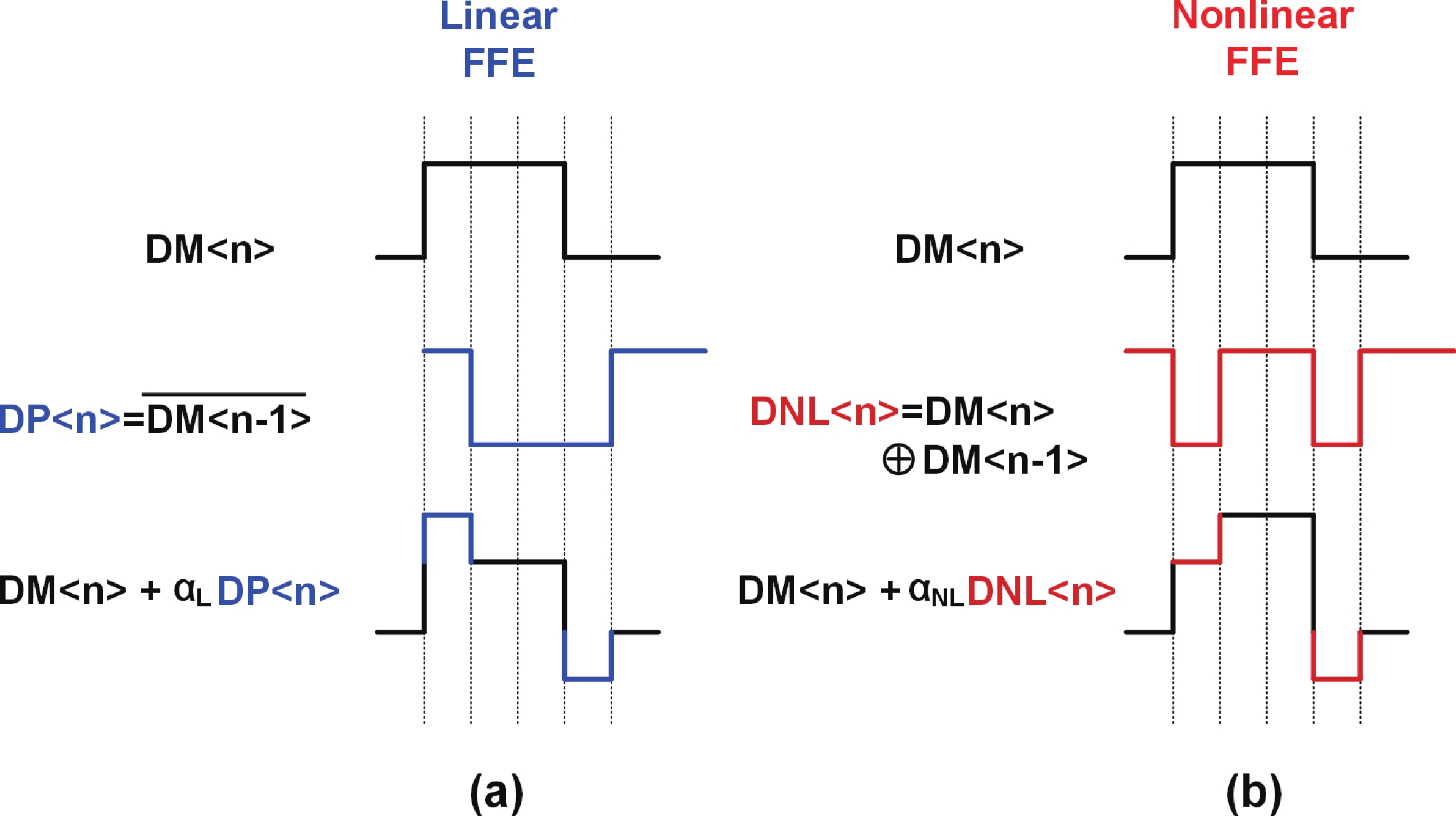
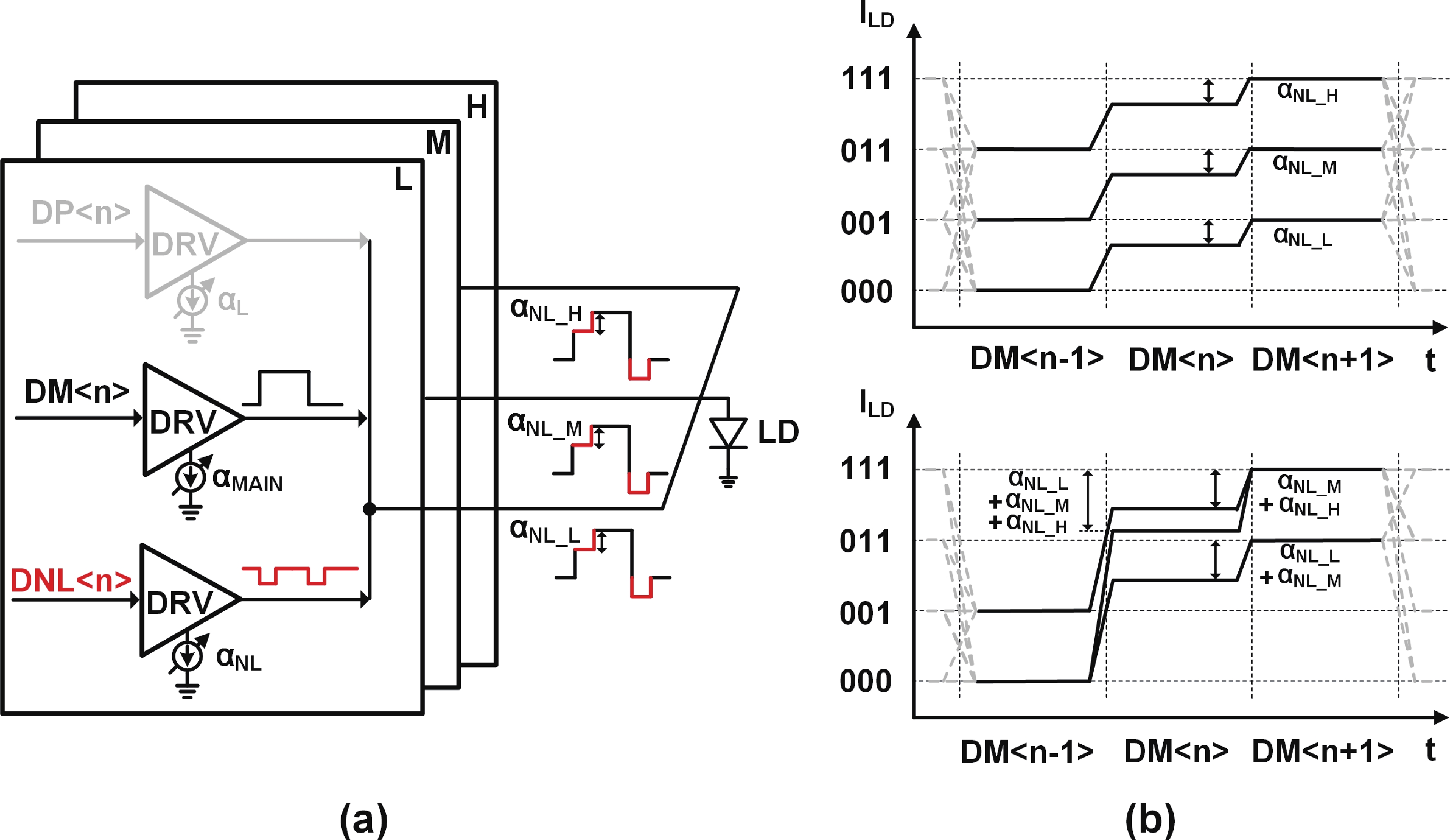
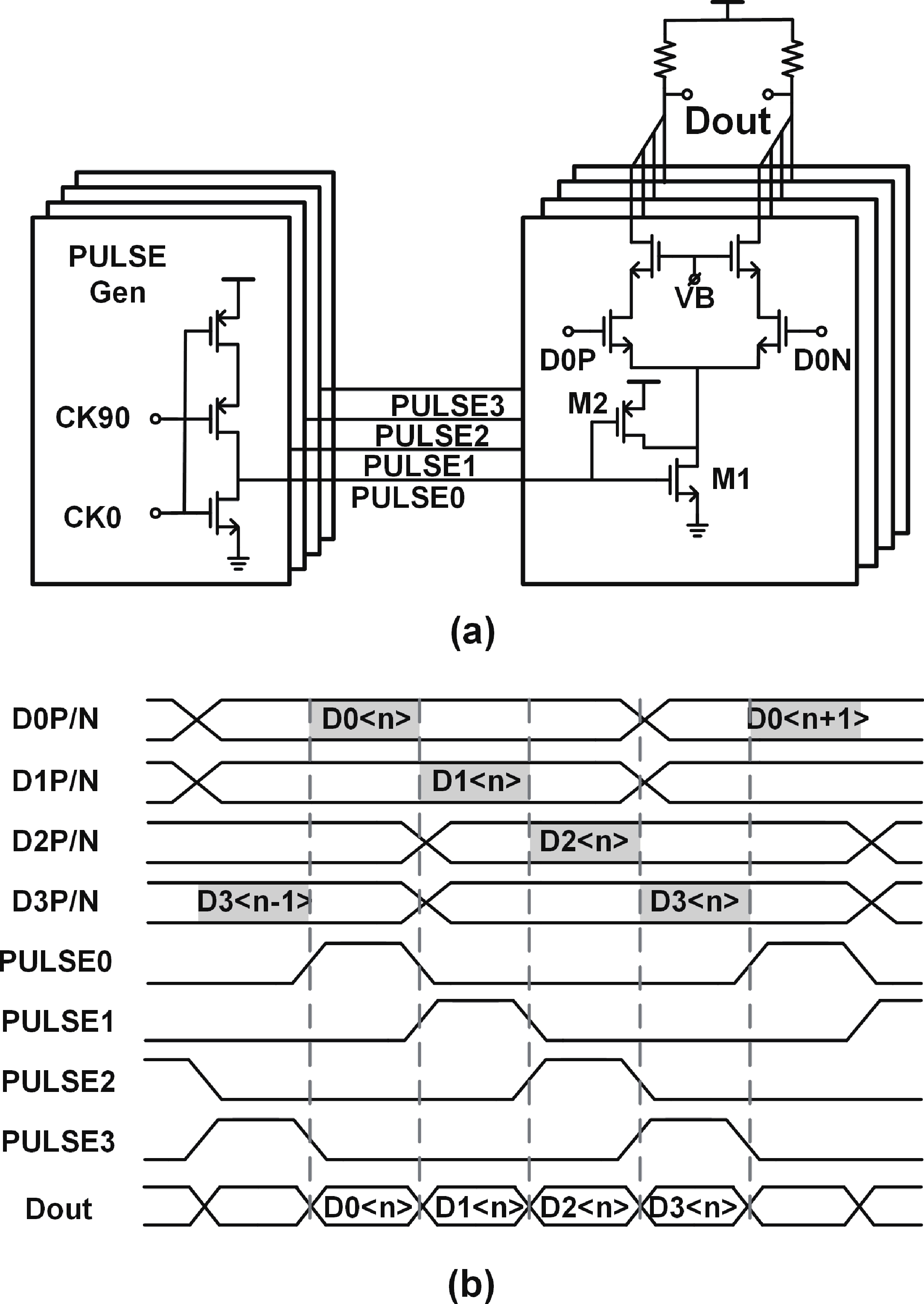
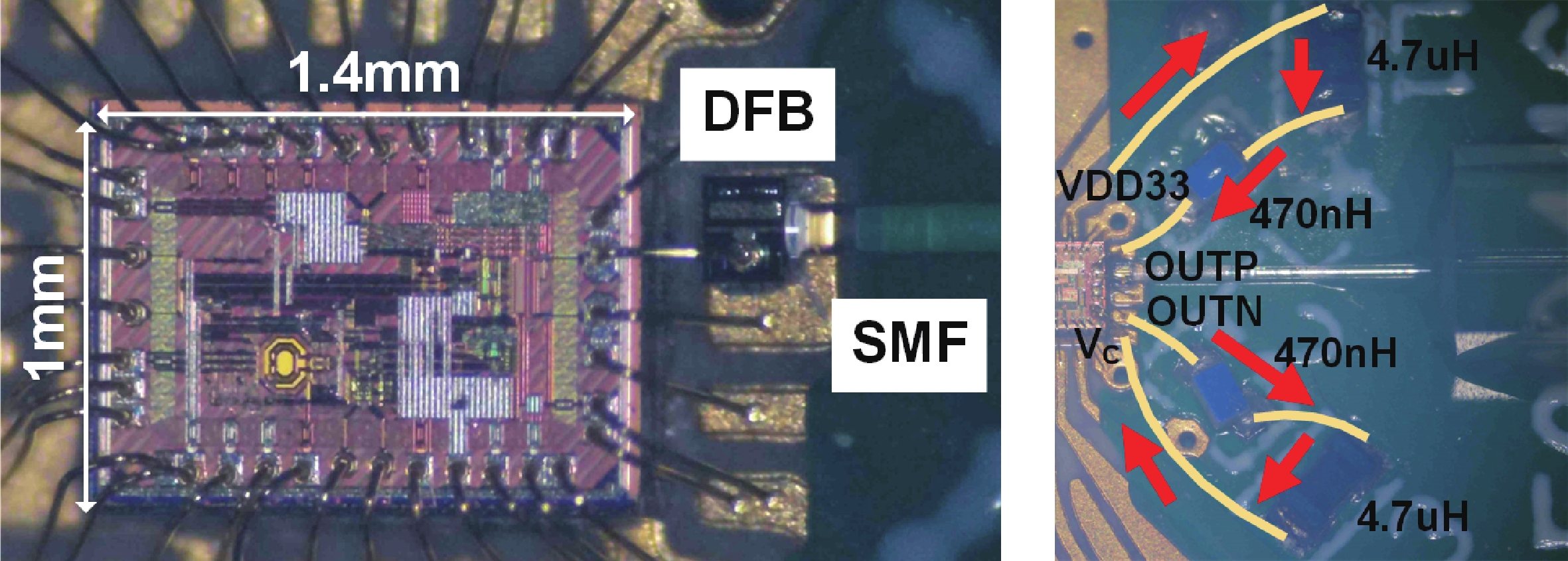
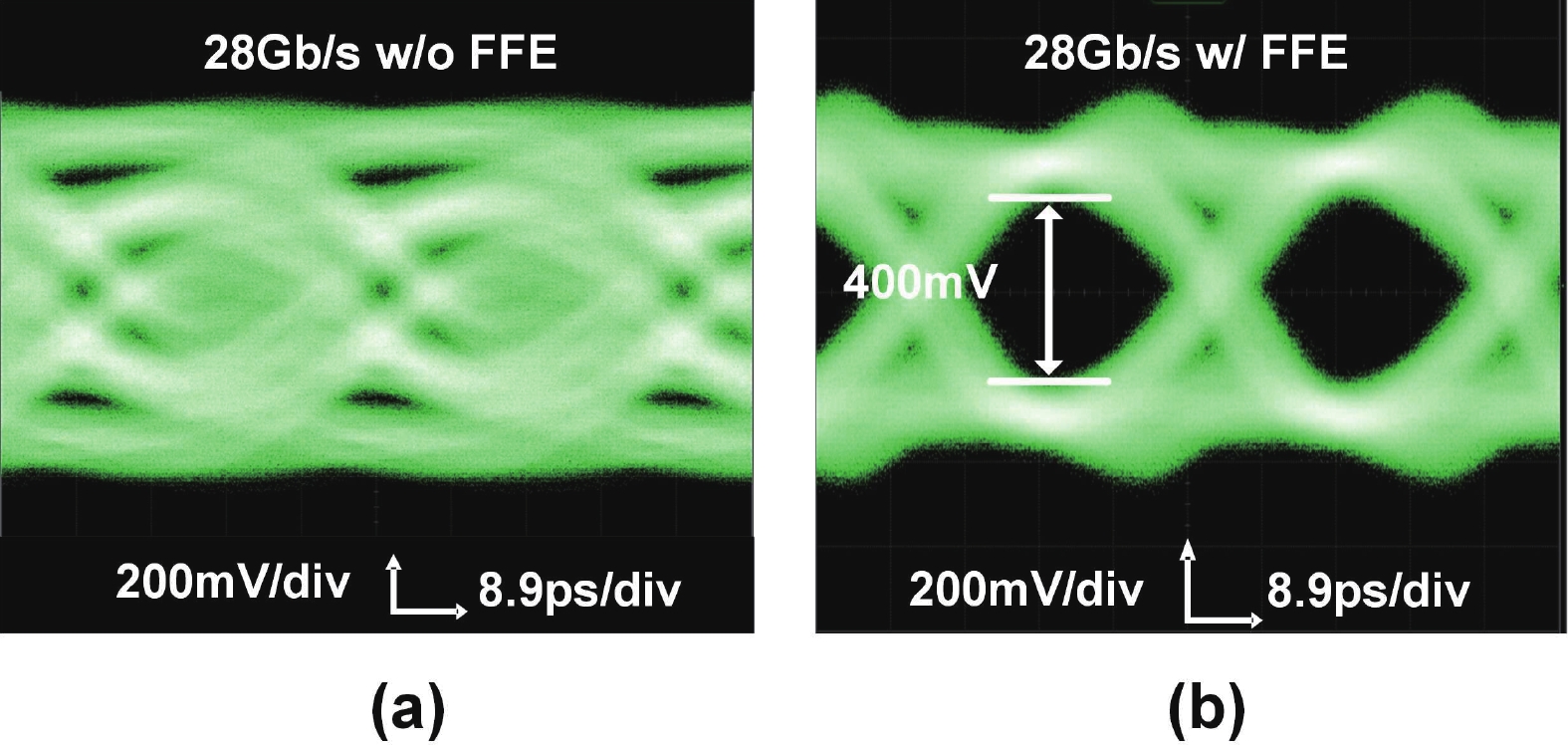
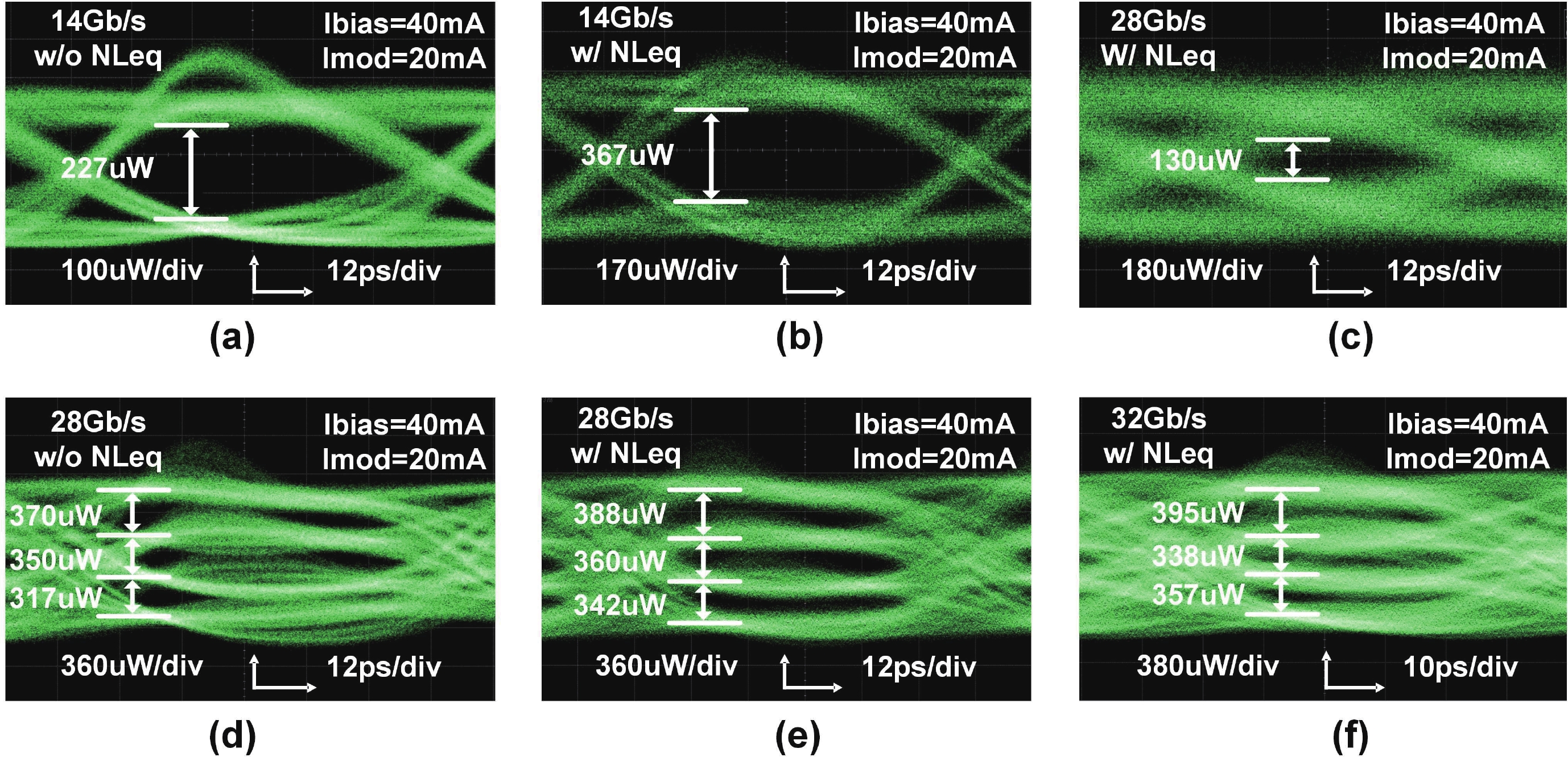
This paper presents a 4-level pulse amplitude modulation (PAM-4) distributed feedback (DFB) laser driver. The driver adopts a digital slicing architecture to achieve high linearity by adjusting the weights of three thermometer-coded main paths. An efficient-biased output stage structure is proposed to reduce power consumption while avoiding the degradation of output node bandwidth typically induced by parasitic capacitance in high-current bias path. A two-tap linear and nonlinear feed-forward equalizer (FFE) is implemented in the digital domain to extend bandwidth limitations and compensate for the dynamic nonlinearity of the DFB laser. The nonlinear FFE is realized at the cost of lower power consumption and smaller area by utilizing the simultaneity of low-speed parallel data. The chip is fabricated in 28 nm CMOS process. Measurement results indicate that, with a laser bias current of 40 mA, a modulation current of 20 mApp, and an operating rate of 32 Gb/s PAM-4, the overall power consumption of the chip is 372 mW, corresponding to an energy efficiency of 11.6 pJ/b.
J. Semicond.
2025, 46(10): 102203 doi: 10.1088/1674-4926/24120034
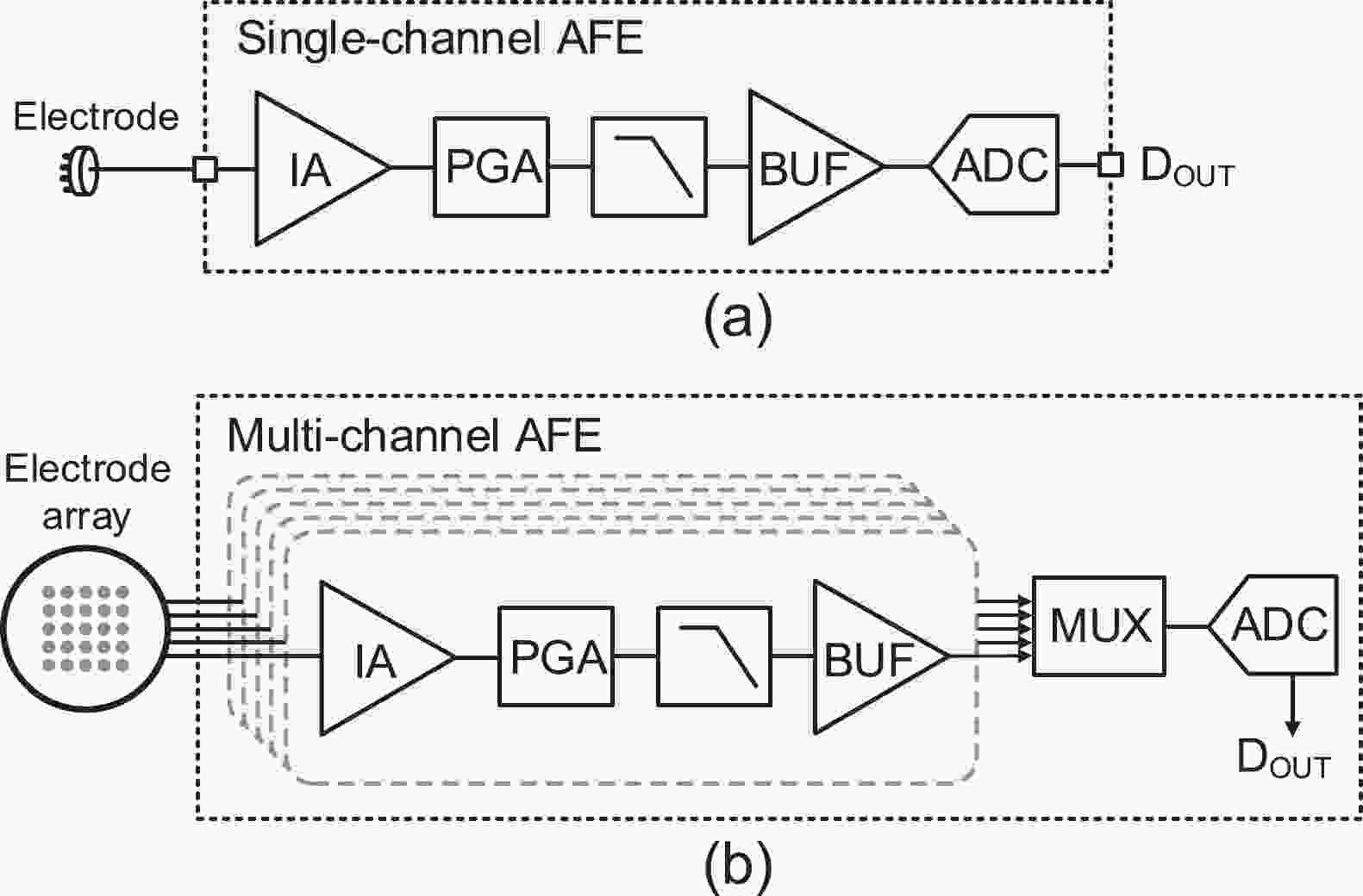
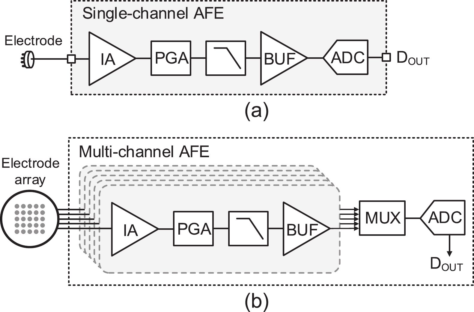
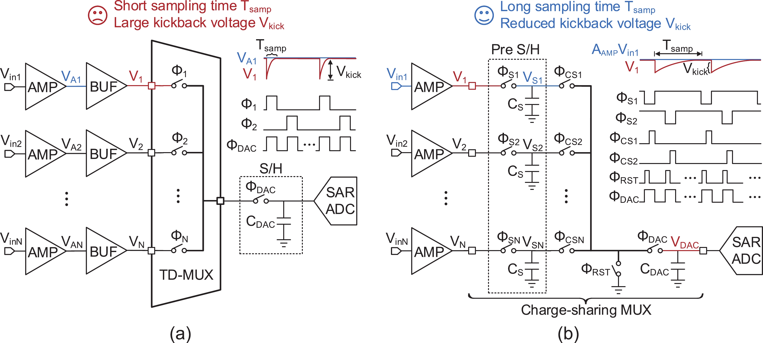
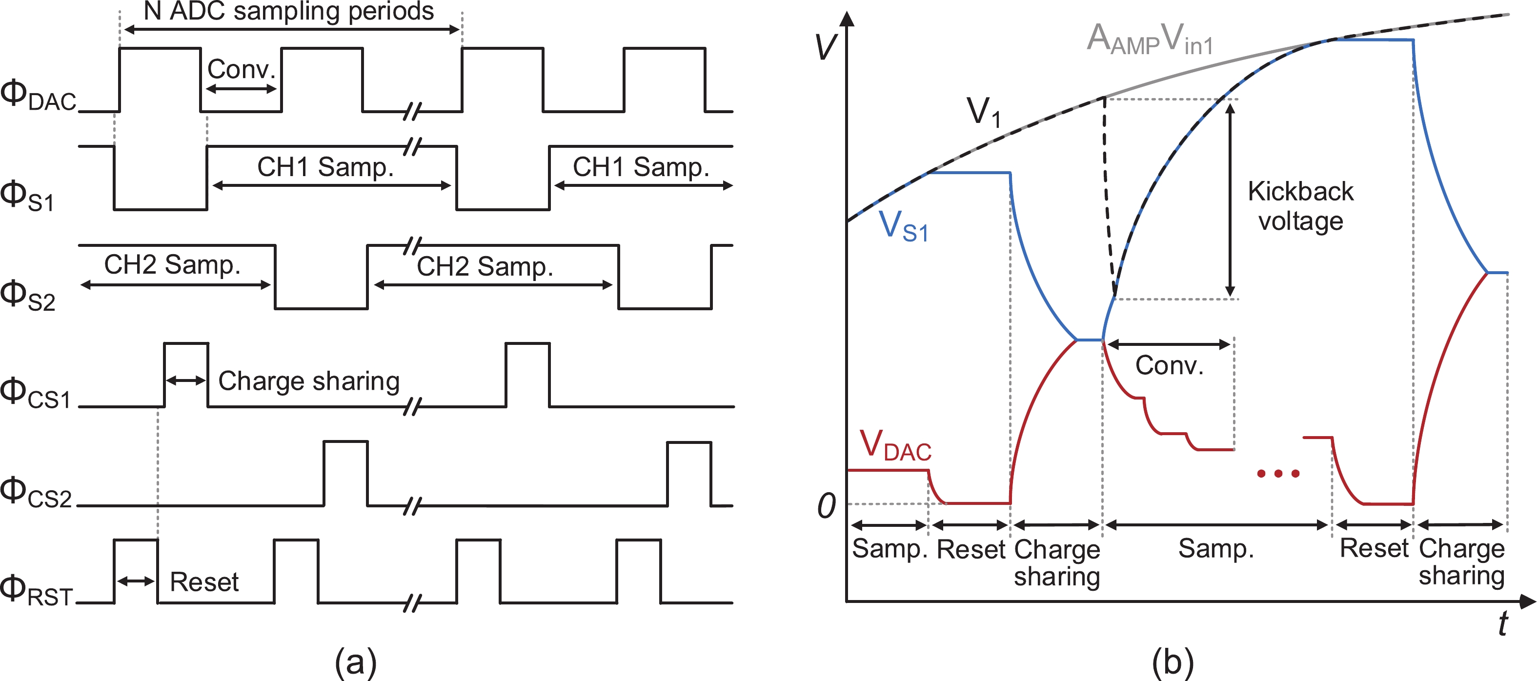
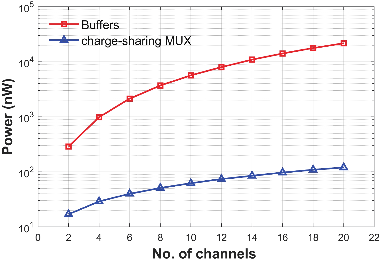
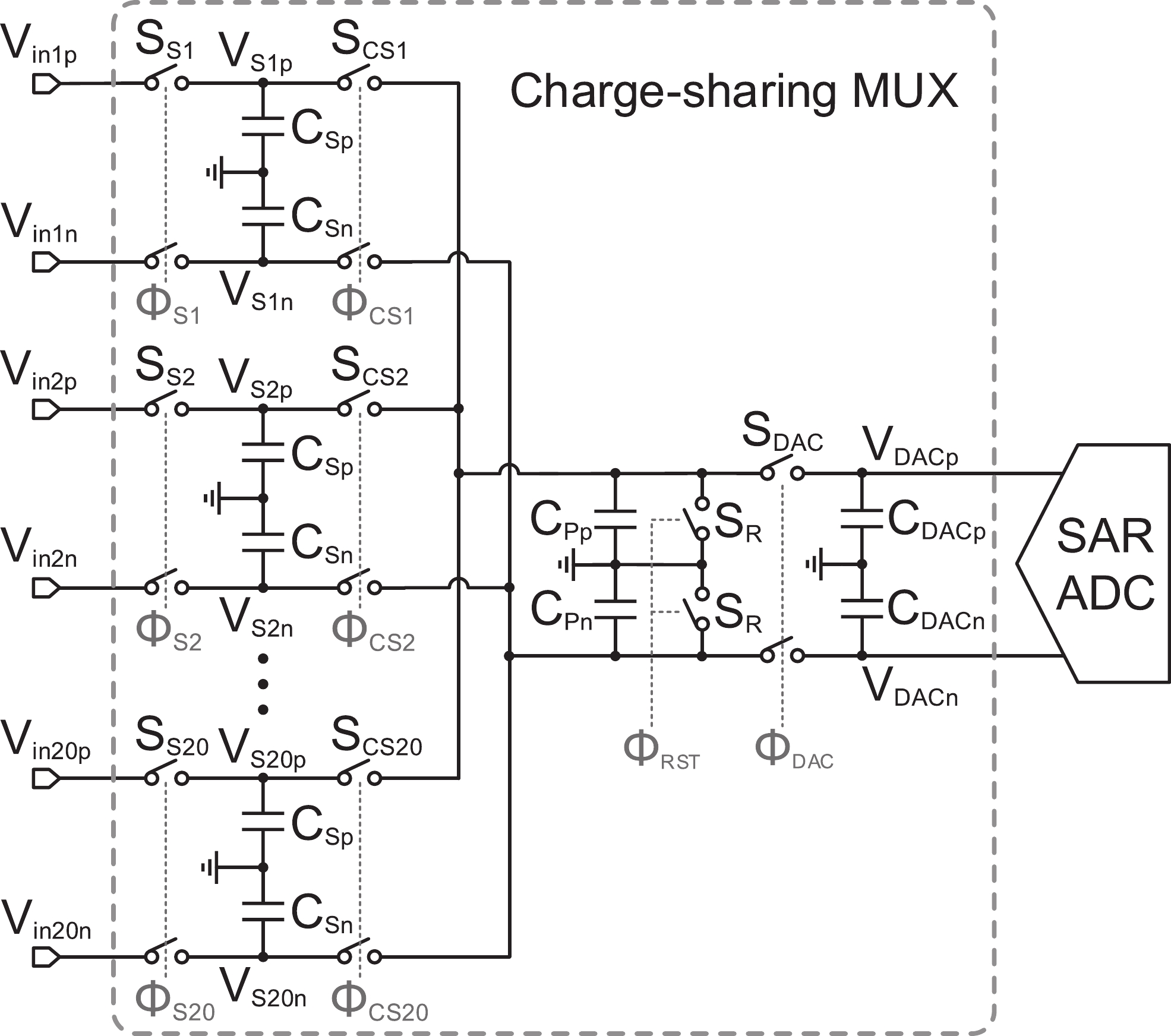
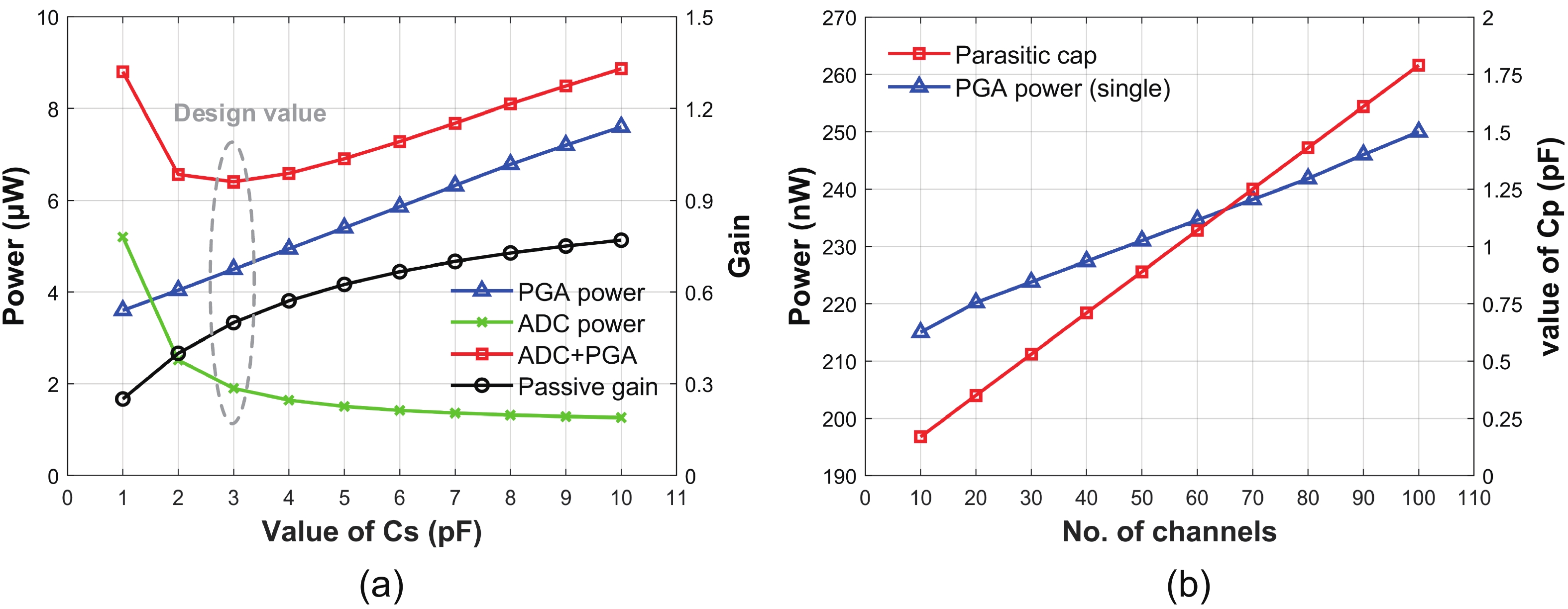
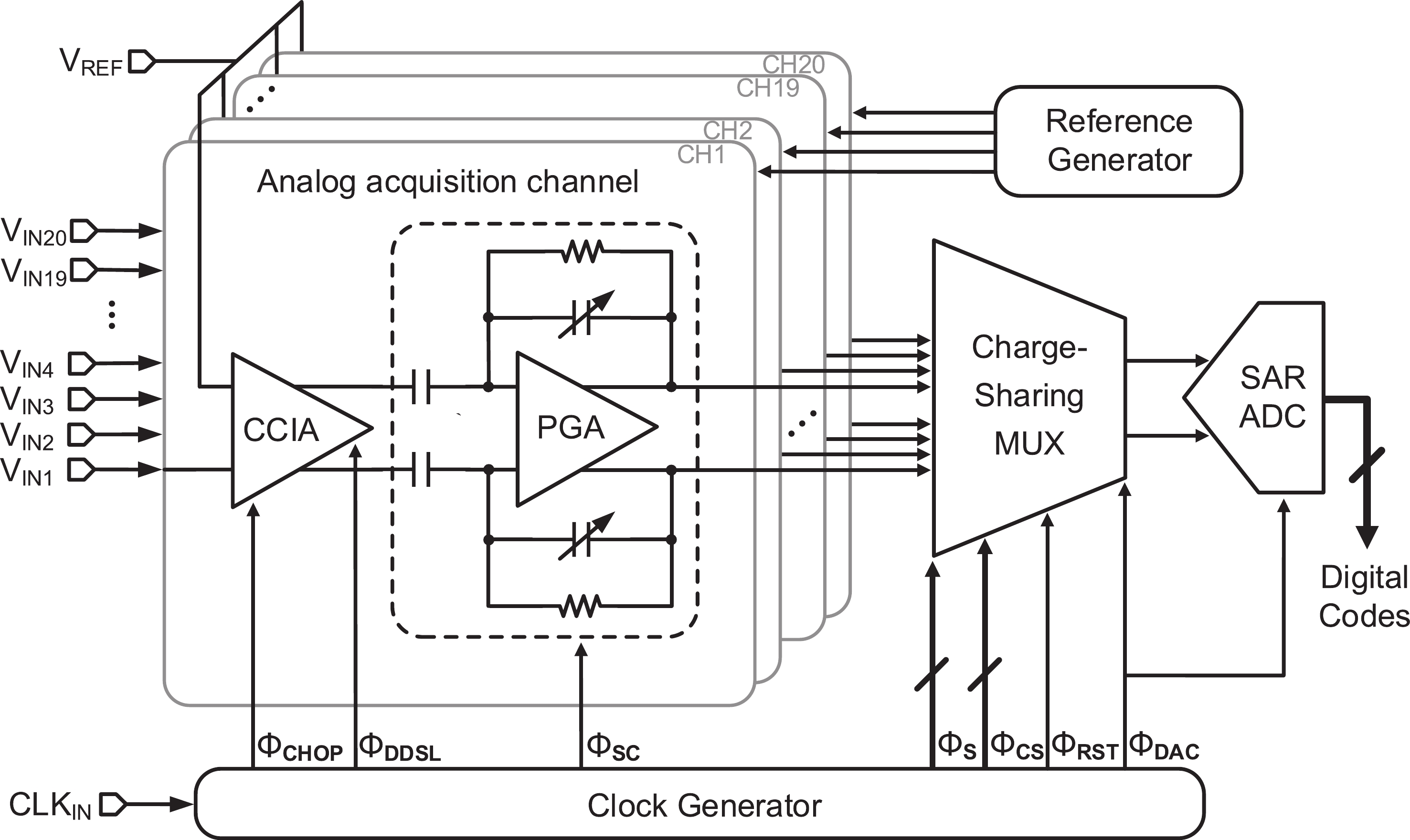
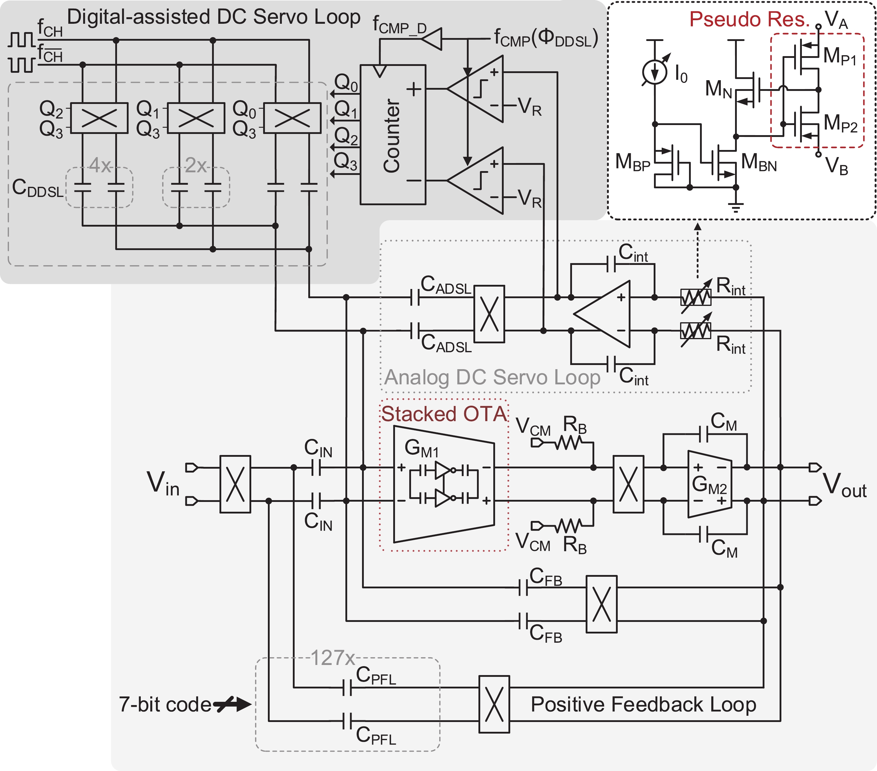
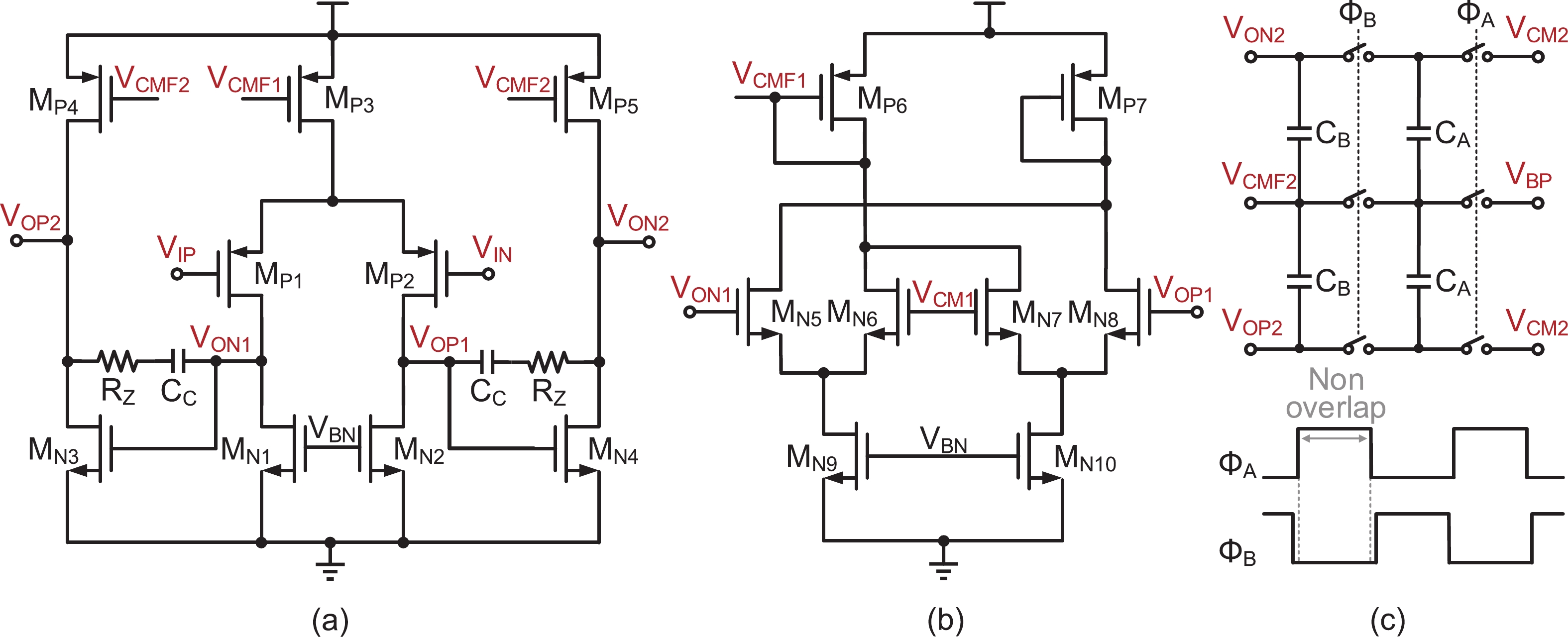
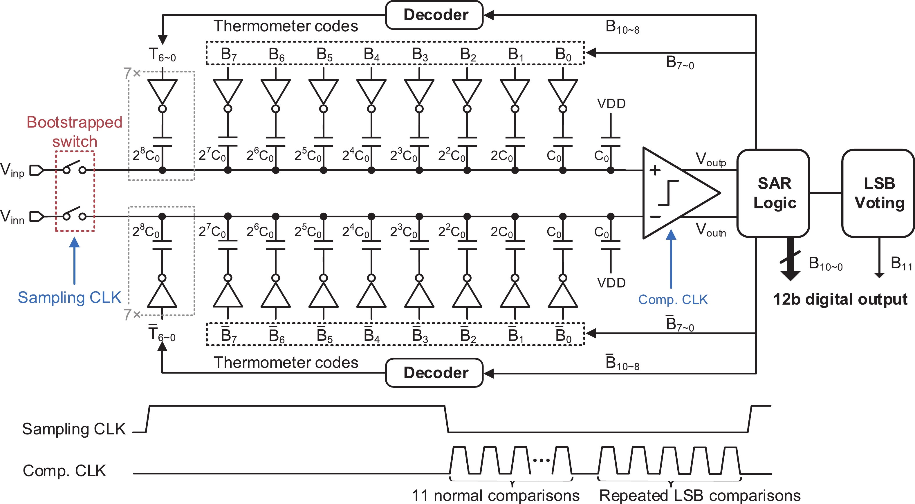
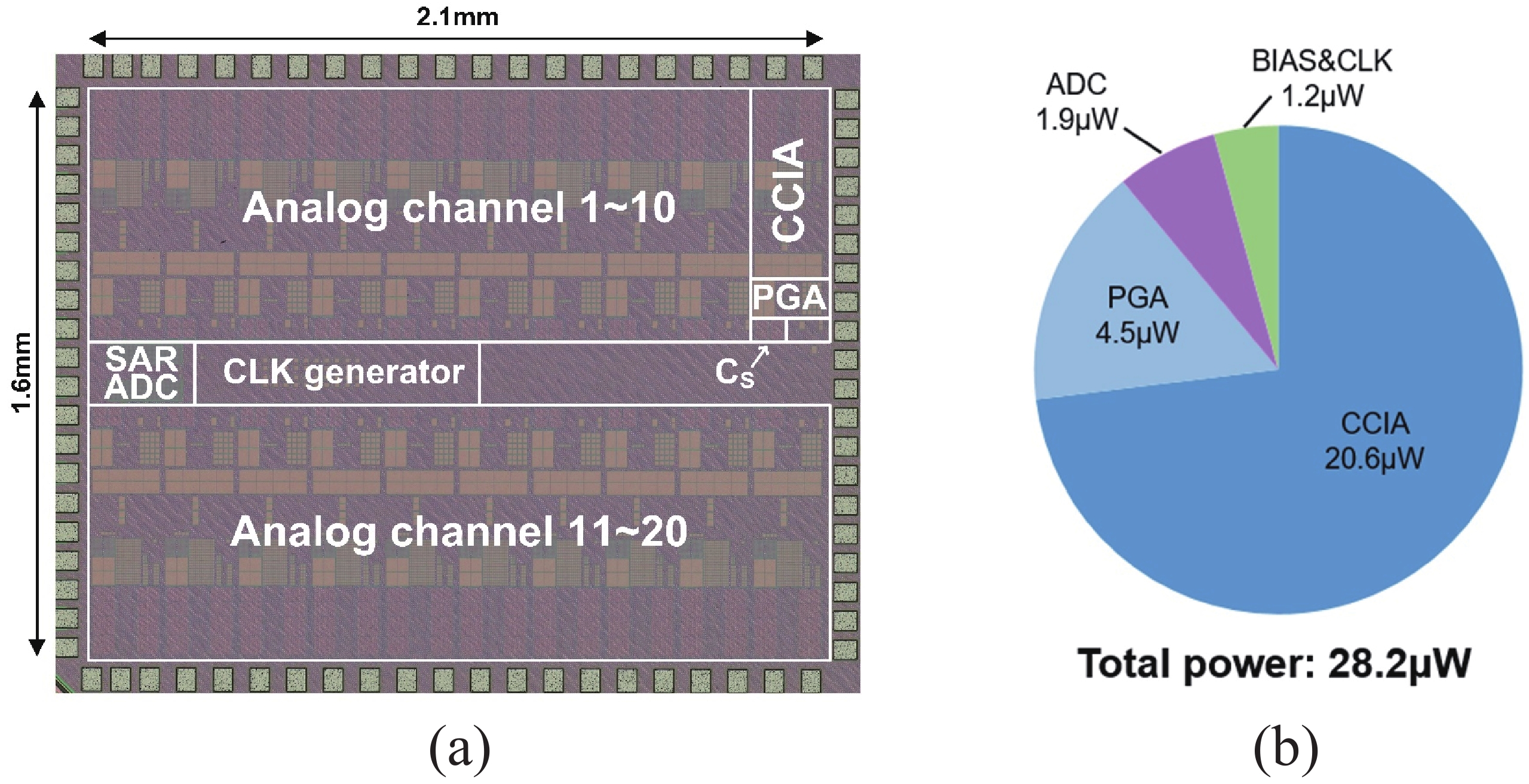
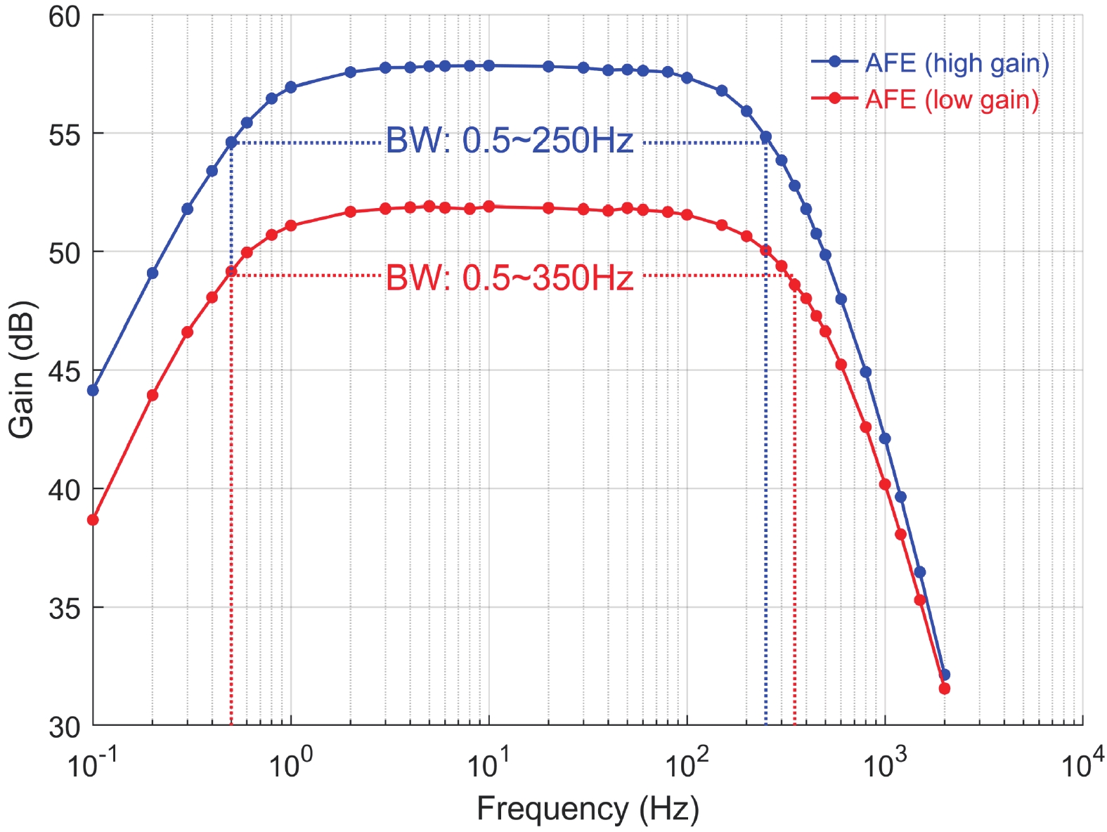
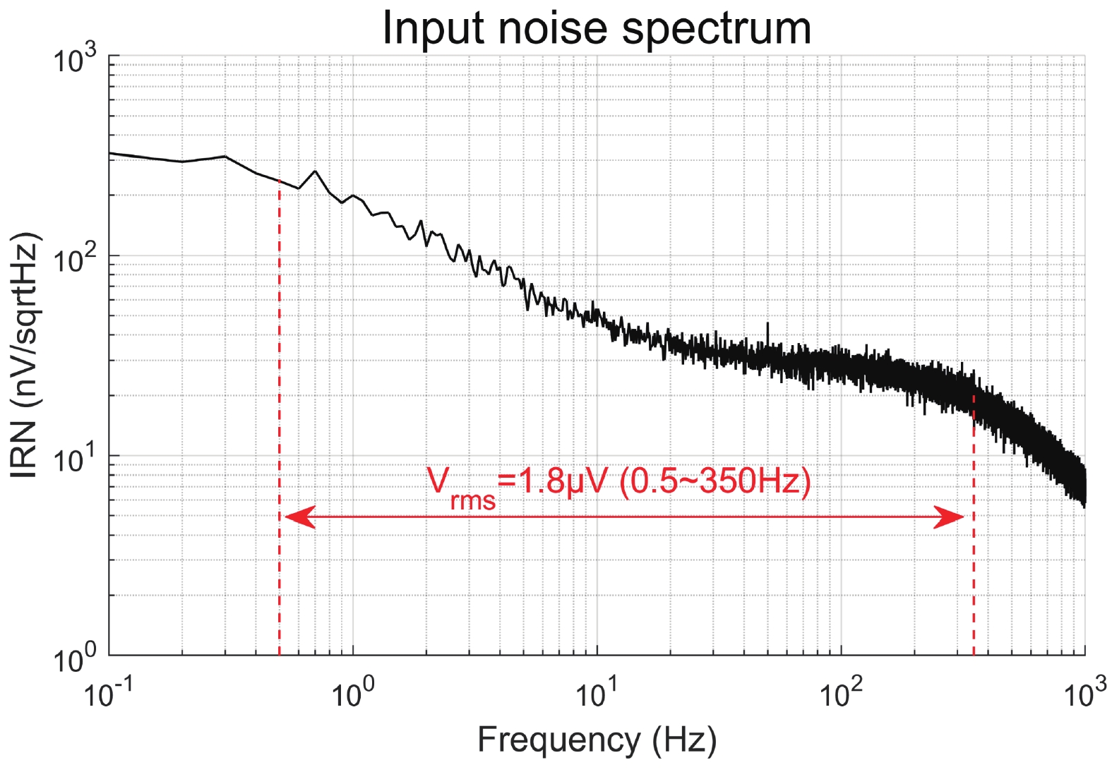
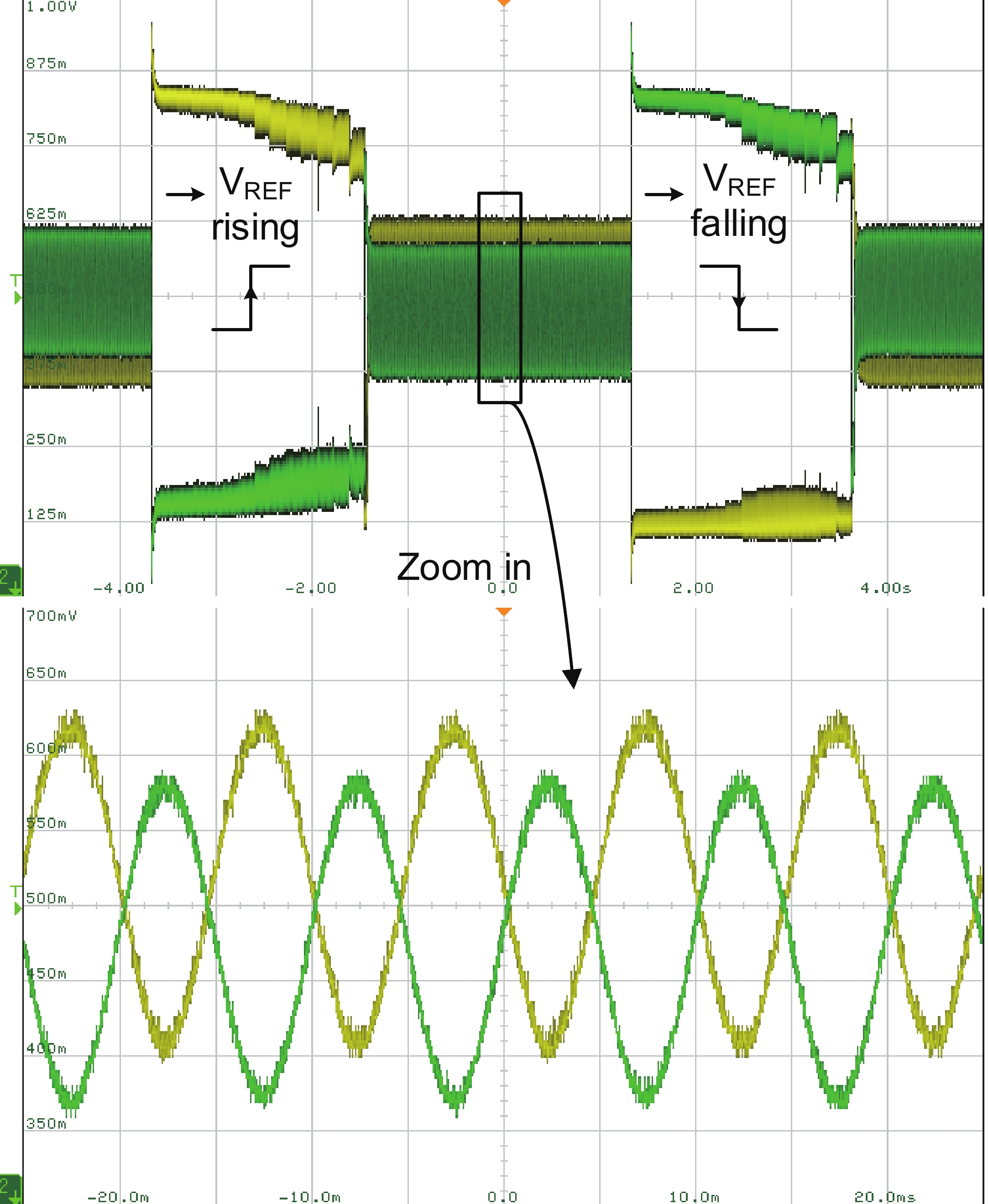
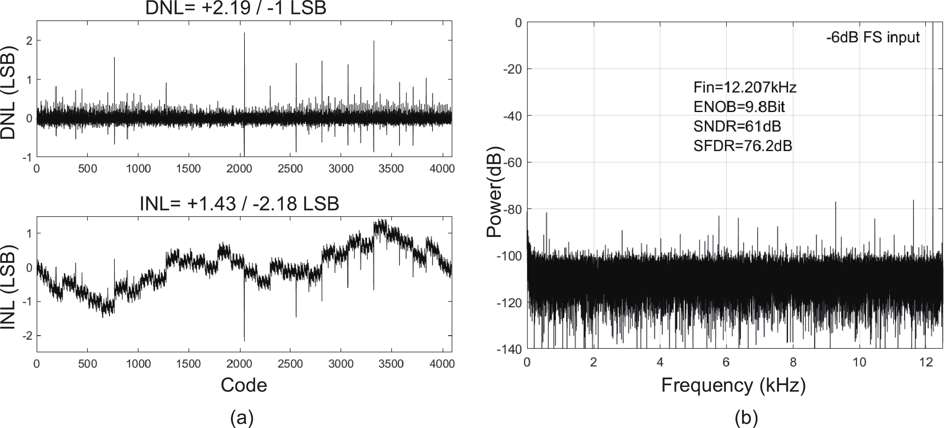
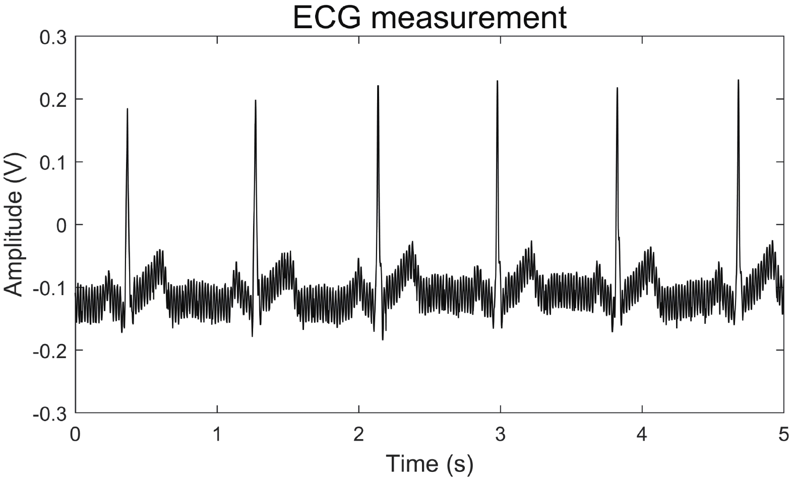
This paper presents the design of a low-power multi-channel analog front-end (AFE) for bio-potential recording. By using time division multiplexing (TDM), a successive approximation register analog-to-digital converter (SAR ADC) is shared among all 20 channels. A charge-sharing multiplexer (MUX) is proposed to transmit the output signals from the respective channels to the ADC. By separately pre sampling the output of each channel, the sampling time of each channel is greatly extended and additional active buffers are avoided. The AFE is fabricated in a 65-nm CMOS process, and the whole system consumes 28.2 μW under 1 V supply. Each analog acquisition channel consumes 1.25 μW and occupies a chip area of 0.14 mm2. Measurement results show that the AFE achieves an input referred noise of 1.8 μV∙rms in a 350 Hz bandwidth and a noise efficiency factor (NEF) of 4.1. The 12-bit SAR ADC achieves an ENOB of 9.8 bit operating at 25 kS/s. The AFE is experimented on real-world applications by measuring human ECG and a clear ECG waveform is captured.
J. Semicond.
2025, 46(10): 102401 doi: 10.1088/1674-4926/25030017
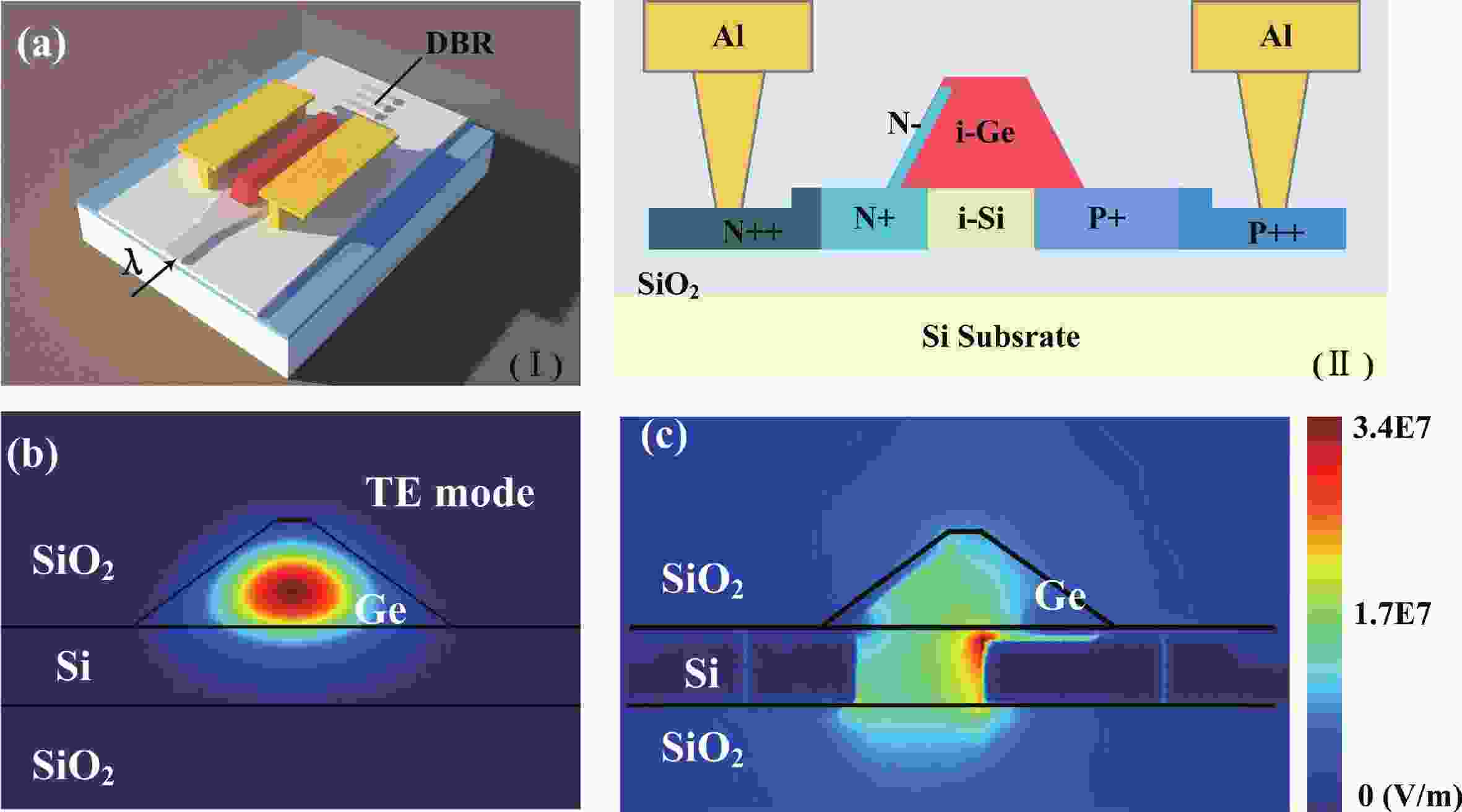
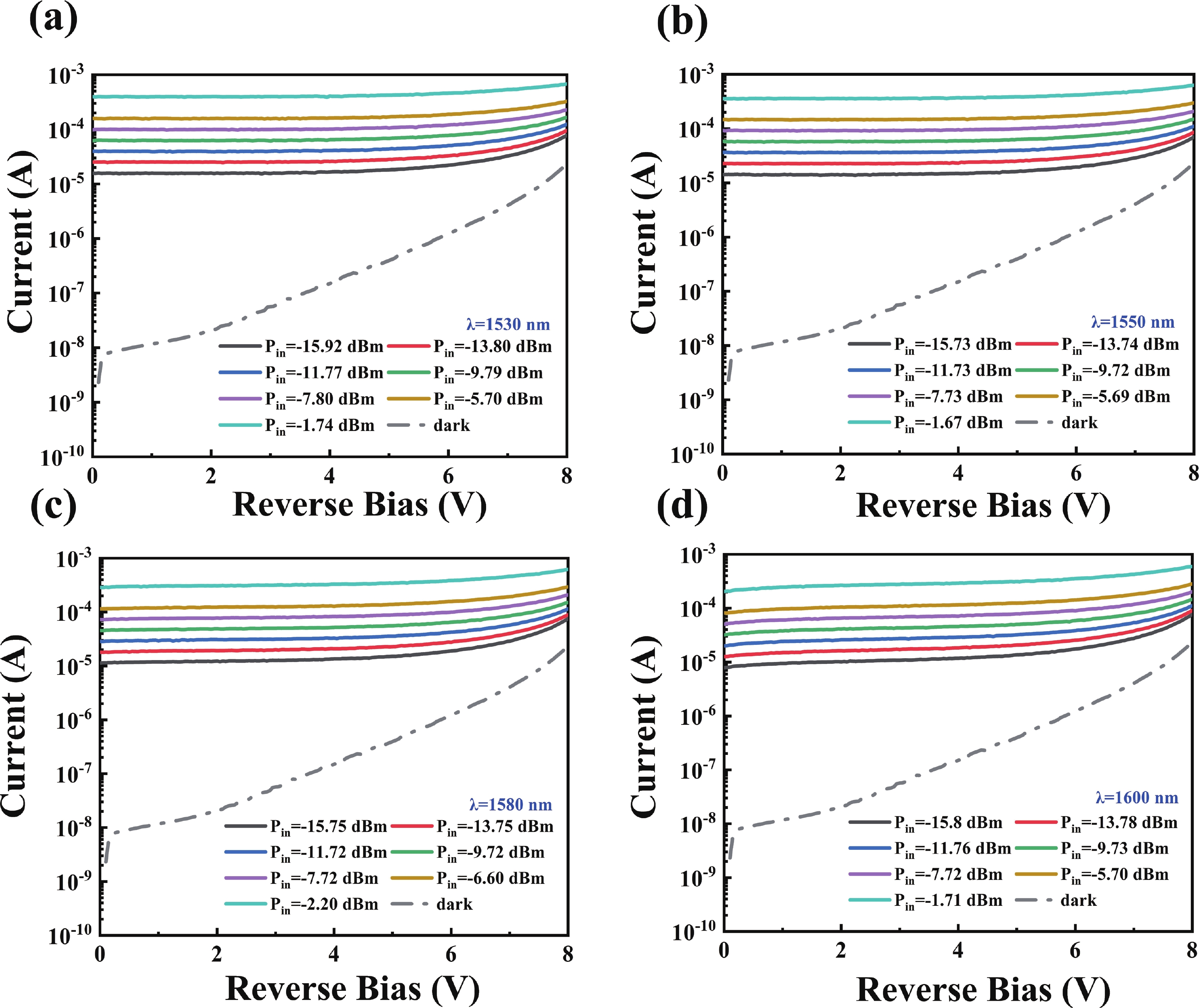
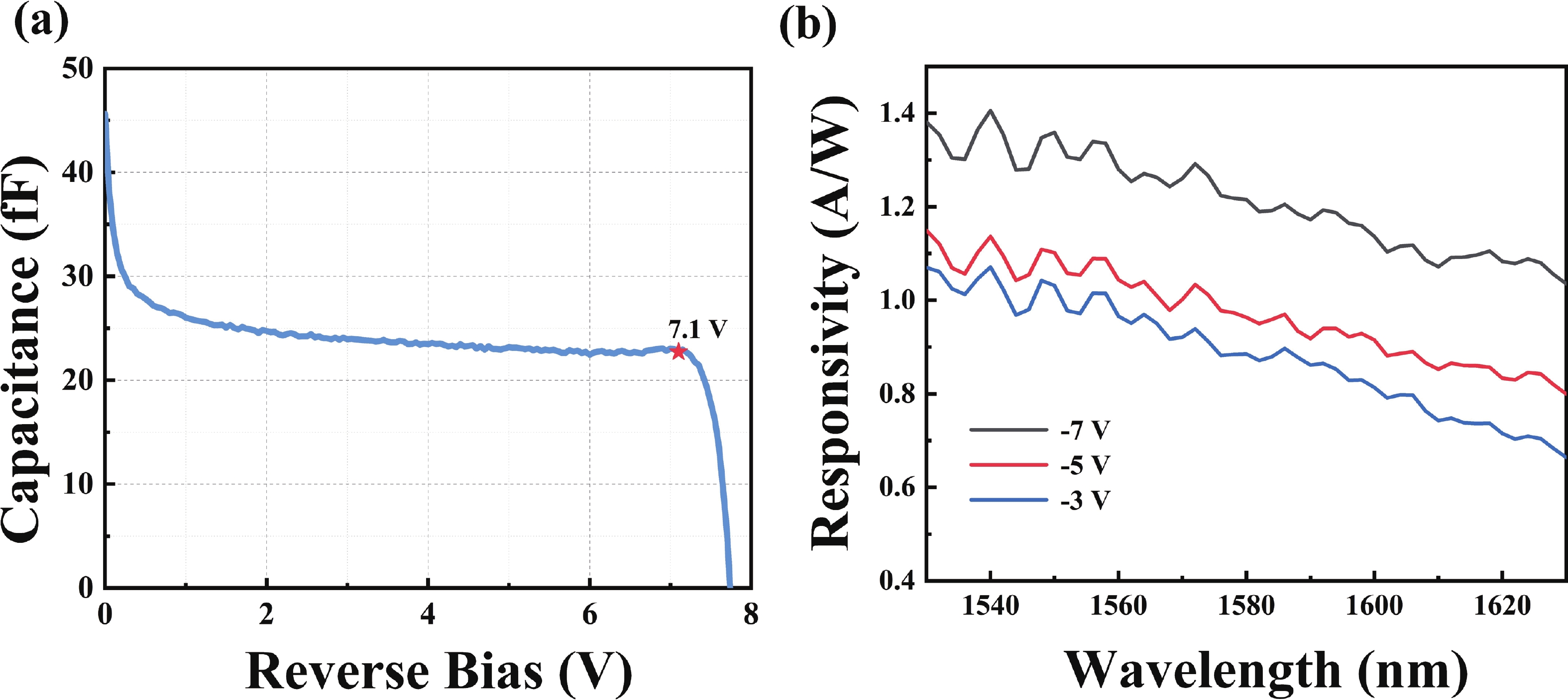
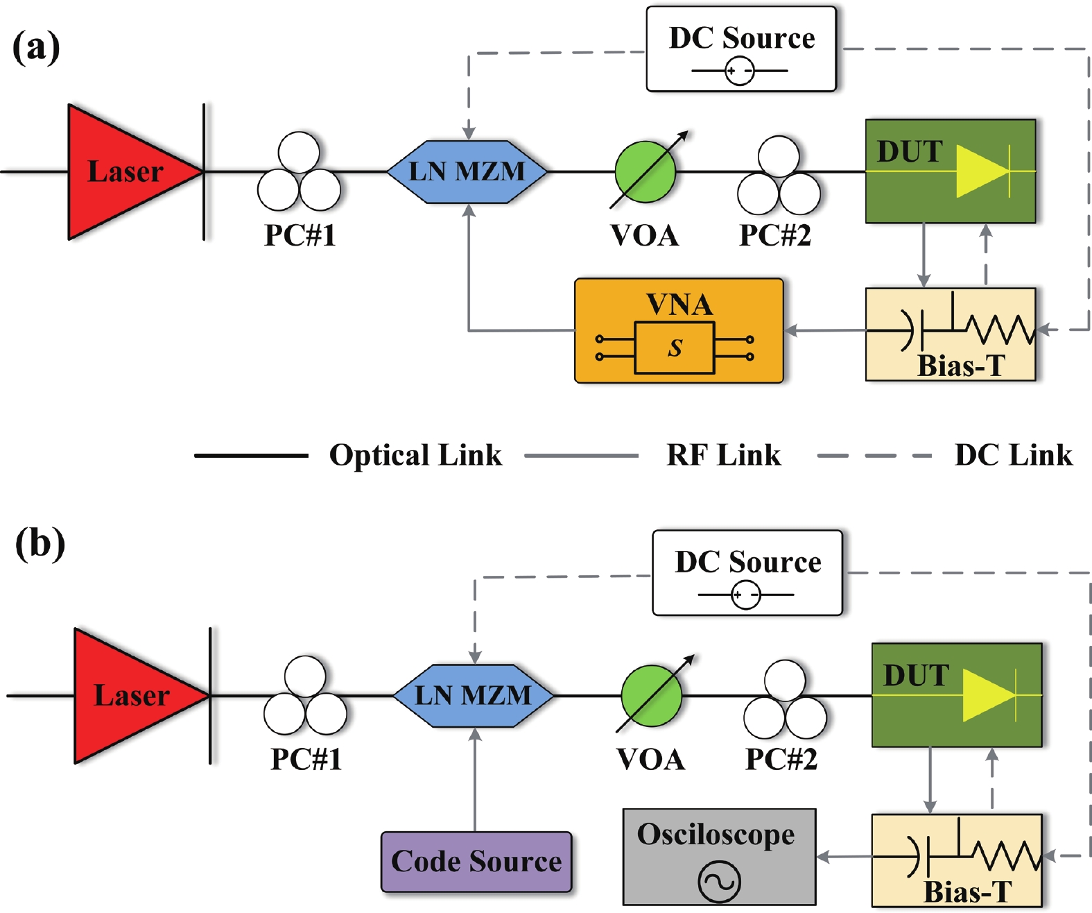
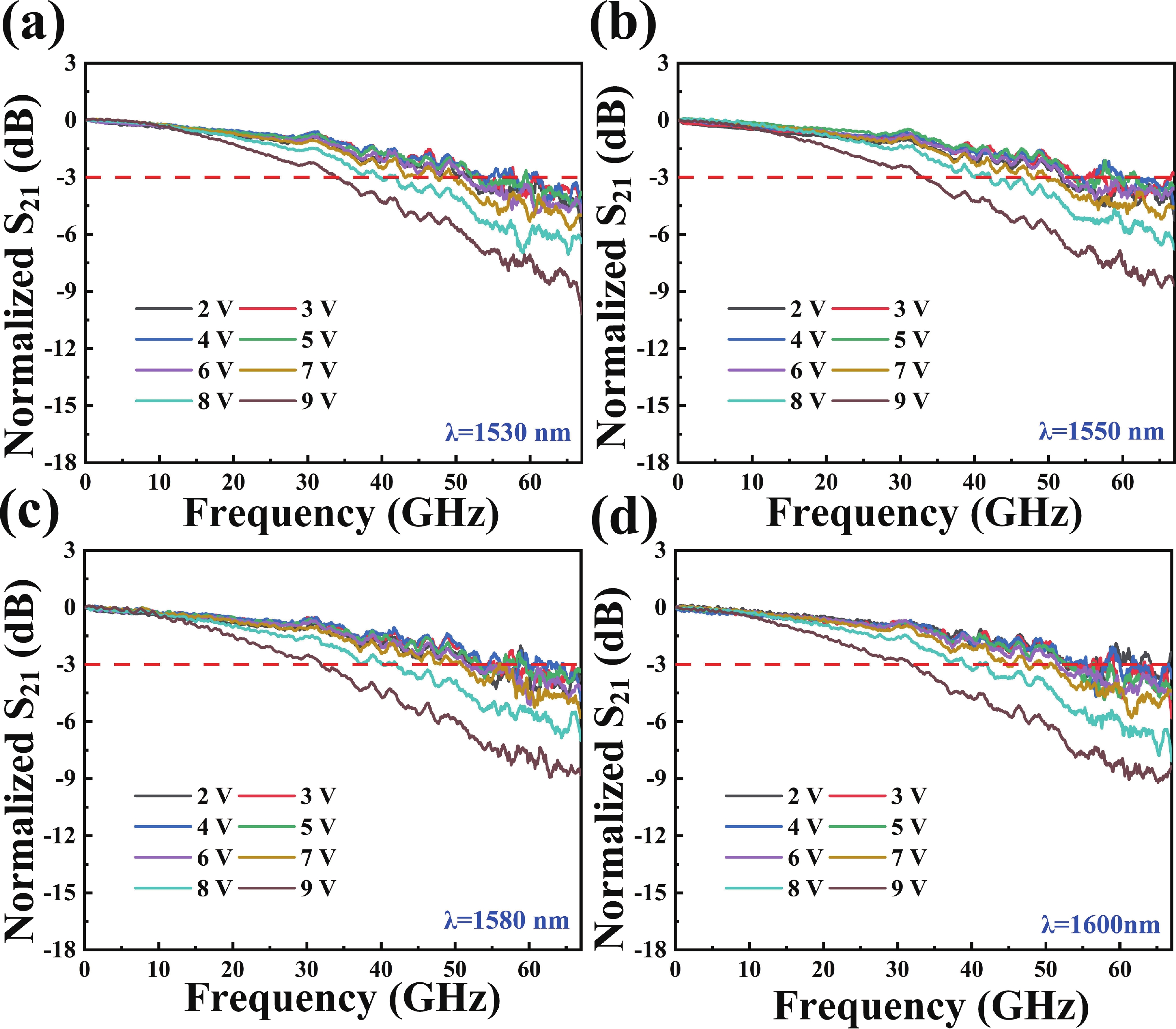
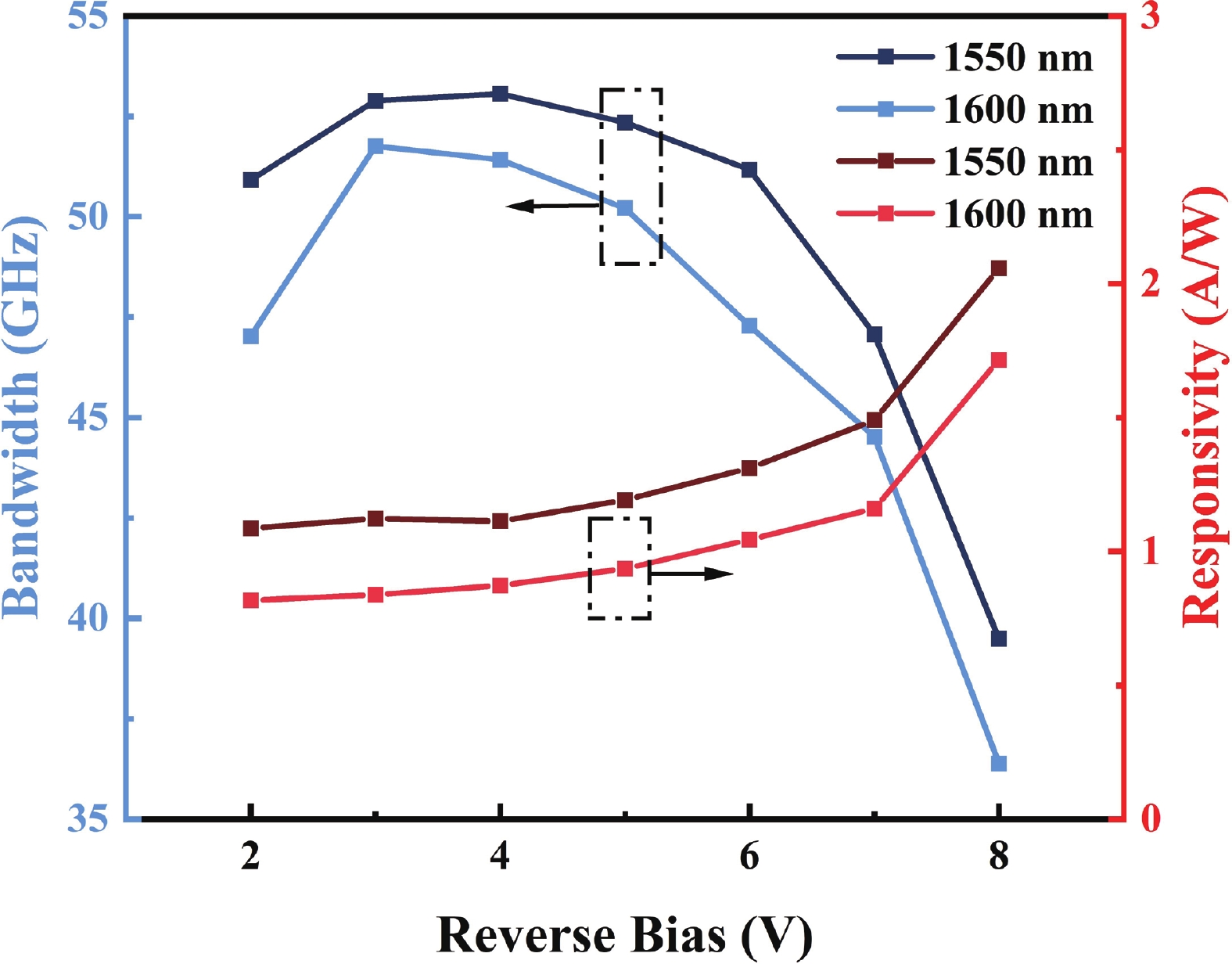
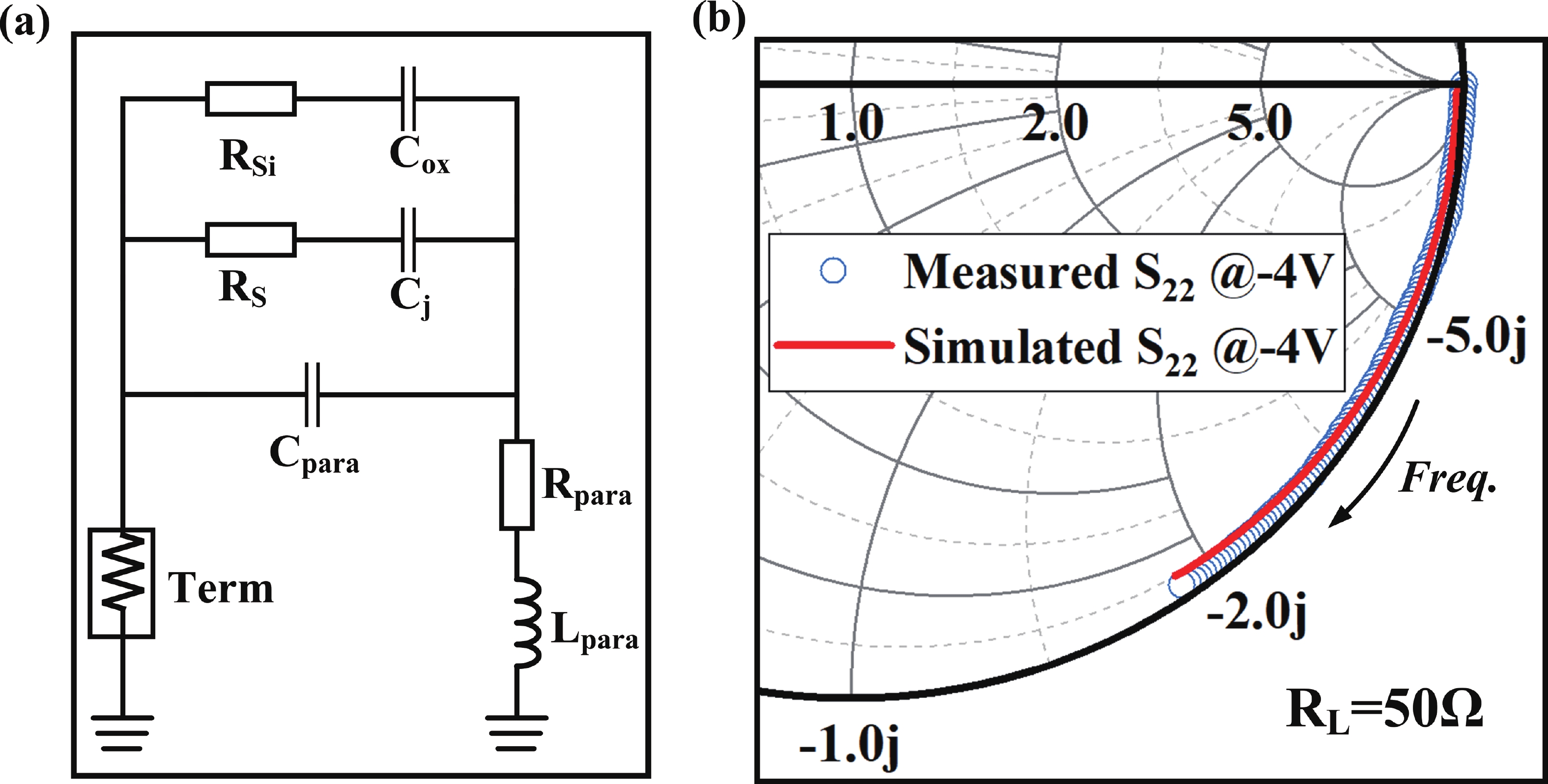
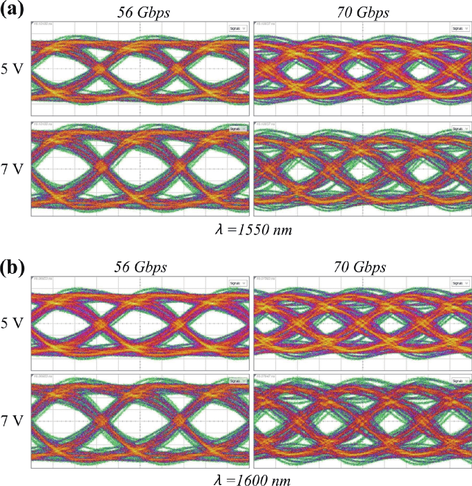
A silicon-based germanium (Ge) photodetector working for C and L bands is proposed in this paper. The device features a novel asymmetric PIN structure, which contributes to a more optimized electric field distribution in Ge and a shorter effective width of depleted region. Meanwhile, the optical structure is designed carefully to enhance responsivity for broadband. Under −7 V, where the weak avalanche process happens, the responsivity of our device is 1.49 and 1.16 A/W at 1550 and 1600 nm, with bandwidth of 47.1 and 44.5 GHz, respectively. These performances demonstrate the significant application potential of the device in optical communication systems.
J. Semicond.
2025, 46(10): 102501 doi: 10.1088/1674-4926/25020024
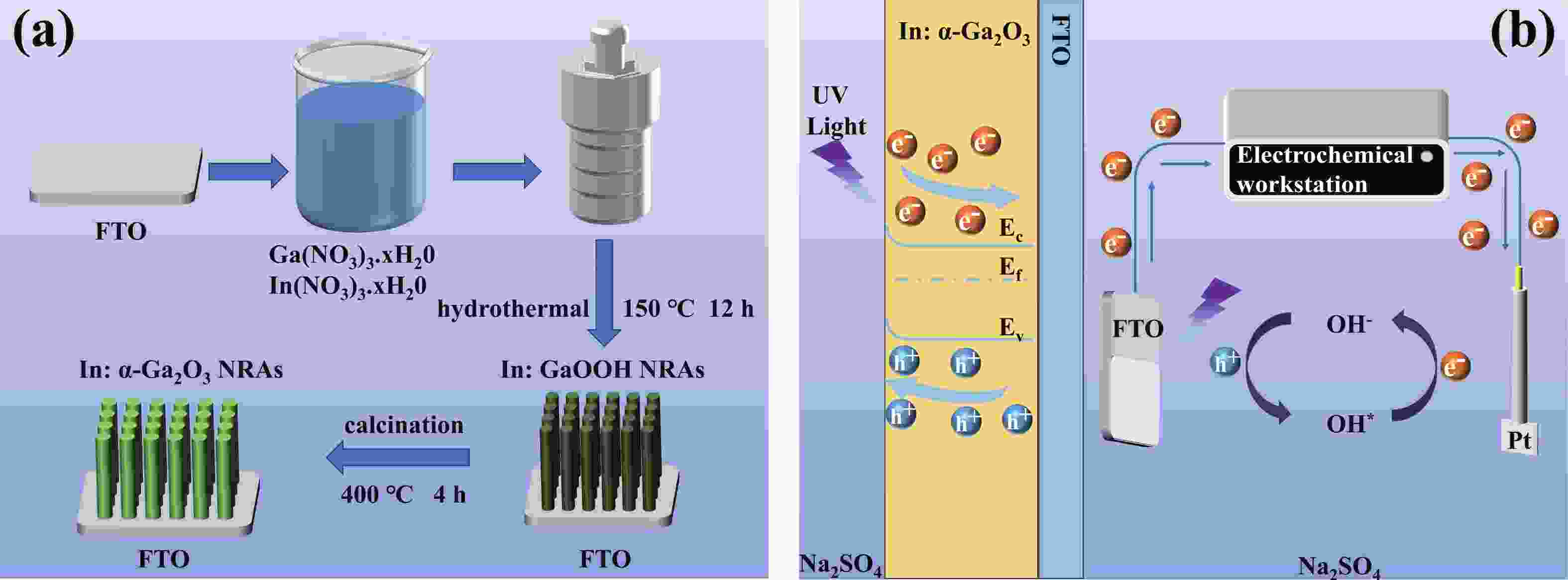
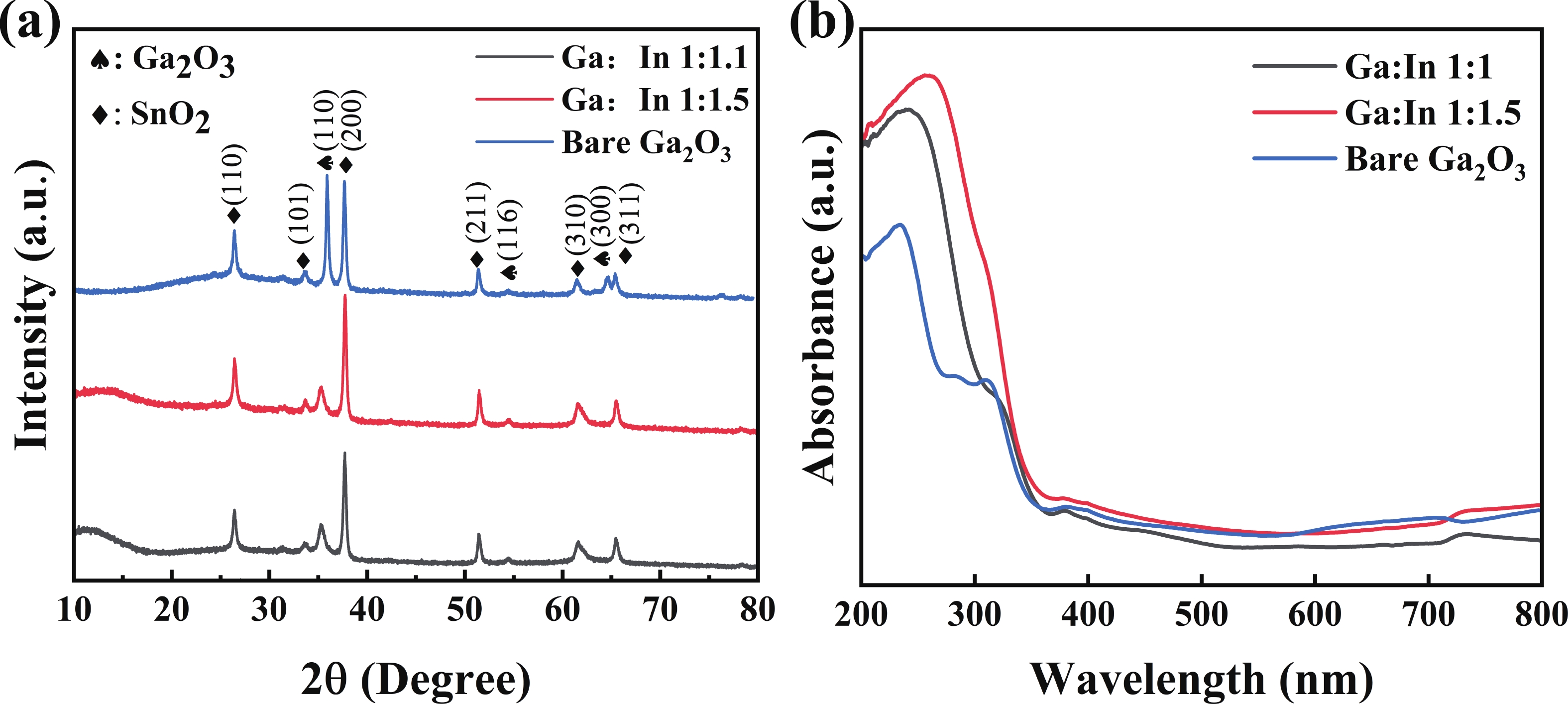
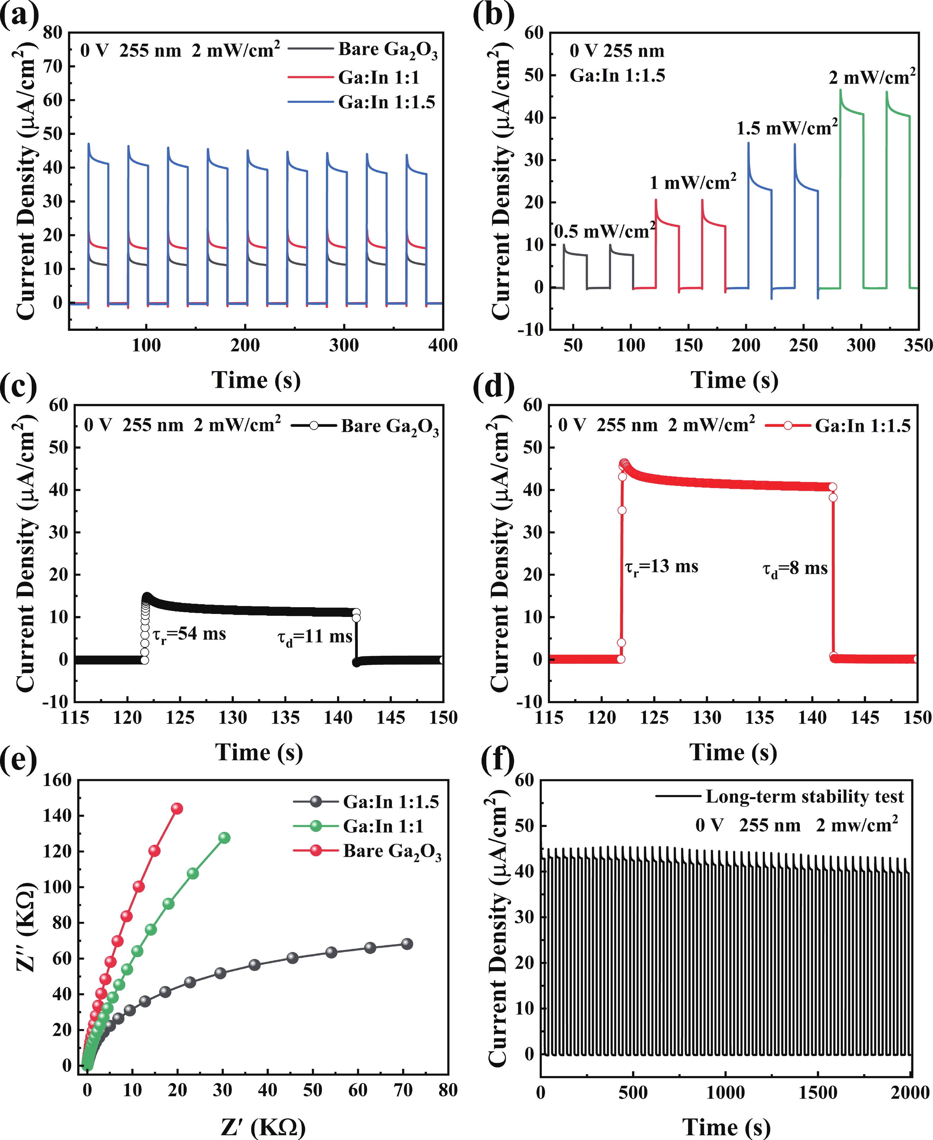
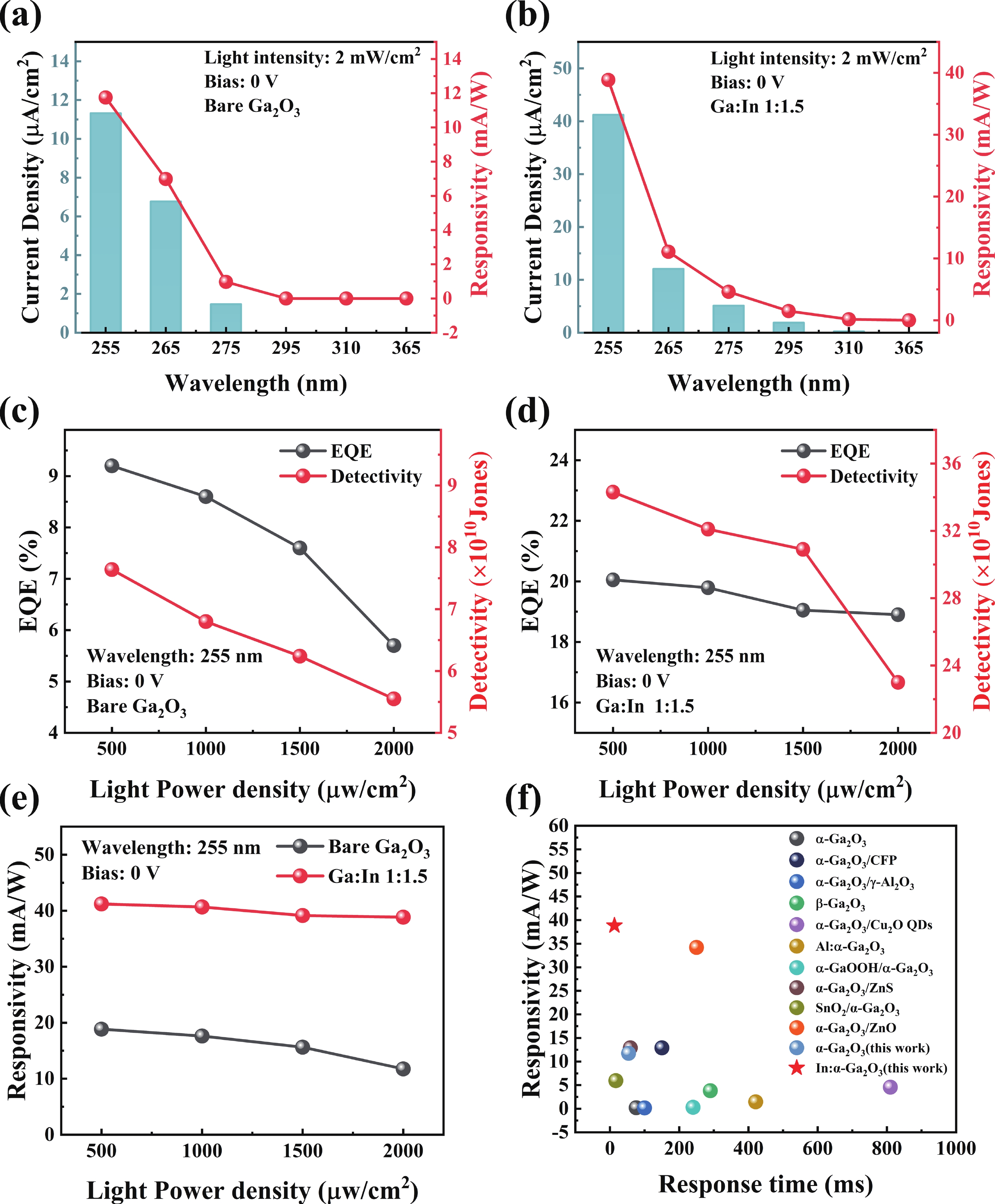
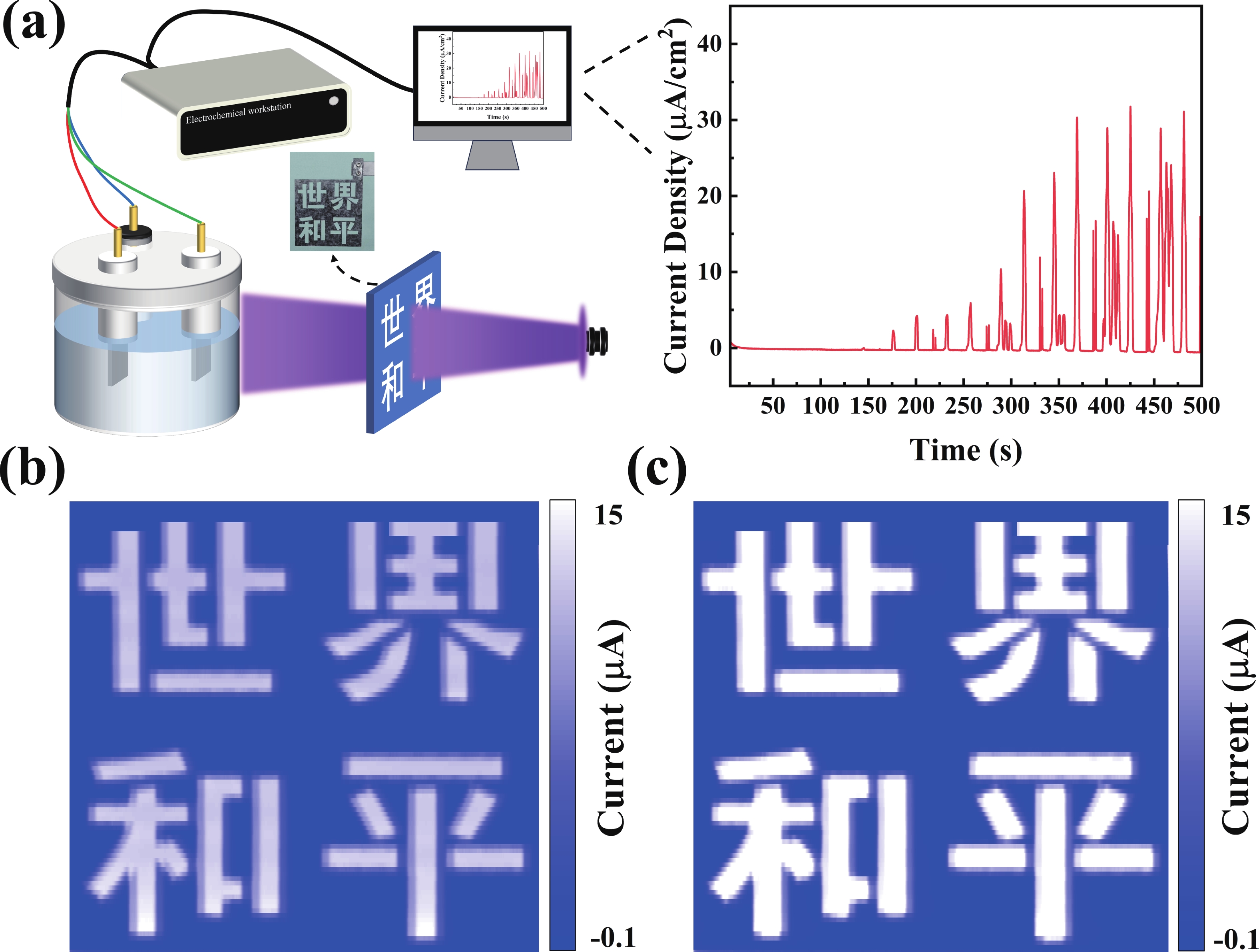
Low power consumption, high responsivity, and self-powering are key objectives for photoelectrochemical ultraviolet detectors. In this research, In-doped α-Ga2O3 nanowire arrays were fabricated on fluorine-doped tin oxide (FTO) substrates through a hydrothermal approach, with subsequent thermal annealing. These arrays were then used as photoanodes to construct a ultraviolet (UV) photodetector. In doping reduced the bandgap of α-Ga2O3, enhancing its absorption of UV light. Consequently, the In-doped α-Ga2O3 nanowire arrays exhibited excellent light detection performance. When irradiated by 255 nm deep ultraviolet light, they obtained a responsivity of 38.85 mA/W. Moreover, the detector's response and recovery times are 13 and 8 ms, respectively. The In-doped α-Ga2O3 nanowire arrays exhibit a responsivity that is about three-fold higher than the undoped one. Due to its superior responsivity, the In-doped device was used to develop a photoelectric imaging system. This study demonstrates that doping α-Ga2O3 nanowire with indium is a potent approach for optimizing their photoelectrochemical performance, which also has significant potential for optoelectronic applications.
J. Semicond.
2025, 46(10): 102601 doi: 10.1088/1674-4926/25020029
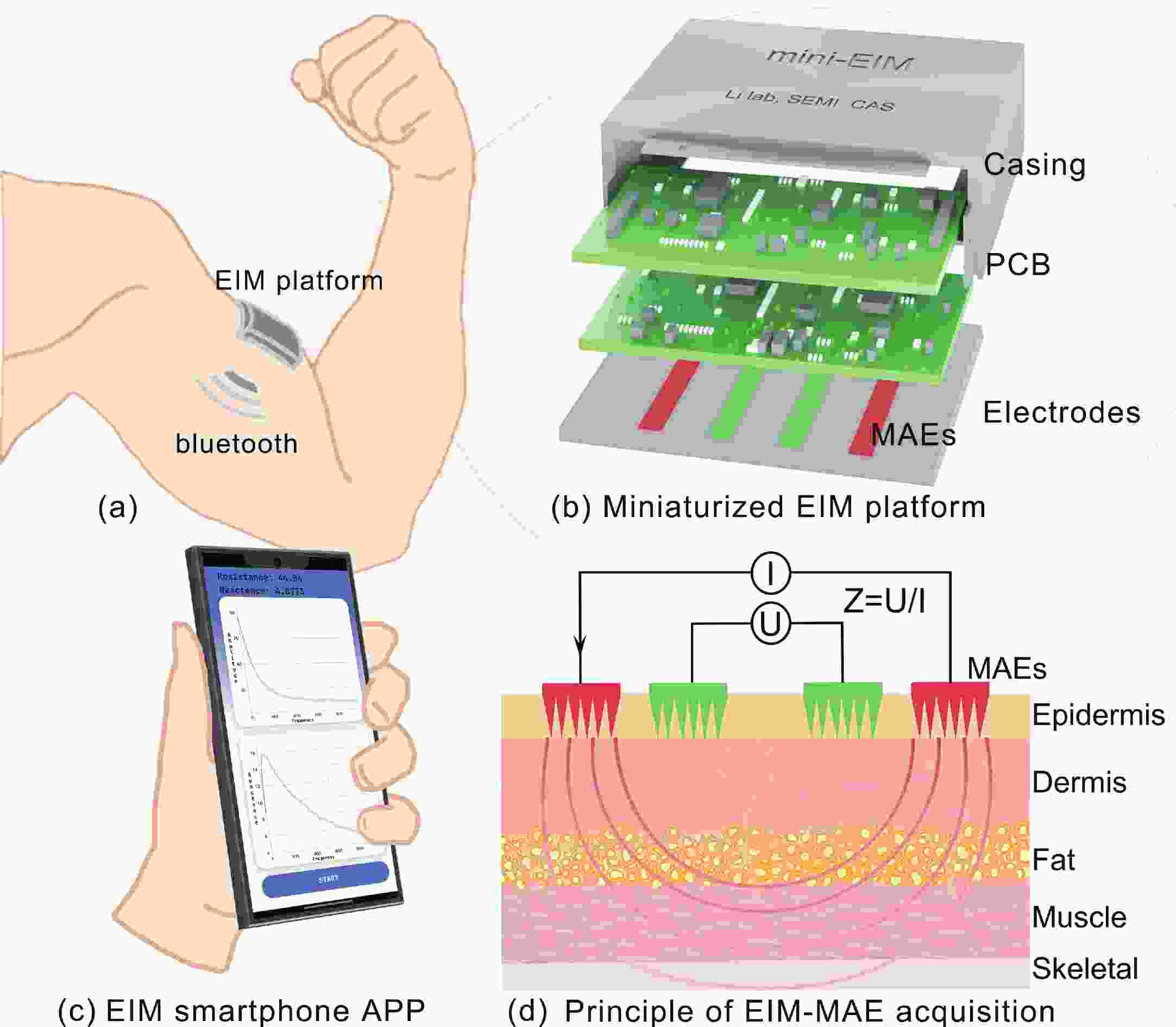
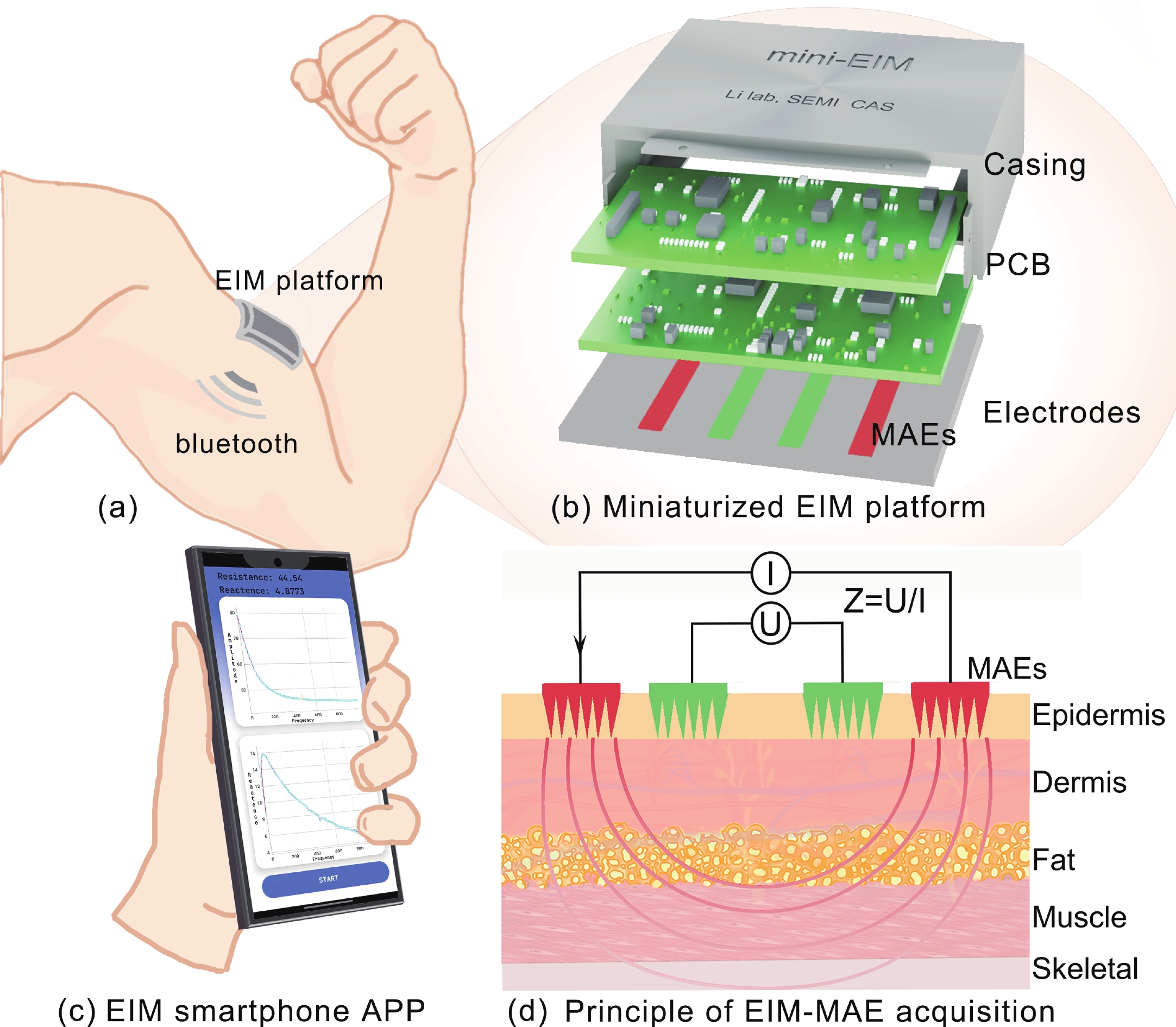
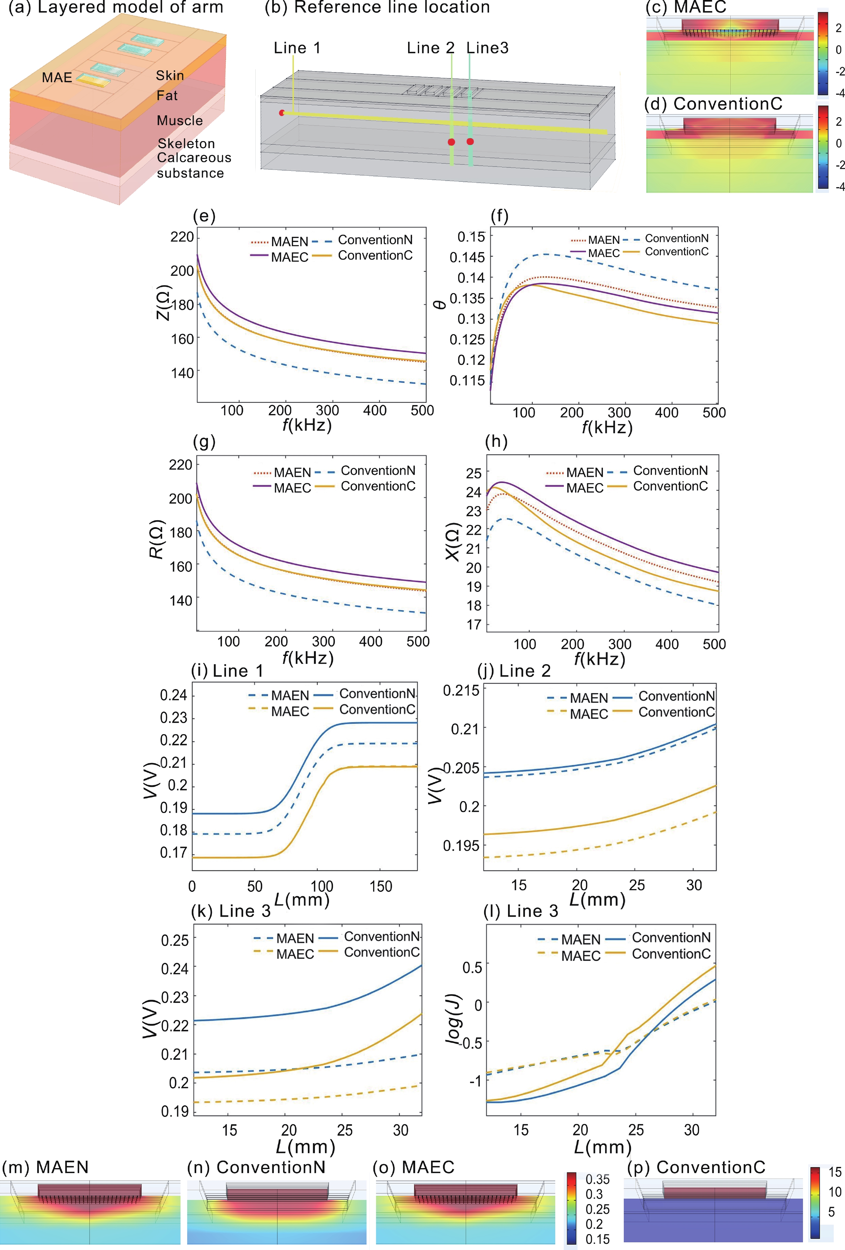
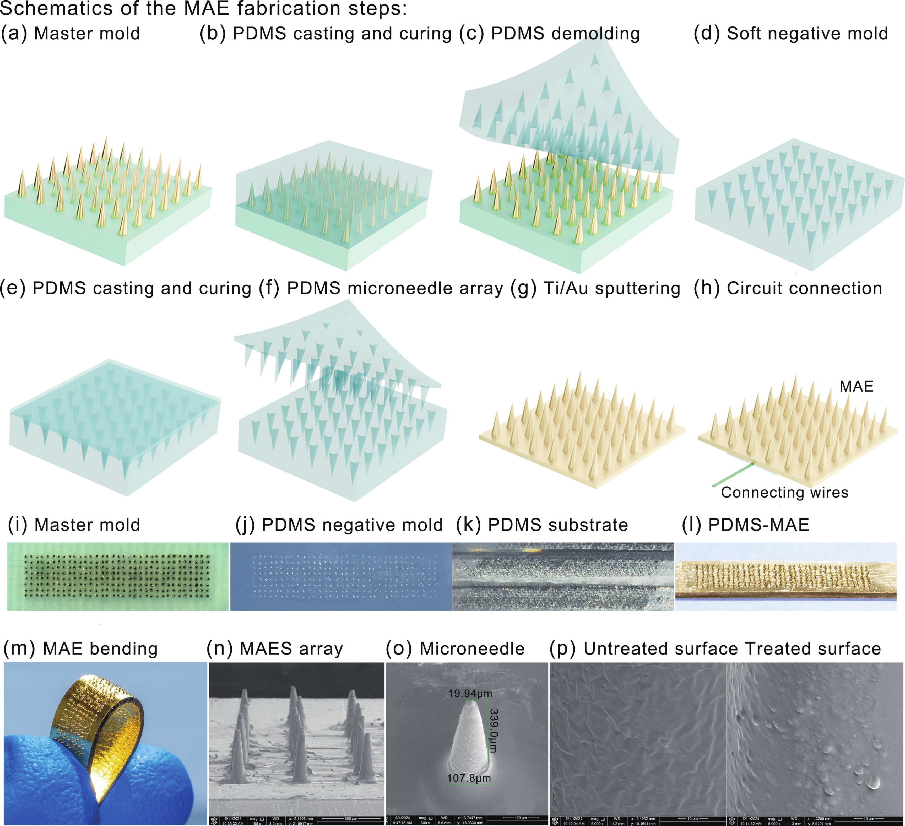
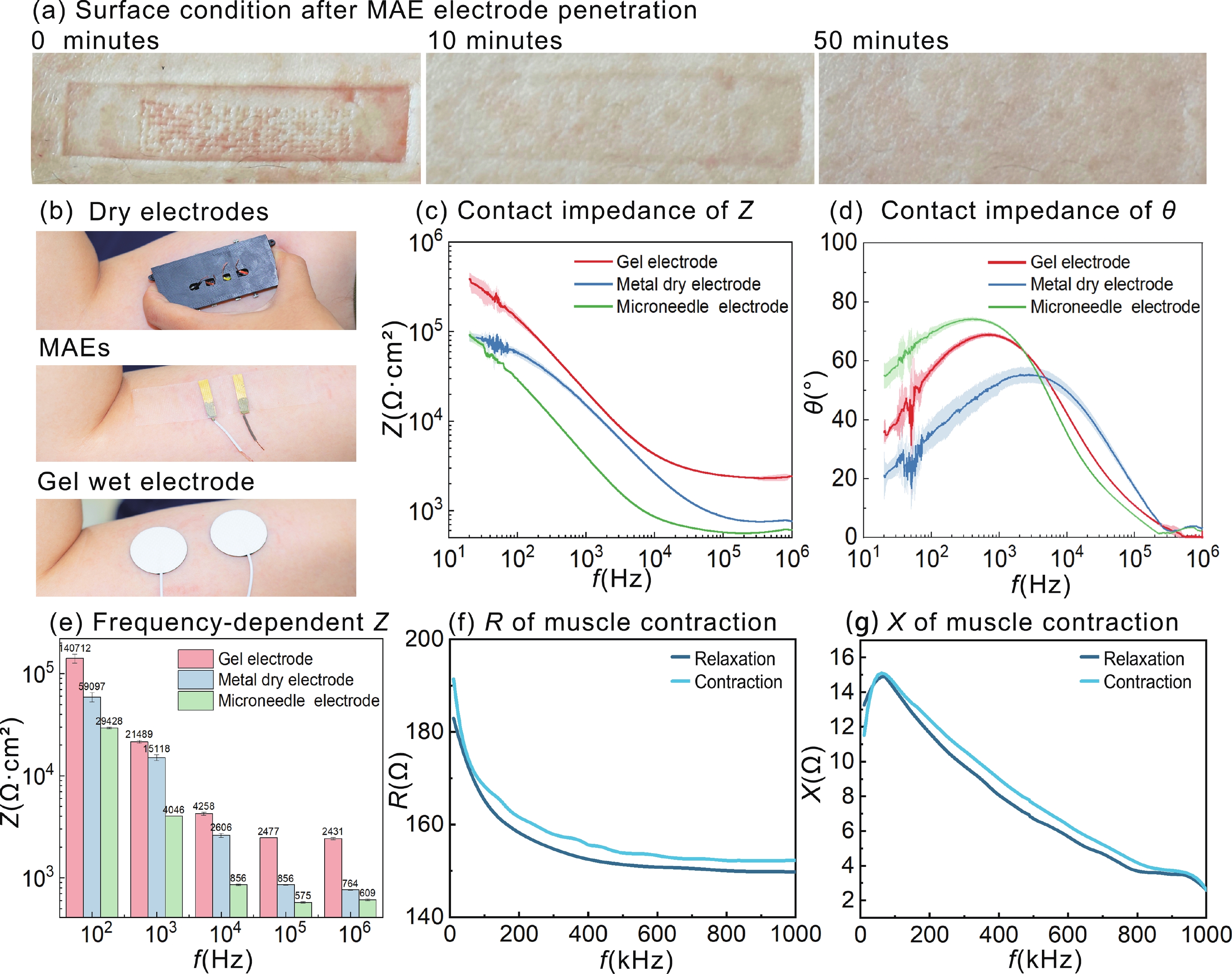
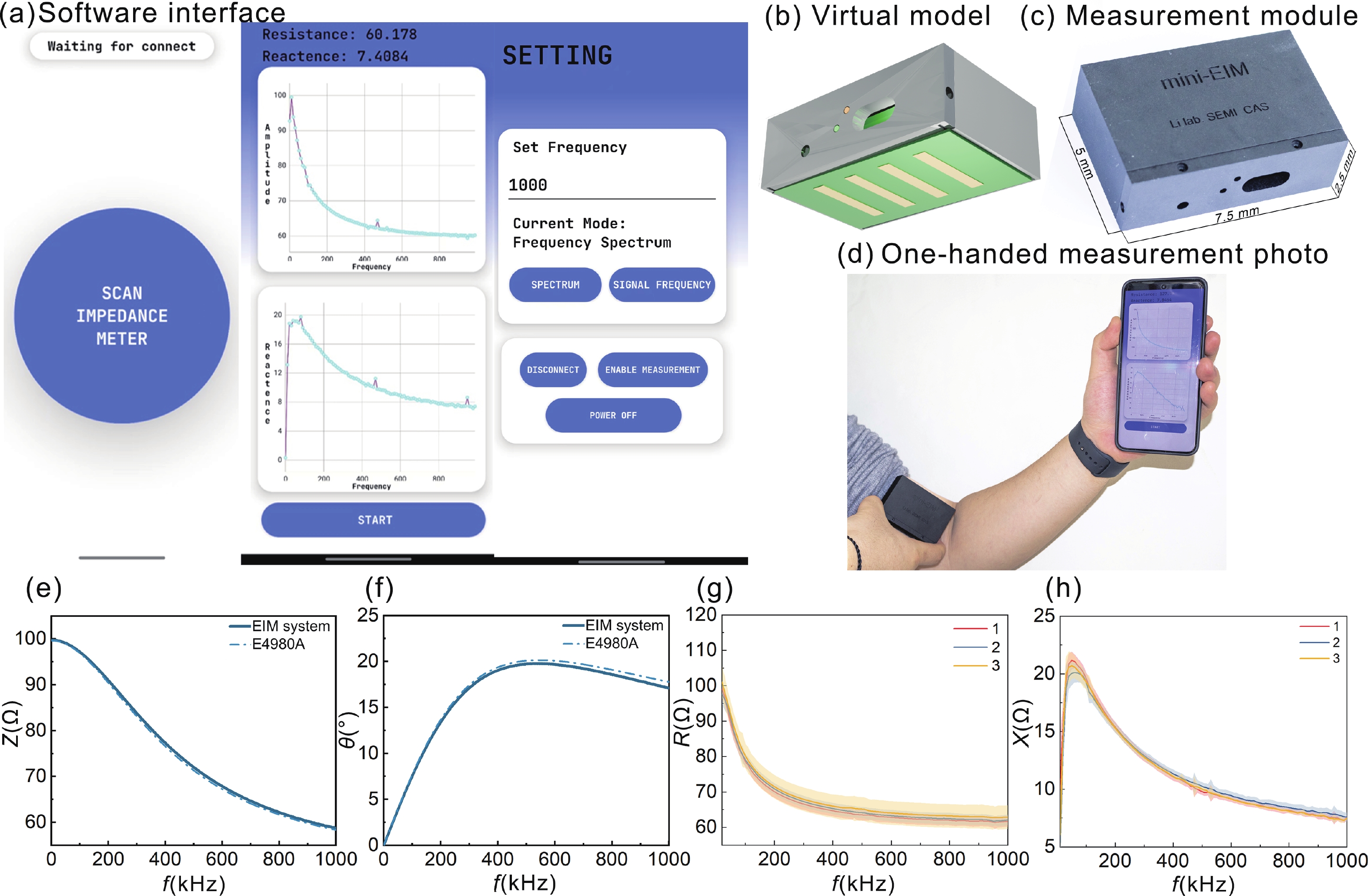
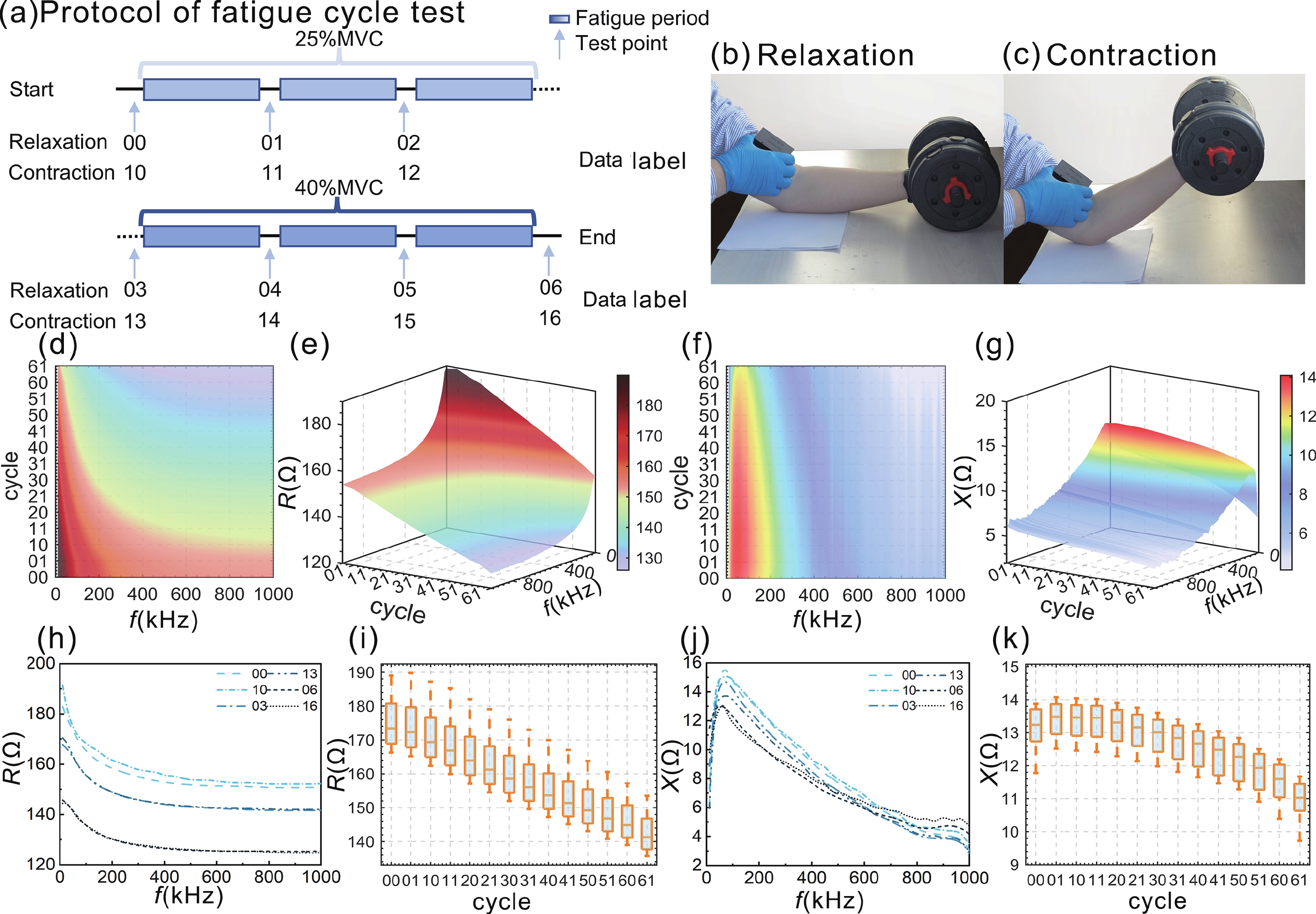
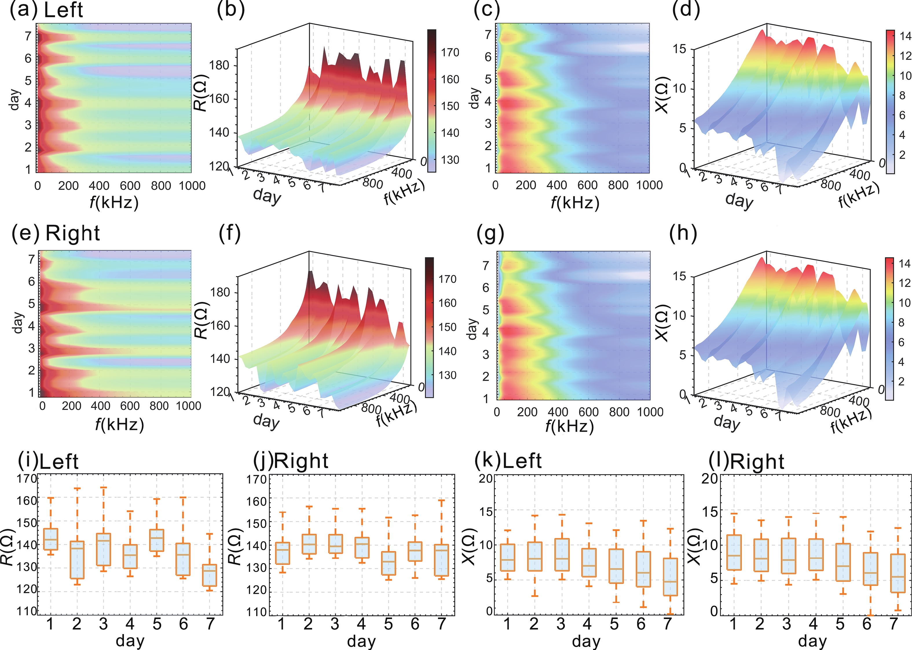
Accurate quantification of exercise interventions and changes in muscle function is essential for personalized health management. Electrical impedance myography (EIM) technology offers an innovative, noninvasive, painless, and easy-to-perform solution for muscle health monitoring. However, current EIM platforms face a number of limitations, including large device size, wired connections, and instability of the electrode-skin interface, which limit their applicability for monitoring muscle movement. In this study, a miniature wireless EIM platform with a user-friendly smartphone app is proposed and developed. The miniature, wireless, multi-frequency (20 kHz−1 MHz) EIM platform is equipped with flexible microneedle array electrodes (MAE). The advantages of MAEs over conventional electrodes were demonstrated by physical field modeling simulations and skin-electrode contact impedance comparison tests. The smartphone APP was developed to wirelessly operate the EIM platform, and to transmit and process real-time muscle impedance data. To validate its effectiveness, a seven-day adaptive fatigue training study was conducted, which demonstrated that the EIM platform was able to detect muscle adaptations and serve as a reliable indicator of fatigue. This study presents an innovative approach to applying EIM technology to muscle health monitoring and exercise testing, thereby advancing the development of personalized health management and athletic performance assessment.
J. Semicond.
2025, 46(10): 102801 doi: 10.1088/1674-4926/25010022
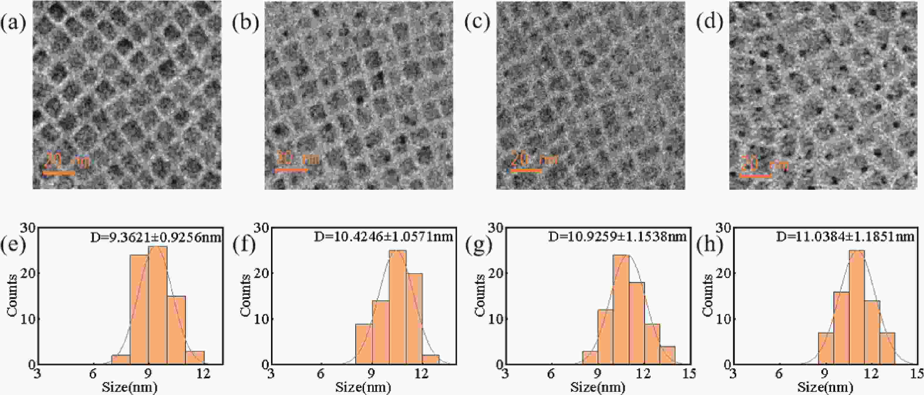
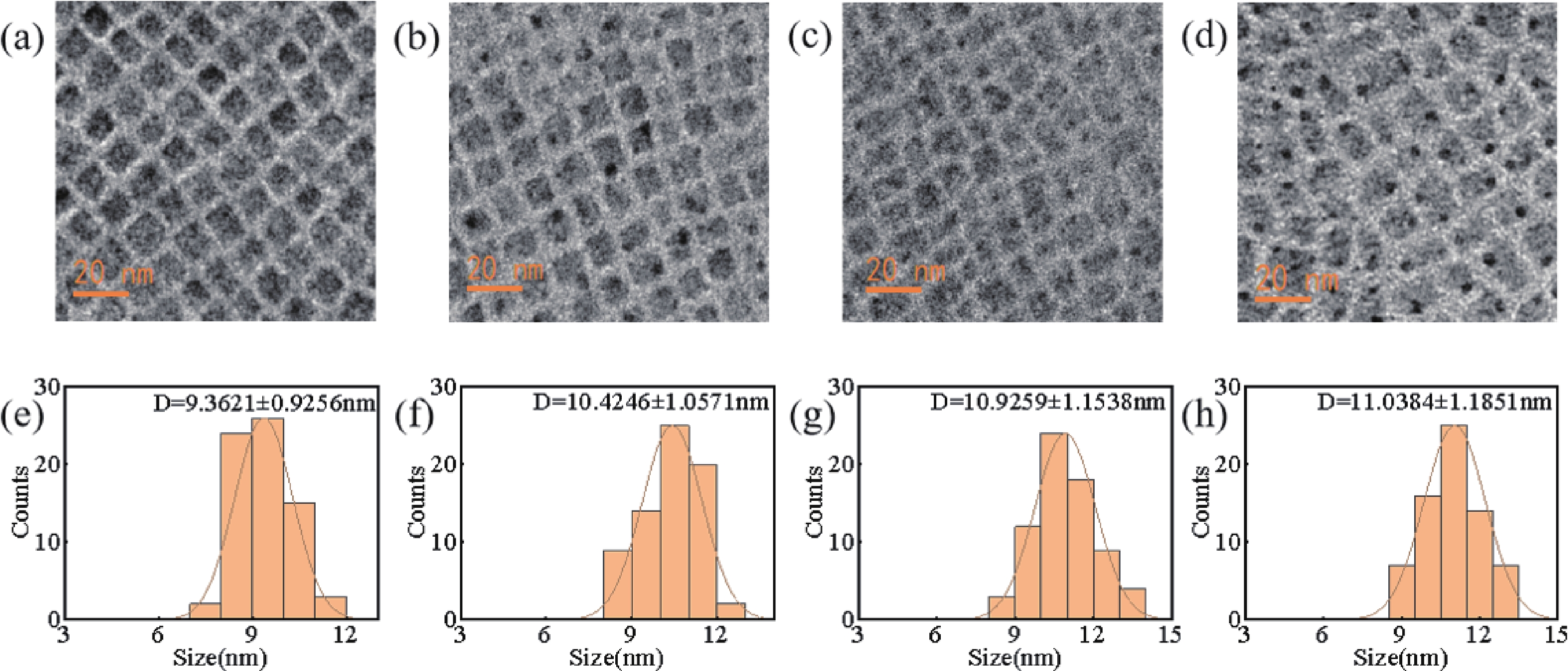
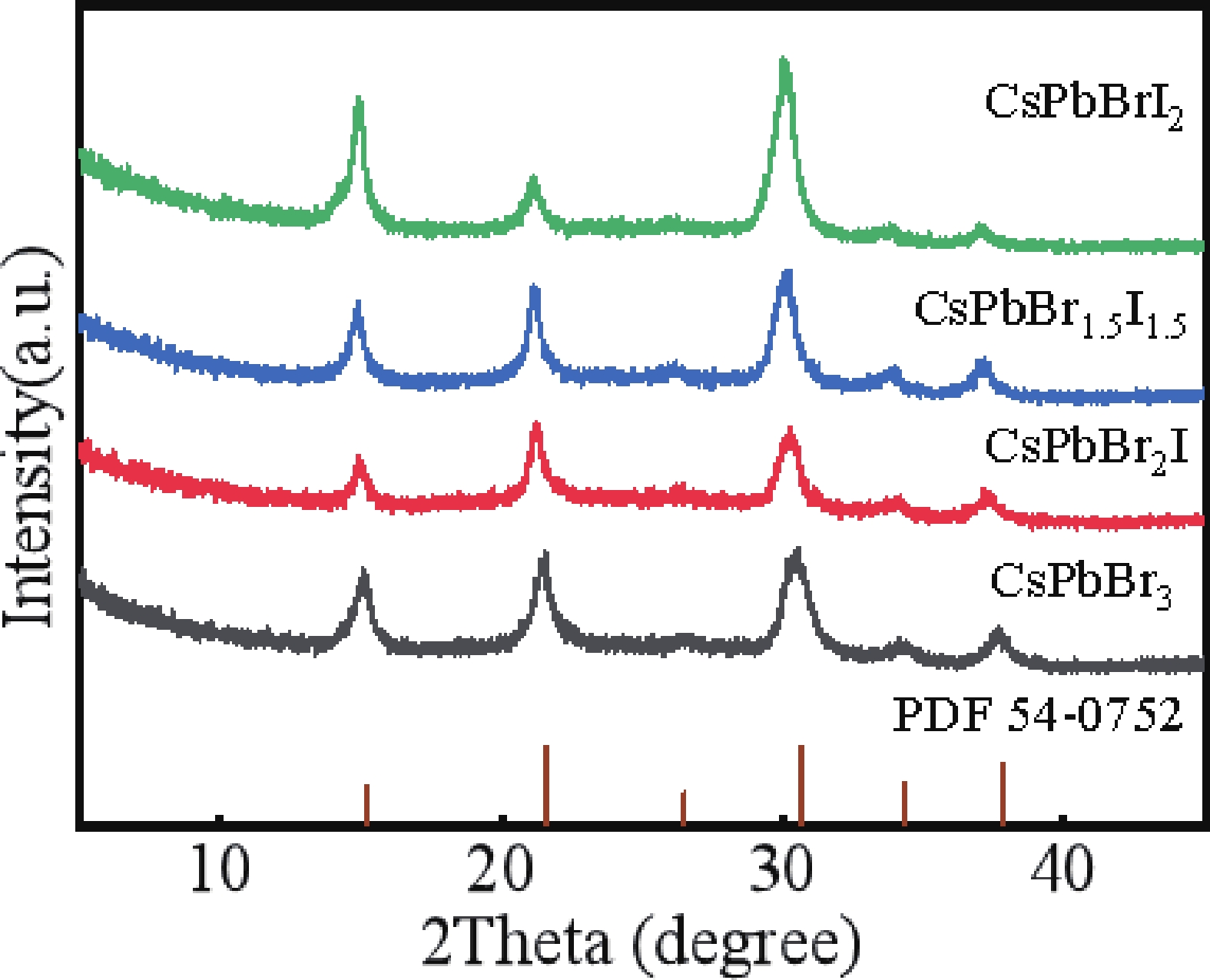
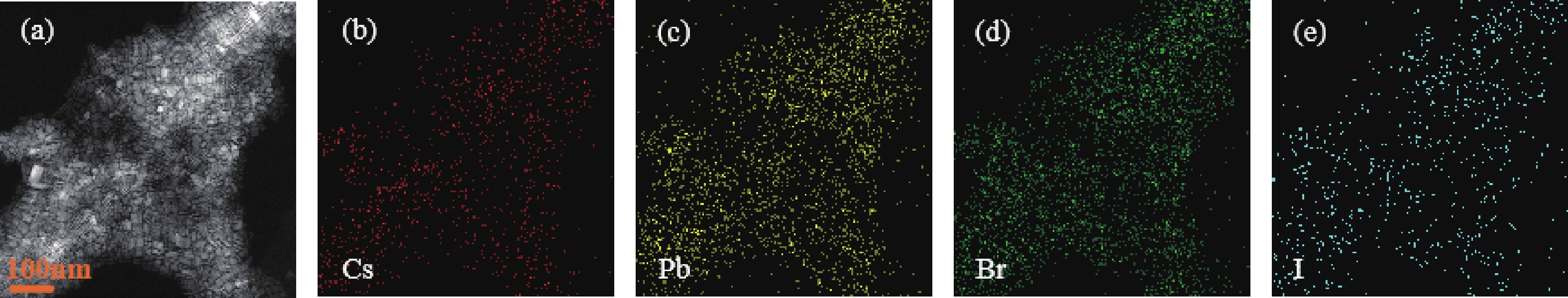
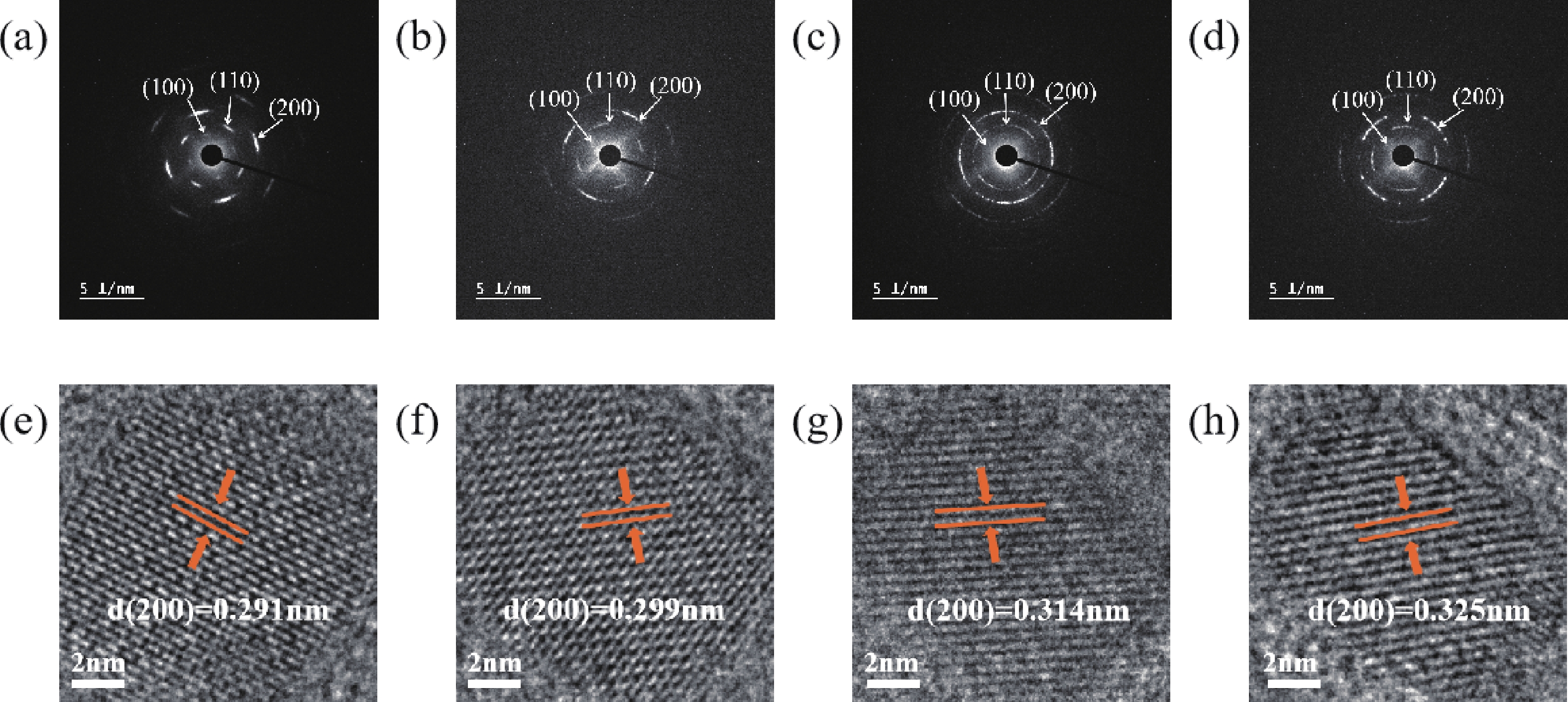
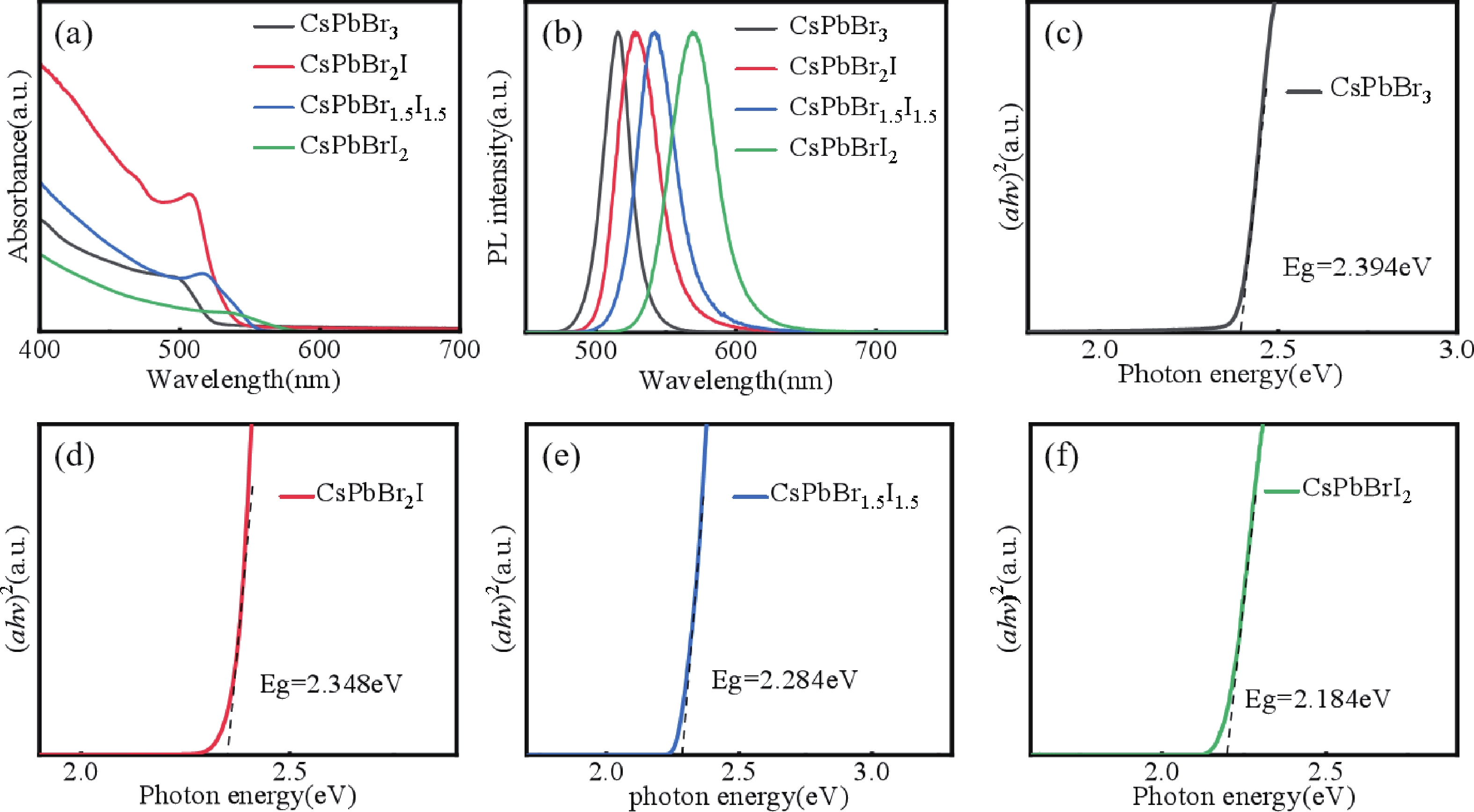
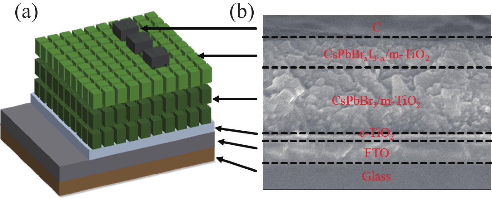
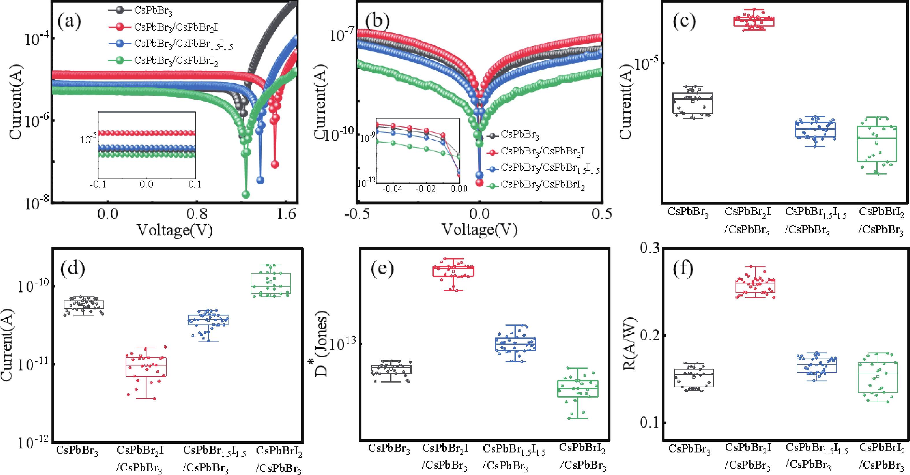
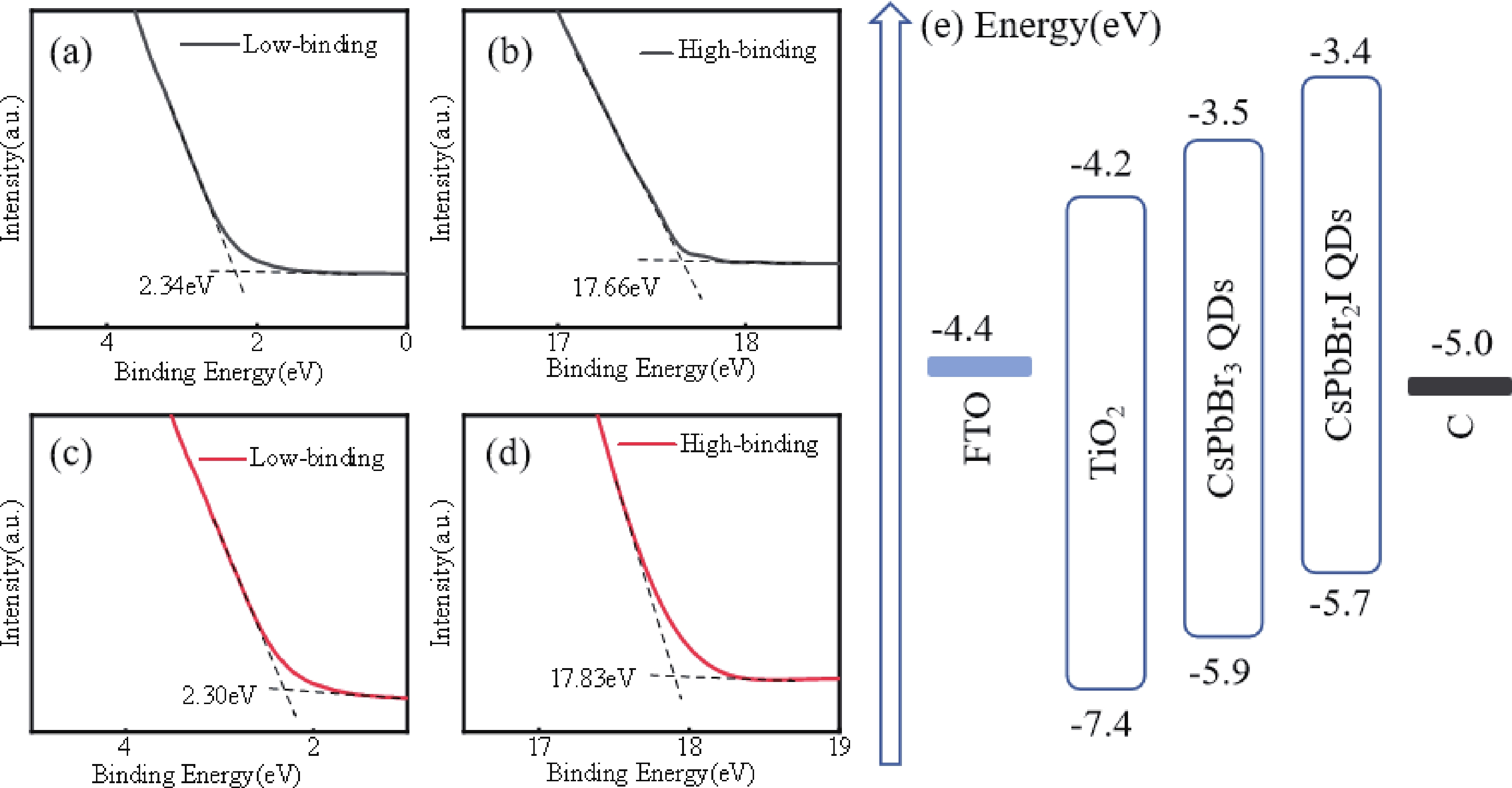
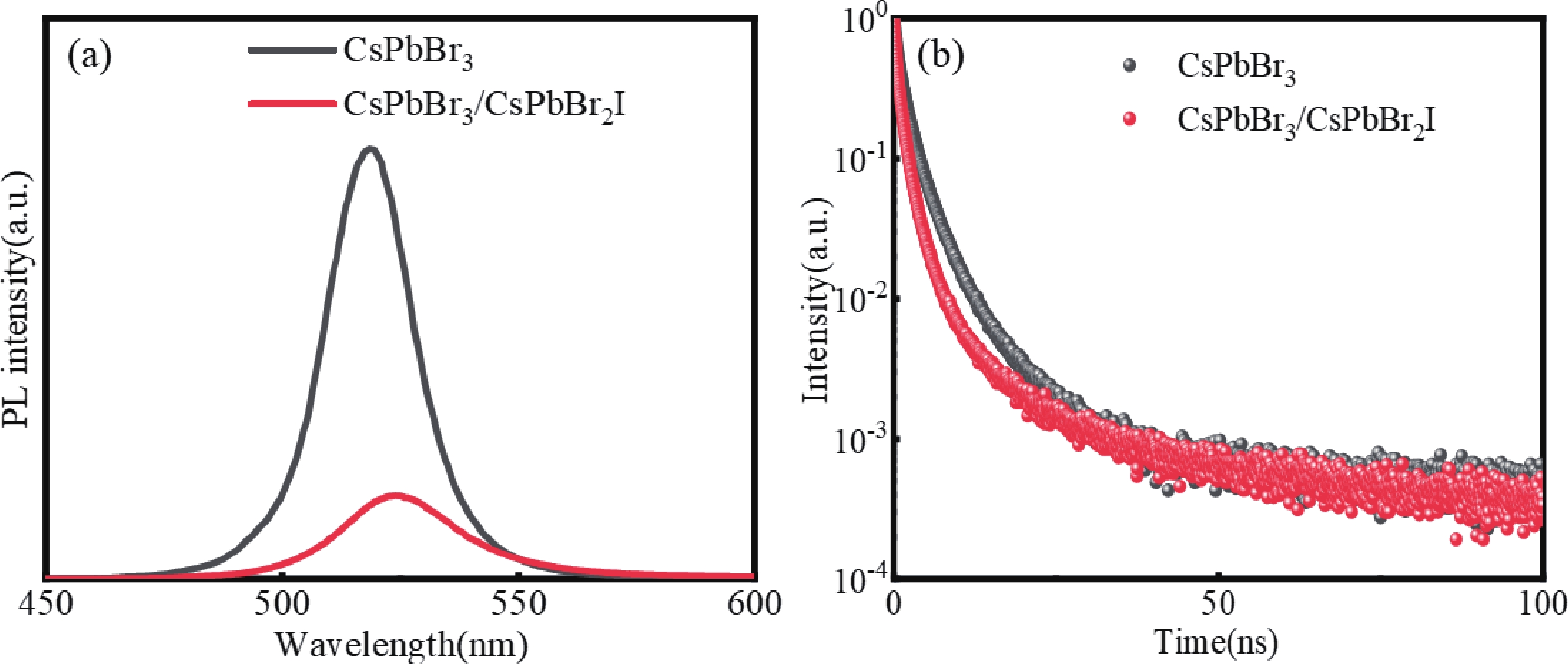
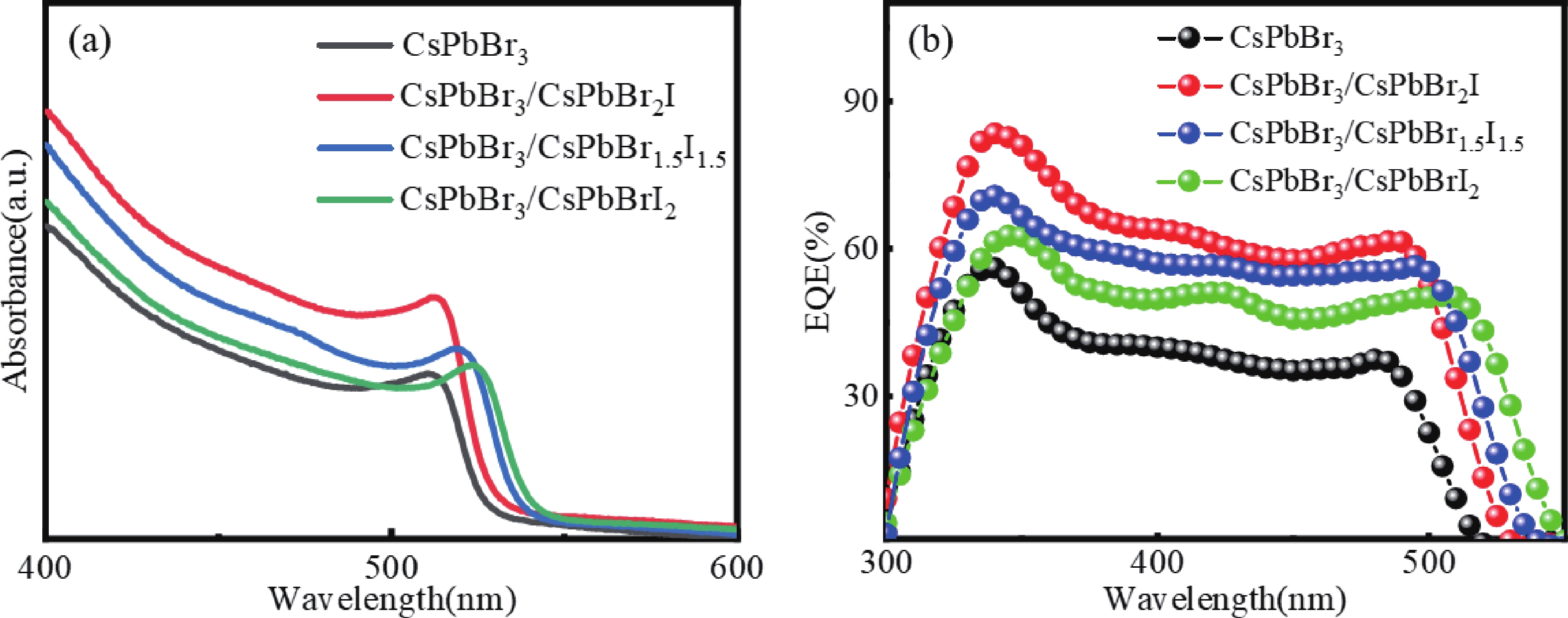
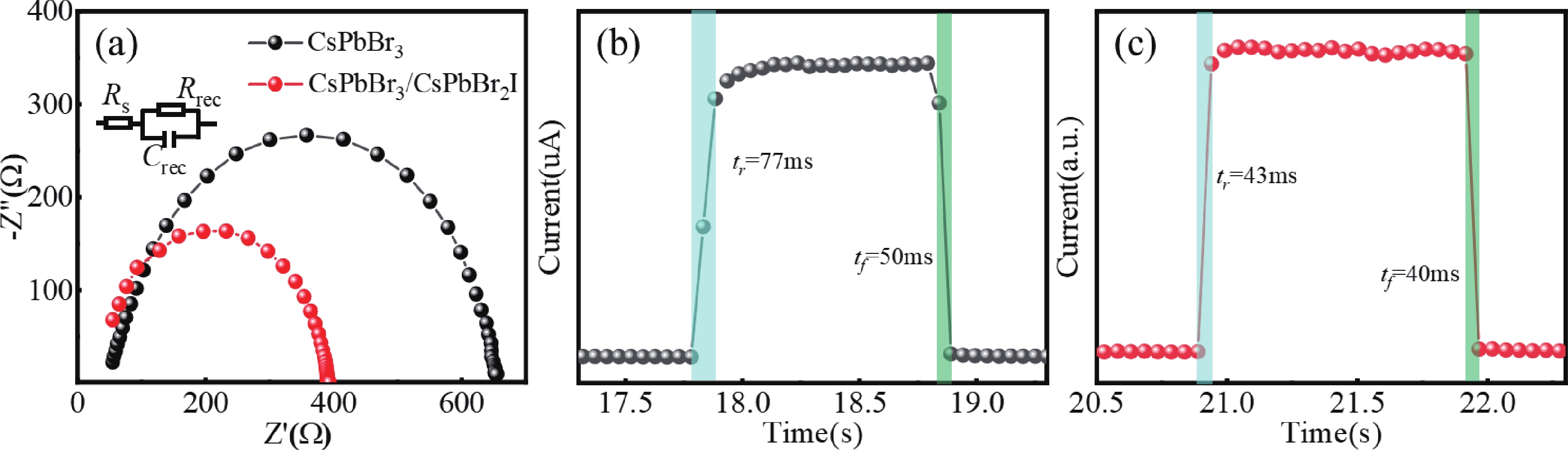
All-inorganic CsPbBr3 perovskite quantum dots (QDs) have attracted extensive attention in photoelectric detection for their excellent photoelectric properties and stability. However, the CsPbBr3 quantum dot film exhibits a high non-radiative recombination rate, and the mismatch in energy levels with the carbon electrode weakens hole extraction efficiency. These reduces the device's performance. To improve this, a semiconductor photodetector based on fluorine-doped tin oxide (FTO)/dense titanium dioxide (c-TiO2)/mesoporous titanium dioxide (m-TiO2)/CsPbBr3 QDs/CsPbBrxI3–x (x = 2, 1.5, 1) QDs/C structure was studied. By adjusting the Br– : I– ratio, the synthesized CsPbBrxI3–x (x = 2, 1.5, 1) QDs showed an adjustable band gap width of 2.284−2.394 eV. And forming a type Ⅱ band structure with CsPbBr3 QDs, which reduced the valence band offset between the active layer and the carbon electrode, this promoted carrier extraction and reduced non-radiative recombination rate. Compared with the original device (the photosensitive layer is CsPbBr3 QDs), the performance of the photodetector based on the CsPbBr3 QDs/CsPbBr2I QDs heterostructure is significantly improved, the responsivity (R) increased by 73%, the specific detectivity rate (D*) increased from 6.98 × 10¹² to 3.19 × 10¹³ Jones, the on/off ratio reached 106. This study provides a new idea for the development of semiconductor tandem detectors.