


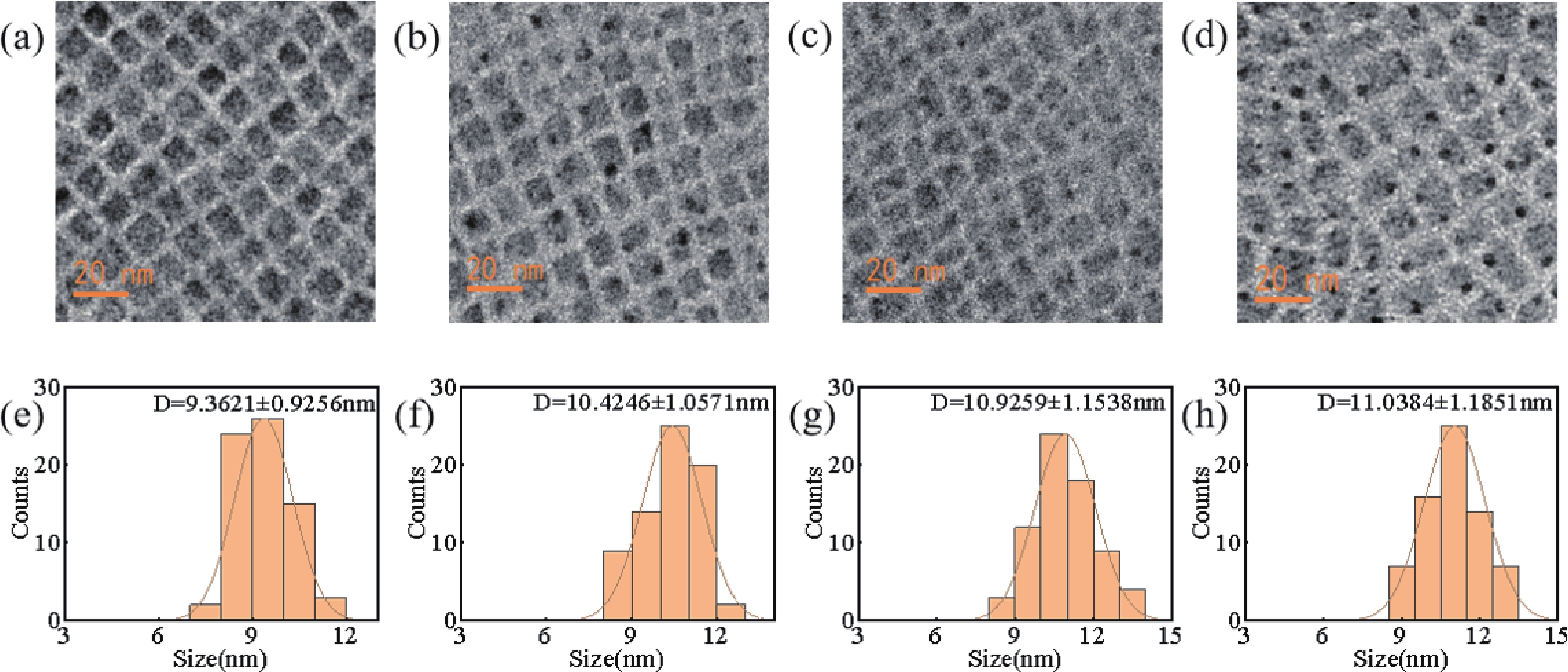
Fig. 1.
(Color online) (a)–(d) The TEM images of CsPbBrxI3–x QDs (x = 3, 2, 1.5, 1), respectively. The particle size distribution histograms of CsPbBrxI3–x (x = 3, 2, 1.5, 1) QDs were represented by (e)–(h).
ARTICLES
Chenguang Shen, Mengwei Chen, Wei Huang and Yingping Yang
Corresponding author: Mengwei Chen, mengwei.chen@whut.edu.cn; Yingping Yang, ypyang@whut.edu.cn
Abstract: All-inorganic CsPbBr3 perovskite quantum dots (QDs) have attracted extensive attention in photoelectric detection for their excellent photoelectric properties and stability. However, the CsPbBr3 quantum dot film exhibits a high non-radiative recombination rate, and the mismatch in energy levels with the carbon electrode weakens hole extraction efficiency. These reduces the device's performance. To improve this, a semiconductor photodetector based on fluorine-doped tin oxide (FTO)/dense titanium dioxide (c-TiO2)/mesoporous titanium dioxide (m-TiO2)/CsPbBr3 QDs/CsPbBrxI3–x (x = 2, 1.5, 1) QDs/C structure was studied. By adjusting the Br– : I– ratio, the synthesized CsPbBrxI3–x (x = 2, 1.5, 1) QDs showed an adjustable band gap width of 2.284−2.394 eV. And forming a type Ⅱ band structure with CsPbBr3 QDs, which reduced the valence band offset between the active layer and the carbon electrode, this promoted carrier extraction and reduced non-radiative recombination rate. Compared with the original device (the photosensitive layer is CsPbBr3 QDs), the performance of the photodetector based on the CsPbBr3 QDs/CsPbBr2I QDs heterostructure is significantly improved, the responsivity (R) increased by 73%, the specific detectivity rate (D*) increased from 6.98 × 10¹² to 3.19 × 10¹³ Jones, the on/off ratio reached 106. This study provides a new idea for the development of semiconductor tandem detectors.
Keywords: photodetector, all-inorganic perovskite, quantum dots, semiconductor, heterostructure
| [1] |
Yadav S N S, Hanmandlu C, Patel D K, et al. Enhanced photoresponsivity of perovskite QDs/graphene hybrid gate-free photodetector by morphologically controlled plasmonic Au nanocrystals. Adv Opt Mater, 2023, 11(15), 2300131 doi: 10.1002/adom.202300131
|
| [2] |
Liu D, Yin Y X, Liu F J, et al. Thickness-dependent highly sensitive photodetection behavior of lead-free all-inorganic CsSnBr3 nanoplates. Rare Met, 2022, 41(5), 1753 doi: 10.1007/s12598-021-01909-8
|
| [3] |
Mandal A, Ghosh A, Ghosh D, et al. Photodetectors with high responsivity by thickness tunable mixed halide perovskite nanosheets. ACS Appl Mater Interfaces, 2021, 13(36), 43104 doi: 10.1021/acsami.1c13452
|
| [4] |
Chen K Q, Jin W, Zhang Y P, et al. High efficiency mesoscopic solar cells using CsPbI3 perovskite quantum dots enabled by chemical interface engineering. J Am Chem Soc, 2020, 142(8), 3775 doi: 10.1021/jacs.9b10700
|
| [5] |
Han M M, Sun J M, Peng M, et al. Controllable growth of lead-free all-inorganic perovskite nanowire array with fast and stable near-infrared photodetection. J Phys Chem C, 2019, 123(28), 17566 doi: 10.1021/acs.jpcc.9b03289
|
| [6] |
Jing H, Peng R W, Ma R M, et al. Flexible ultrathin single-crystalline perovskite photodetector. Nano Lett, 2020, 20(10), 7144 doi: 10.1021/acs.nanolett.0c02468
|
| [7] |
Popoola A, Gondal M A, Popoola I K, et al. Fabrication of bifacial sandwiched heterojunction photoconductor–Type and MAI passivated photodiode–Type perovskite photodetectors. Org Electron, 2020, 84, 105730 doi: 10.1016/j.orgel.2020.105730
|
| [8] |
Jia D L, Chen J X, Zhuang R S, et al. Antisolvent-assisted in situ cation exchange of perovskite quantum dots for efficient solar cells. Adv Mater, 2023, 35(21), e2212160 doi: 10.1002/adma.202212160
|
| [9] |
Yang Z, Xu Q, Wang X D, et al. Large and ultrastable all-inorganic CsPbBr3 monocrystalline films: Low-temperature growth and application for high-performance photodetectors. Adv Mater, 2018, 30(44), e1802110 doi: 10.1002/adma.201802110
|
| [10] |
Li J, Zhang G D, Zhang Z H, et al. Defect passivation via additive engineering to improve photodetection performance in CsPbI2Br perovskite photodetectors. ACS Appl Mater Interfaces, 2021, 13(47), 56358 doi: 10.1021/acsami.1c19323
|
| [11] |
Liu S L, Gao W Q, Chen Y, et al. Van der waals integration of large-area monocrystalline 3D perovskite thin films on arbitrary semiconductor substrates for heterojunctions. Nano Lett, 2024, 24(25), 7724 doi: 10.1021/acs.nanolett.4c01715
|
| [12] |
Zhu H W, Tong G Q, Li J C, et al. Enriched-bromine surface state for stable sky-blue spectrum perovskite QLEDs with an EQE of 14.6. Adv Mater, 2022, 34(37), e2205092 doi: 10.1002/adma.202205092
|
| [13] |
Li S, Shi Z F, Zhang F, et al. Sodium doping-enhanced emission efficiency and stability of CsPbBr3 nanocrystals for white light-emitting devices. Chem Mater, 2019, 31(11), 3917 doi: 10.1021/acs.chemmater.8b05362
|
| [14] |
Chen H J, Zhang M, Fu X, et al. Light-activated inorganic CsPbBr2I perovskite for room-temperature self-powered chemical sensing. Phys Chem Chem Phys, 2019, 21(43), 24187 doi: 10.1039/C9CP03059J
|
| [15] |
Chen Y L, Hu Y H, Ma L, et al. Self-assembled CsPbBr3 quantum dots with wavelength-tunable photoluminescence for efficient active jamming. Nanoscale, 2022, 14(48), 17900 doi: 10.1039/D2NR05314D
|
| [16] |
Shen K, Xu H, Li X, et al. Flexible and self-powered photodetector arrays based on all-inorganic CsPbBr3 quantum dots. Adv Mater, 2020, 32(22), e2000004 doi: 10.1002/adma.202000004
|
| [17] |
Cong H, Chu X B, Wan F S, et al. Broadband photodetector based on inorganic perovskite CsPbBr3/GeSn heterojunction. Small Methods, 2021, 5(8), e2100517 doi: 10.1002/smtd.202100517
|
| [18] |
Liu Q B, Liang L H, Shen H Z, et al. Epitaxial growth of CsPbBr3-PbS vertical and lateral heterostructures for visible to infrared broadband photodetection. Nano Res, 2021, 14(11), 3879 doi: 10.1007/s12274-021-3308-0
|
| [19] |
Han Y, Li G H, Ji T, et al. Detecting visible to near-infrared II light via CsPbBr3 nanocrystals/Y6 heterojunctions. ACS Appl Mater Interfaces, 2024, 16(19), 25385 doi: 10.1021/acsami.4c03712
|
| [20] |
Kim M, Bae G, Kim K N, et al. Perovskite quantum dot-induced monochromatization for broadband photodetection of wafer-scale molybdenum disulfide. NPG Asia Mater, 2022, 14, 89 doi: 10.1038/s41427-022-00435-y
|
| [21] |
Jeong S J, Cho S, Moon B, et al. Zero dimensional-two dimensional hybrid photodetectors using multilayer MoS2 and lead halide perovskite quantum dots with a tunable bandgap. ACS Appl Mater Interfaces, 2023, 15(4), 5432 doi: 10.1021/acsami.2c17200
|
| [22] |
Li Z B, Li H N, Jiang K, et al. Self-powered perovskite/CdS heterostructure photodetectors. ACS Appl Mater Interfaces, 2019, 11(43), 40204 doi: 10.1021/acsami.9b11835
|
| [23] |
Ding N, Wu Y J, Xu W, et al. A novel approach for designing efficient broadband photodetectors expanding from deep ultraviolet to near infrared. Light Sci Appl, 2022, 11(1), 91 doi: 10.1038/s41377-022-00777-w
|
| [24] |
Li Z B, Li J N, Ding D, et al. Direct observation of perovskite photodetector performance enhancement by atomically thin interface engineering. ACS Appl Mater Interfaces, 2018, 10(42), 36493 doi: 10.1021/acsami.8b10971
|
| [25] |
Min X, Jiang F Y, Qin F, et al. Polyethylenimine aqueous solution: A low-cost and environmentally friendly formulation to produce low-work-function electrodes for efficient easy-to-fabricate organic solar cells. ACS Appl Mater Interfaces, 2014, 6(24), 22628 doi: 10.1021/am5077974
|
| [26] |
Imran M, Peng L C, Pianetti A, et al. Halide perovskite-lead chalcohalide nanocrystal heterostructures. J Am Chem Soc, 2021, 143(3), 1435 doi: 10.1021/jacs.0c10916
|
| [27] |
Yao E P, Bohn B J, Tong Y, et al. Exciton diffusion lengths and dissociation rates in CsPbBr3 nanocrystal–fullerene composites: Layer-by-layer versus blend structures. Adv Opt Mater, 2019, 7(8), 1801776 doi: 10.1002/adom.201801776
|
| [28] |
Guan Y W, Zhang C H, Liu Z, et al. Single-crystalline perovskite p-n junction nanowire arrays for ultrasensitive photodetection. Adv Mater, 2022, 34(35), e2203201 doi: 10.1002/adma.202203201
|
| [29] |
Liu S L, Chen Y, Gao W Q, et al. Epitaxy of a monocrystalline CsPbBr3-SrTiO3 halide-oxide perovskite p-n heterojunction with high stability for photodetection. Adv Mater, 2023, 35(31), e2303544 doi: 10.1002/adma.202303544
|
| [30] |
Zhang T. Study on the preparation of lead-based perovskite thin films and application of optoelectronic devices. University of Electronic Science and Technology of China, 2020
|
| [31] |
Zhang Z, Zhang W T, Jiang Q B, et al. Toward high-performance electron/hole-transporting-layer-free, self-powered CsPbIBr2 photodetectors via interfacial engineering. ACS Appl Mater Interfaces, 2020, 12(5), 6607 doi: 10.1021/acsami.9b19075
|
| [32] |
Wieliczka B M, Habisreutinger S N, Schutt K, et al. Nanocrystal-enabled perovskite heterojunctions in photovoltaic applications and beyond. Adv Energy Mater, 2023, 13(22), 2204351 doi: 10.1002/aenm.202204351
|
| [33] |
Deng J D, Wang H R, Xun J, et al. Room-temperature synthesis of excellent-performance CsPb1–xSnxBr3 perovskite quantum dots and application in light emitting diodes. Mater Des, 2020, 185, 108246 doi: 10.1016/j.matdes.2019.108246
|
| [34] |
Jing Q, Zhang M, Huang X, et al. Surface passivation of mixed-halide perovskite CsPb(BrxI1–x)3 nanocrystals by selective etching for improved stability. Nanoscale, 2017, 9(22), 7391 doi: 10.1039/C7NR01287J
|
| [35] |
Nedelcu G, Protesescu L, Yakunin S, et al. Fast anion-exchange in highly luminescent nanocrystals of cesium lead halide perovskites (CsPbX3, X = Cl, Br, I). Nano Lett, 2015, 15(8), 5635 doi: 10.1021/acs.nanolett.5b02404
|
| [36] |
Hautzinger M P, Raulerson E K, Harvey S P, et al. Metal halide perovskite heterostructures: Blocking anion diffusion with single-layer graphene. J Am Chem Soc, 2023, 145(4), 2052 doi: 10.1021/jacs.2c12441
|
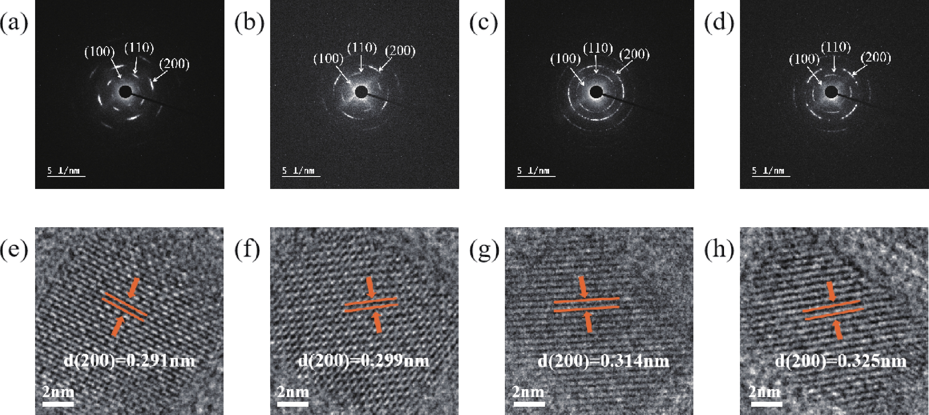
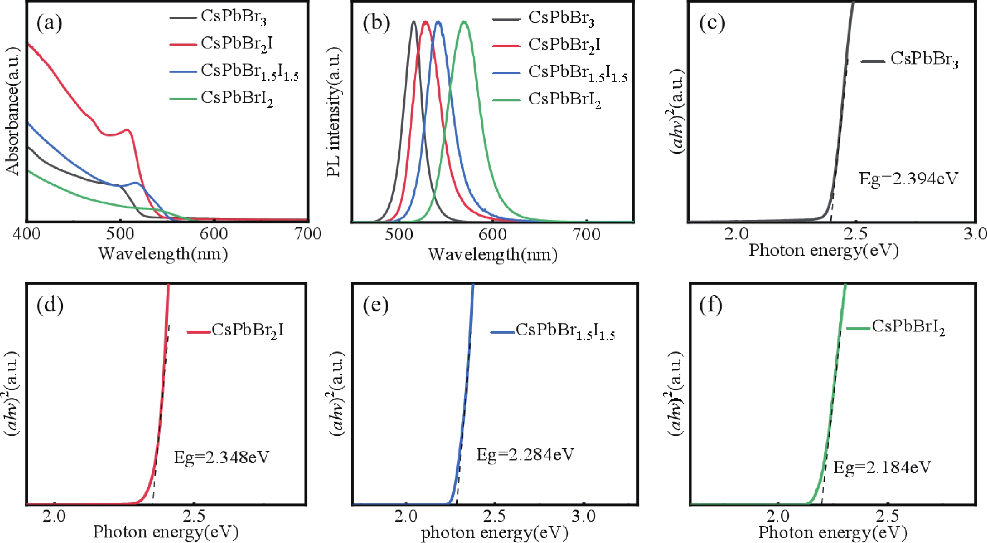
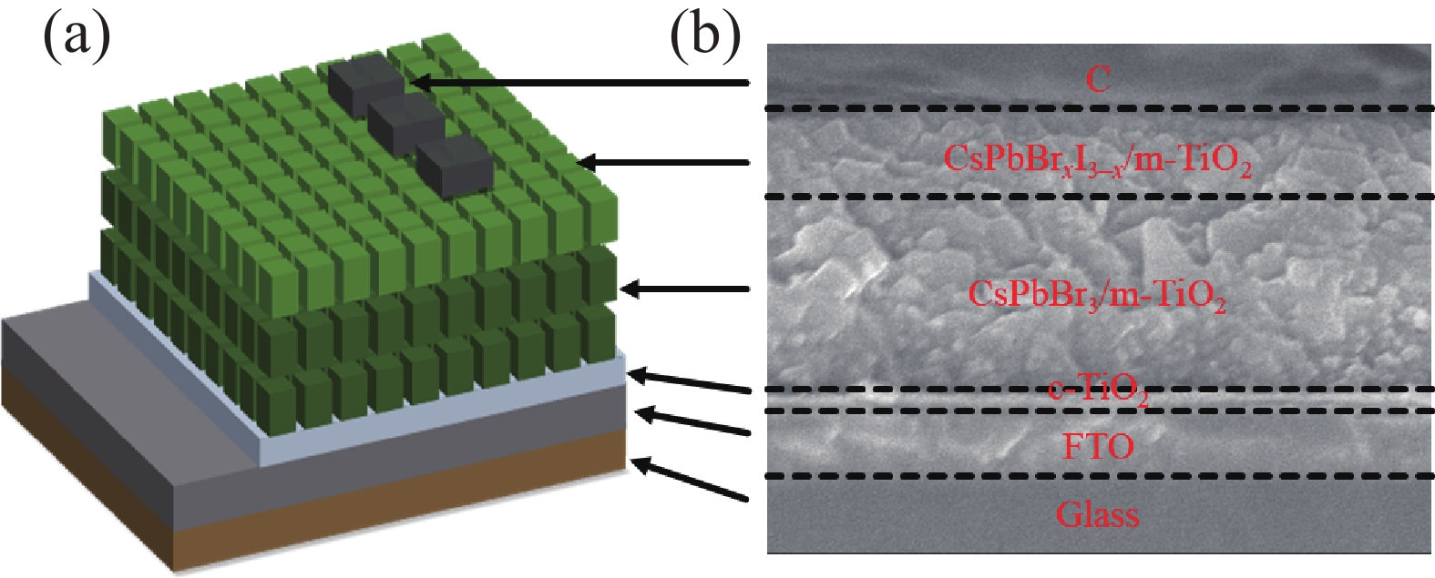
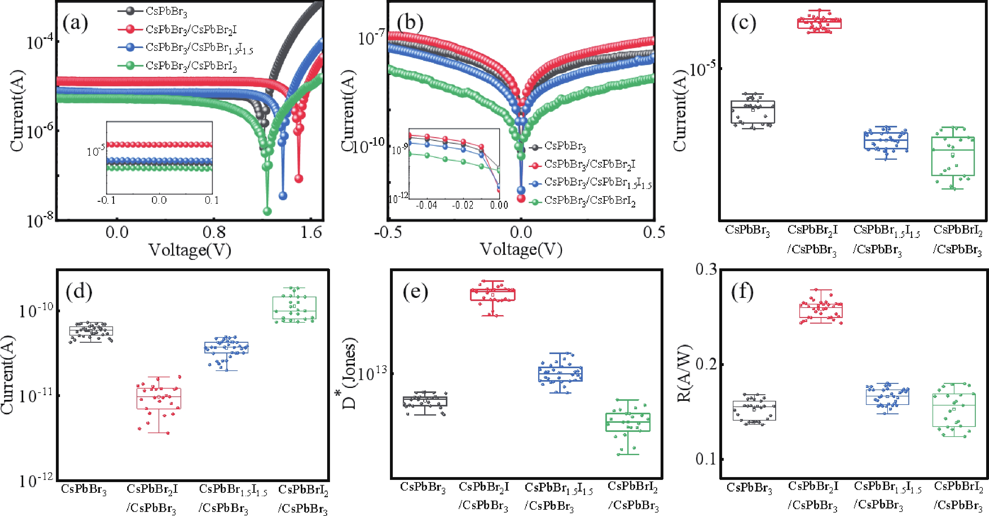
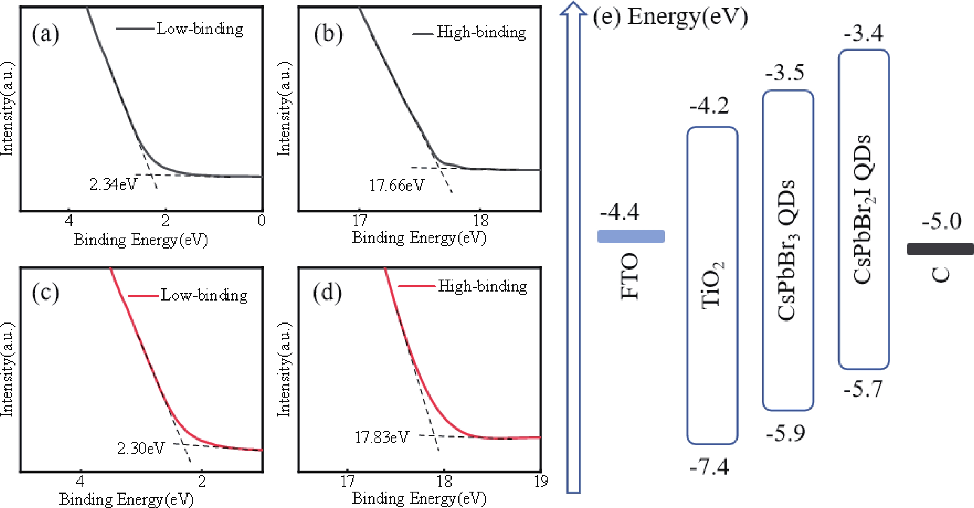
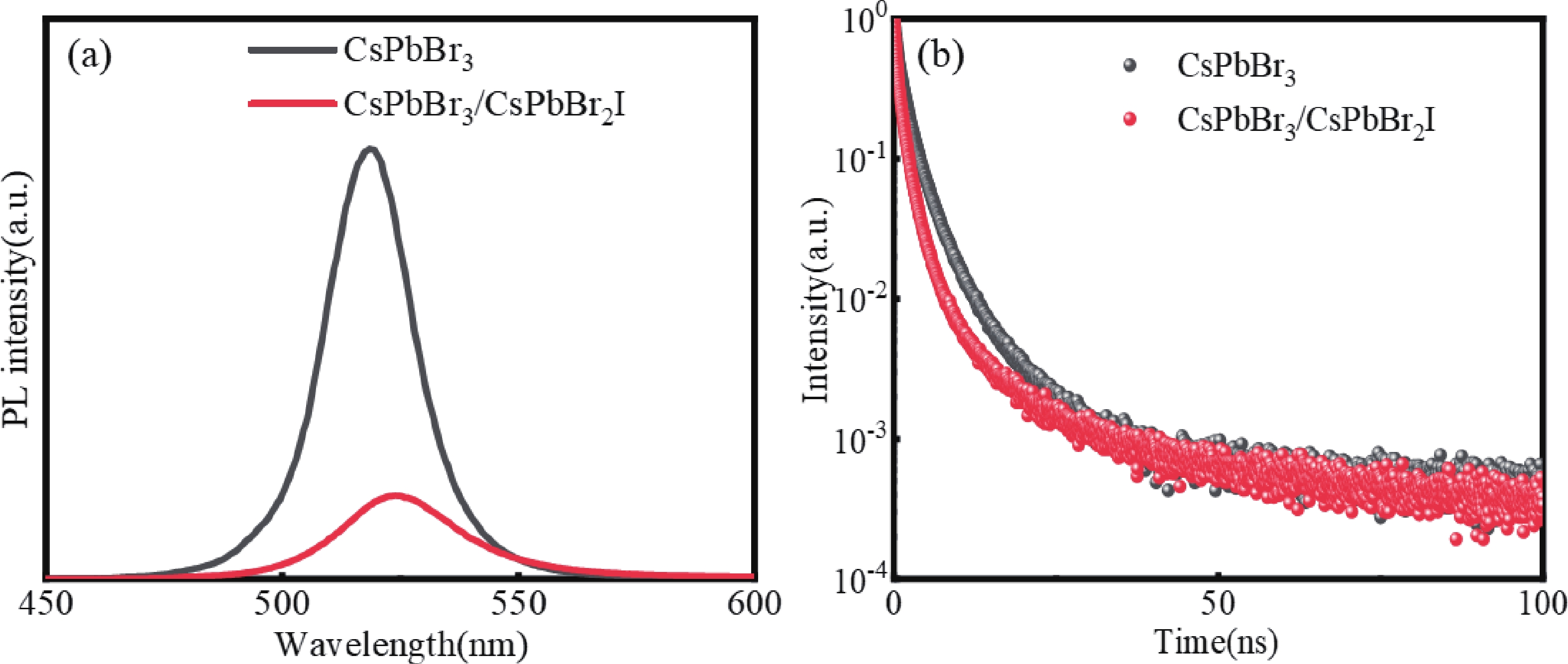
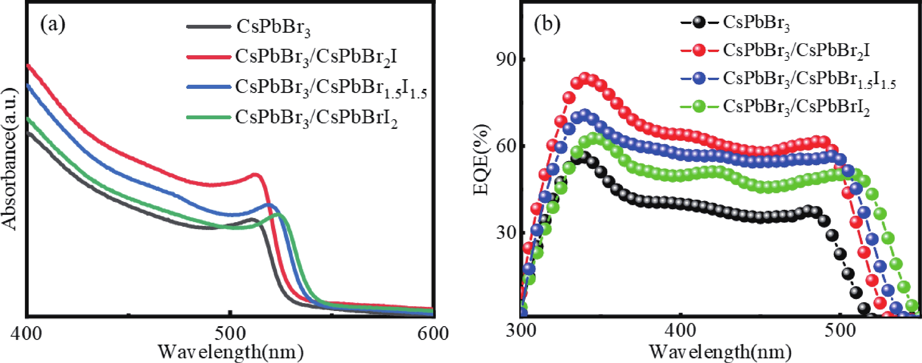
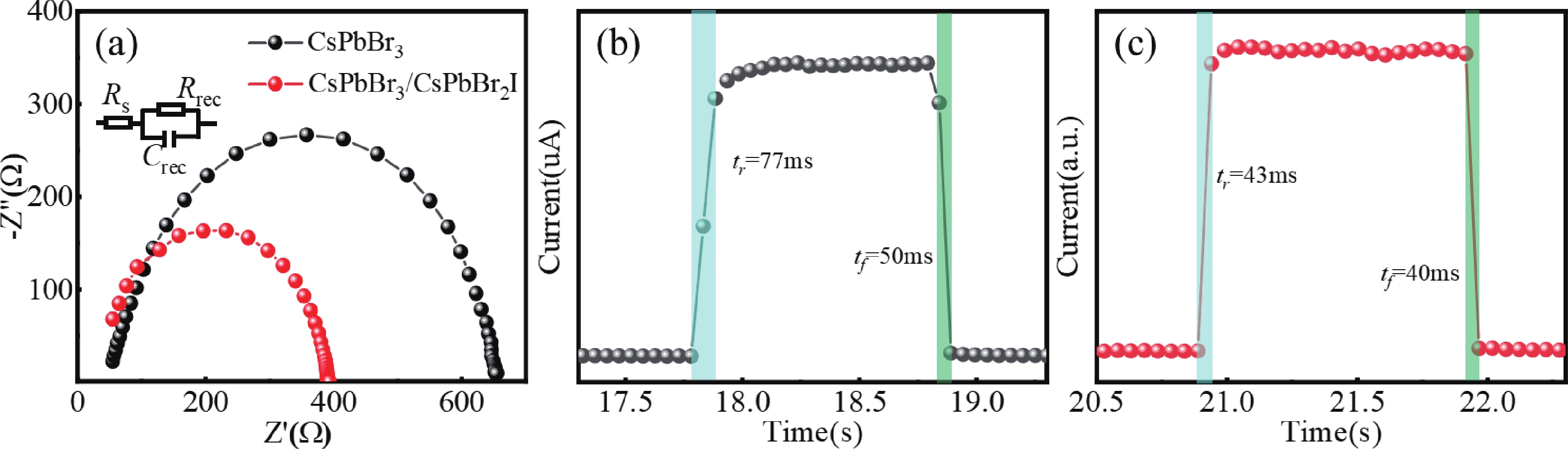
Table 1. Atomic ratio analysis of EDS elements.
| Material | Cs atomic ratio (%) | Pb atomic ratio (%) | Br atomic ratio (%) | I atomic ratio (%) |
| CsPbBr3 | 20.34 | 20.63 | 59.04 | 0 |
| CsPbBr2I | 20.98 | 20.65 | 38.5 | 19.87 |
| CsPbBr1.5I1.5 | 20.42 | 18.90 | 32.14 | 28.54 |
| CsPbBrI2 | 19.39 | 21.07 | 21.7 | 37.84 |
 DownLoad: CSV
Table 2. Interplanar spacing in cubic CsPbBr3 standard PDF card.
| Crystal face | (100) | (110) | (111) | (200) | (210) | (211) | (220) |
| Interplanar distance (Å) | 5.830 | 4.120 | 3.363 | 2.915 | 2.607 | 2.380 | 2.061 |
DownLoad: CSV
Table 3. Interplanar spacing of CsPbBrxI3–x (x = 3, 2, 1.5, 1) QDs diffraction rings.
| Quantum dots |
Diffraction ring diameter (nm–1) |
Interplanar distance (nm) |
| CsPbBr3 | 4.951 | 0.403 |
| 6.99 | 0.291 | |
| CsPbBr2I | 4.924 | 0.409 |
| 6.93 | 0.299 | |
| CsPbBr1.5I1.5 | 4.855 | 0.413 |
| 6.888 | 0.314 | |
| CsPbBrI2 | 4.784 | 0.421 |
| 6.788 | 0.325 |
DownLoad: CSV
Table 4. PL peak positions corresponding to CsPbBrxI3–x (x = 3, 2, 1.5, 1) QDs.
| Description of sample | CsPbBr3 | CsPbBr2I | CsPbBr1.5I1.5 | CsPbBrI2 |
| Peak position (nm) | 515.5 | 528 | 542 | 568.5 |
| Bandgap width (eV) | 2.394 | 2.348 | 2.284 | 2.184 |
DownLoad: CSV
Table 5. TRPL parameters of CsPbBr3 QDs and CsPbBr3 QDs/CsPbBr2I QDs films.
| QDs | t1(ns) | Fraction (A1) |
t2(ns) | Fraction (A2) |
Tave(ns) |
| CsPbBr3 | 0.71 | 0.61 | 2.94 | 0.40 | 2.34 |
| CsPbBr3/CsPbBr2I | 0.47 | 0.68 | 1.95 | 0.32 | 1.45 |
DownLoad: CSV
| [1] |
Yadav S N S, Hanmandlu C, Patel D K, et al. Enhanced photoresponsivity of perovskite QDs/graphene hybrid gate-free photodetector by morphologically controlled plasmonic Au nanocrystals. Adv Opt Mater, 2023, 11(15), 2300131 doi: 10.1002/adom.202300131
|
| [2] |
Liu D, Yin Y X, Liu F J, et al. Thickness-dependent highly sensitive photodetection behavior of lead-free all-inorganic CsSnBr3 nanoplates. Rare Met, 2022, 41(5), 1753 doi: 10.1007/s12598-021-01909-8
|
| [3] |
Mandal A, Ghosh A, Ghosh D, et al. Photodetectors with high responsivity by thickness tunable mixed halide perovskite nanosheets. ACS Appl Mater Interfaces, 2021, 13(36), 43104 doi: 10.1021/acsami.1c13452
|
| [4] |
Chen K Q, Jin W, Zhang Y P, et al. High efficiency mesoscopic solar cells using CsPbI3 perovskite quantum dots enabled by chemical interface engineering. J Am Chem Soc, 2020, 142(8), 3775 doi: 10.1021/jacs.9b10700
|
| [5] |
Han M M, Sun J M, Peng M, et al. Controllable growth of lead-free all-inorganic perovskite nanowire array with fast and stable near-infrared photodetection. J Phys Chem C, 2019, 123(28), 17566 doi: 10.1021/acs.jpcc.9b03289
|
| [6] |
Jing H, Peng R W, Ma R M, et al. Flexible ultrathin single-crystalline perovskite photodetector. Nano Lett, 2020, 20(10), 7144 doi: 10.1021/acs.nanolett.0c02468
|
| [7] |
Popoola A, Gondal M A, Popoola I K, et al. Fabrication of bifacial sandwiched heterojunction photoconductor–Type and MAI passivated photodiode–Type perovskite photodetectors. Org Electron, 2020, 84, 105730 doi: 10.1016/j.orgel.2020.105730
|
| [8] |
Jia D L, Chen J X, Zhuang R S, et al. Antisolvent-assisted in situ cation exchange of perovskite quantum dots for efficient solar cells. Adv Mater, 2023, 35(21), e2212160 doi: 10.1002/adma.202212160
|
| [9] |
Yang Z, Xu Q, Wang X D, et al. Large and ultrastable all-inorganic CsPbBr3 monocrystalline films: Low-temperature growth and application for high-performance photodetectors. Adv Mater, 2018, 30(44), e1802110 doi: 10.1002/adma.201802110
|
| [10] |
Li J, Zhang G D, Zhang Z H, et al. Defect passivation via additive engineering to improve photodetection performance in CsPbI2Br perovskite photodetectors. ACS Appl Mater Interfaces, 2021, 13(47), 56358 doi: 10.1021/acsami.1c19323
|
| [11] |
Liu S L, Gao W Q, Chen Y, et al. Van der waals integration of large-area monocrystalline 3D perovskite thin films on arbitrary semiconductor substrates for heterojunctions. Nano Lett, 2024, 24(25), 7724 doi: 10.1021/acs.nanolett.4c01715
|
| [12] |
Zhu H W, Tong G Q, Li J C, et al. Enriched-bromine surface state for stable sky-blue spectrum perovskite QLEDs with an EQE of 14.6. Adv Mater, 2022, 34(37), e2205092 doi: 10.1002/adma.202205092
|
| [13] |
Li S, Shi Z F, Zhang F, et al. Sodium doping-enhanced emission efficiency and stability of CsPbBr3 nanocrystals for white light-emitting devices. Chem Mater, 2019, 31(11), 3917 doi: 10.1021/acs.chemmater.8b05362
|
| [14] |
Chen H J, Zhang M, Fu X, et al. Light-activated inorganic CsPbBr2I perovskite for room-temperature self-powered chemical sensing. Phys Chem Chem Phys, 2019, 21(43), 24187 doi: 10.1039/C9CP03059J
|
| [15] |
Chen Y L, Hu Y H, Ma L, et al. Self-assembled CsPbBr3 quantum dots with wavelength-tunable photoluminescence for efficient active jamming. Nanoscale, 2022, 14(48), 17900 doi: 10.1039/D2NR05314D
|
| [16] |
Shen K, Xu H, Li X, et al. Flexible and self-powered photodetector arrays based on all-inorganic CsPbBr3 quantum dots. Adv Mater, 2020, 32(22), e2000004 doi: 10.1002/adma.202000004
|
| [17] |
Cong H, Chu X B, Wan F S, et al. Broadband photodetector based on inorganic perovskite CsPbBr3/GeSn heterojunction. Small Methods, 2021, 5(8), e2100517 doi: 10.1002/smtd.202100517
|
| [18] |
Liu Q B, Liang L H, Shen H Z, et al. Epitaxial growth of CsPbBr3-PbS vertical and lateral heterostructures for visible to infrared broadband photodetection. Nano Res, 2021, 14(11), 3879 doi: 10.1007/s12274-021-3308-0
|
| [19] |
Han Y, Li G H, Ji T, et al. Detecting visible to near-infrared II light via CsPbBr3 nanocrystals/Y6 heterojunctions. ACS Appl Mater Interfaces, 2024, 16(19), 25385 doi: 10.1021/acsami.4c03712
|
| [20] |
Kim M, Bae G, Kim K N, et al. Perovskite quantum dot-induced monochromatization for broadband photodetection of wafer-scale molybdenum disulfide. NPG Asia Mater, 2022, 14, 89 doi: 10.1038/s41427-022-00435-y
|
| [21] |
Jeong S J, Cho S, Moon B, et al. Zero dimensional-two dimensional hybrid photodetectors using multilayer MoS2 and lead halide perovskite quantum dots with a tunable bandgap. ACS Appl Mater Interfaces, 2023, 15(4), 5432 doi: 10.1021/acsami.2c17200
|
| [22] |
Li Z B, Li H N, Jiang K, et al. Self-powered perovskite/CdS heterostructure photodetectors. ACS Appl Mater Interfaces, 2019, 11(43), 40204 doi: 10.1021/acsami.9b11835
|
| [23] |
Ding N, Wu Y J, Xu W, et al. A novel approach for designing efficient broadband photodetectors expanding from deep ultraviolet to near infrared. Light Sci Appl, 2022, 11(1), 91 doi: 10.1038/s41377-022-00777-w
|
| [24] |
Li Z B, Li J N, Ding D, et al. Direct observation of perovskite photodetector performance enhancement by atomically thin interface engineering. ACS Appl Mater Interfaces, 2018, 10(42), 36493 doi: 10.1021/acsami.8b10971
|
| [25] |
Min X, Jiang F Y, Qin F, et al. Polyethylenimine aqueous solution: A low-cost and environmentally friendly formulation to produce low-work-function electrodes for efficient easy-to-fabricate organic solar cells. ACS Appl Mater Interfaces, 2014, 6(24), 22628 doi: 10.1021/am5077974
|
| [26] |
Imran M, Peng L C, Pianetti A, et al. Halide perovskite-lead chalcohalide nanocrystal heterostructures. J Am Chem Soc, 2021, 143(3), 1435 doi: 10.1021/jacs.0c10916
|
| [27] |
Yao E P, Bohn B J, Tong Y, et al. Exciton diffusion lengths and dissociation rates in CsPbBr3 nanocrystal–fullerene composites: Layer-by-layer versus blend structures. Adv Opt Mater, 2019, 7(8), 1801776 doi: 10.1002/adom.201801776
|
| [28] |
Guan Y W, Zhang C H, Liu Z, et al. Single-crystalline perovskite p-n junction nanowire arrays for ultrasensitive photodetection. Adv Mater, 2022, 34(35), e2203201 doi: 10.1002/adma.202203201
|
| [29] |
Liu S L, Chen Y, Gao W Q, et al. Epitaxy of a monocrystalline CsPbBr3-SrTiO3 halide-oxide perovskite p-n heterojunction with high stability for photodetection. Adv Mater, 2023, 35(31), e2303544 doi: 10.1002/adma.202303544
|
| [30] |
Zhang T. Study on the preparation of lead-based perovskite thin films and application of optoelectronic devices. University of Electronic Science and Technology of China, 2020
|
| [31] |
Zhang Z, Zhang W T, Jiang Q B, et al. Toward high-performance electron/hole-transporting-layer-free, self-powered CsPbIBr2 photodetectors via interfacial engineering. ACS Appl Mater Interfaces, 2020, 12(5), 6607 doi: 10.1021/acsami.9b19075
|
| [32] |
Wieliczka B M, Habisreutinger S N, Schutt K, et al. Nanocrystal-enabled perovskite heterojunctions in photovoltaic applications and beyond. Adv Energy Mater, 2023, 13(22), 2204351 doi: 10.1002/aenm.202204351
|
| [33] |
Deng J D, Wang H R, Xun J, et al. Room-temperature synthesis of excellent-performance CsPb1–xSnxBr3 perovskite quantum dots and application in light emitting diodes. Mater Des, 2020, 185, 108246 doi: 10.1016/j.matdes.2019.108246
|
| [34] |
Jing Q, Zhang M, Huang X, et al. Surface passivation of mixed-halide perovskite CsPb(BrxI1–x)3 nanocrystals by selective etching for improved stability. Nanoscale, 2017, 9(22), 7391 doi: 10.1039/C7NR01287J
|
| [35] |
Nedelcu G, Protesescu L, Yakunin S, et al. Fast anion-exchange in highly luminescent nanocrystals of cesium lead halide perovskites (CsPbX3, X = Cl, Br, I). Nano Lett, 2015, 15(8), 5635 doi: 10.1021/acs.nanolett.5b02404
|
| [36] |
Hautzinger M P, Raulerson E K, Harvey S P, et al. Metal halide perovskite heterostructures: Blocking anion diffusion with single-layer graphene. J Am Chem Soc, 2023, 145(4), 2052 doi: 10.1021/jacs.2c12441
|


Article views: 1235 Times PDF downloads: 108 Times Cited by: 0 Times
Received: 16 January 2025 Revised: 25 March 2025 Online: Accepted Manuscript: 14 April 2025Uncorrected proof: 19 May 2025Published: 09 October 2025
| Citation: |
Chenguang Shen, Mengwei Chen, Wei Huang, Yingping Yang. Research on heterojunction semiconductor photodetectors based on CsPbBr3 QDs/CsPbBrxI3–x QDs[J]. Journal of Semiconductors, 2025, 46(10): 102801. doi: 10.1088/1674-4926/25010022
****
C G Shen, M W Chen, W Huang, and Y P Yang, Research on heterojunction semiconductor photodetectors based on CsPbBr3 QDs/CsPbBrxI3–x QDs[J]. J. Semicond., 2025, 46(10), 102801 doi: 10.1088/1674-4926/25010022

|
 Chenguang Shen is a postgraduate student in the School of Physics and Mechanics of Wuhan University of Technology. Her tutors are Associate Professor Mengwei Chen and Professor Yingping Yang. The main research direction is quantum dot photodetectors
 Mengwei Chen is a Associate Professor in the Department of Physics at Wuhan University of Technology. Her research direction is optoelectronic materials and devices
 Yingping Yang is a professor in the Department of Physics at Wuhan University of Technology, specializing in the research of optoelectronic materials and device physics
| [1] |
Yadav S N S, Hanmandlu C, Patel D K, et al. Enhanced photoresponsivity of perovskite QDs/graphene hybrid gate-free photodetector by morphologically controlled plasmonic Au nanocrystals. Adv Opt Mater, 2023, 11(15), 2300131 doi: 10.1002/adom.202300131
|
| [2] |
Liu D, Yin Y X, Liu F J, et al. Thickness-dependent highly sensitive photodetection behavior of lead-free all-inorganic CsSnBr3 nanoplates. Rare Met, 2022, 41(5), 1753 doi: 10.1007/s12598-021-01909-8
|
| [3] |
Mandal A, Ghosh A, Ghosh D, et al. Photodetectors with high responsivity by thickness tunable mixed halide perovskite nanosheets. ACS Appl Mater Interfaces, 2021, 13(36), 43104 doi: 10.1021/acsami.1c13452
|
| [4] |
Chen K Q, Jin W, Zhang Y P, et al. High efficiency mesoscopic solar cells using CsPbI3 perovskite quantum dots enabled by chemical interface engineering. J Am Chem Soc, 2020, 142(8), 3775 doi: 10.1021/jacs.9b10700
|
| [5] |
Han M M, Sun J M, Peng M, et al. Controllable growth of lead-free all-inorganic perovskite nanowire array with fast and stable near-infrared photodetection. J Phys Chem C, 2019, 123(28), 17566 doi: 10.1021/acs.jpcc.9b03289
|
| [6] |
Jing H, Peng R W, Ma R M, et al. Flexible ultrathin single-crystalline perovskite photodetector. Nano Lett, 2020, 20(10), 7144 doi: 10.1021/acs.nanolett.0c02468
|
| [7] |
Popoola A, Gondal M A, Popoola I K, et al. Fabrication of bifacial sandwiched heterojunction photoconductor–Type and MAI passivated photodiode–Type perovskite photodetectors. Org Electron, 2020, 84, 105730 doi: 10.1016/j.orgel.2020.105730
|
| [8] |
Jia D L, Chen J X, Zhuang R S, et al. Antisolvent-assisted in situ cation exchange of perovskite quantum dots for efficient solar cells. Adv Mater, 2023, 35(21), e2212160 doi: 10.1002/adma.202212160
|
| [9] |
Yang Z, Xu Q, Wang X D, et al. Large and ultrastable all-inorganic CsPbBr3 monocrystalline films: Low-temperature growth and application for high-performance photodetectors. Adv Mater, 2018, 30(44), e1802110 doi: 10.1002/adma.201802110
|
| [10] |
Li J, Zhang G D, Zhang Z H, et al. Defect passivation via additive engineering to improve photodetection performance in CsPbI2Br perovskite photodetectors. ACS Appl Mater Interfaces, 2021, 13(47), 56358 doi: 10.1021/acsami.1c19323
|
| [11] |
Liu S L, Gao W Q, Chen Y, et al. Van der waals integration of large-area monocrystalline 3D perovskite thin films on arbitrary semiconductor substrates for heterojunctions. Nano Lett, 2024, 24(25), 7724 doi: 10.1021/acs.nanolett.4c01715
|
| [12] |
Zhu H W, Tong G Q, Li J C, et al. Enriched-bromine surface state for stable sky-blue spectrum perovskite QLEDs with an EQE of 14.6. Adv Mater, 2022, 34(37), e2205092 doi: 10.1002/adma.202205092
|
| [13] |
Li S, Shi Z F, Zhang F, et al. Sodium doping-enhanced emission efficiency and stability of CsPbBr3 nanocrystals for white light-emitting devices. Chem Mater, 2019, 31(11), 3917 doi: 10.1021/acs.chemmater.8b05362
|
| [14] |
Chen H J, Zhang M, Fu X, et al. Light-activated inorganic CsPbBr2I perovskite for room-temperature self-powered chemical sensing. Phys Chem Chem Phys, 2019, 21(43), 24187 doi: 10.1039/C9CP03059J
|
| [15] |
Chen Y L, Hu Y H, Ma L, et al. Self-assembled CsPbBr3 quantum dots with wavelength-tunable photoluminescence for efficient active jamming. Nanoscale, 2022, 14(48), 17900 doi: 10.1039/D2NR05314D
|
| [16] |
Shen K, Xu H, Li X, et al. Flexible and self-powered photodetector arrays based on all-inorganic CsPbBr3 quantum dots. Adv Mater, 2020, 32(22), e2000004 doi: 10.1002/adma.202000004
|
| [17] |
Cong H, Chu X B, Wan F S, et al. Broadband photodetector based on inorganic perovskite CsPbBr3/GeSn heterojunction. Small Methods, 2021, 5(8), e2100517 doi: 10.1002/smtd.202100517
|
| [18] |
Liu Q B, Liang L H, Shen H Z, et al. Epitaxial growth of CsPbBr3-PbS vertical and lateral heterostructures for visible to infrared broadband photodetection. Nano Res, 2021, 14(11), 3879 doi: 10.1007/s12274-021-3308-0
|
| [19] |
Han Y, Li G H, Ji T, et al. Detecting visible to near-infrared II light via CsPbBr3 nanocrystals/Y6 heterojunctions. ACS Appl Mater Interfaces, 2024, 16(19), 25385 doi: 10.1021/acsami.4c03712
|
| [20] |
Kim M, Bae G, Kim K N, et al. Perovskite quantum dot-induced monochromatization for broadband photodetection of wafer-scale molybdenum disulfide. NPG Asia Mater, 2022, 14, 89 doi: 10.1038/s41427-022-00435-y
|
| [21] |
Jeong S J, Cho S, Moon B, et al. Zero dimensional-two dimensional hybrid photodetectors using multilayer MoS2 and lead halide perovskite quantum dots with a tunable bandgap. ACS Appl Mater Interfaces, 2023, 15(4), 5432 doi: 10.1021/acsami.2c17200
|
| [22] |
Li Z B, Li H N, Jiang K, et al. Self-powered perovskite/CdS heterostructure photodetectors. ACS Appl Mater Interfaces, 2019, 11(43), 40204 doi: 10.1021/acsami.9b11835
|
| [23] |
Ding N, Wu Y J, Xu W, et al. A novel approach for designing efficient broadband photodetectors expanding from deep ultraviolet to near infrared. Light Sci Appl, 2022, 11(1), 91 doi: 10.1038/s41377-022-00777-w
|
| [24] |
Li Z B, Li J N, Ding D, et al. Direct observation of perovskite photodetector performance enhancement by atomically thin interface engineering. ACS Appl Mater Interfaces, 2018, 10(42), 36493 doi: 10.1021/acsami.8b10971
|
| [25] |
Min X, Jiang F Y, Qin F, et al. Polyethylenimine aqueous solution: A low-cost and environmentally friendly formulation to produce low-work-function electrodes for efficient easy-to-fabricate organic solar cells. ACS Appl Mater Interfaces, 2014, 6(24), 22628 doi: 10.1021/am5077974
|
| [26] |
Imran M, Peng L C, Pianetti A, et al. Halide perovskite-lead chalcohalide nanocrystal heterostructures. J Am Chem Soc, 2021, 143(3), 1435 doi: 10.1021/jacs.0c10916
|
| [27] |
Yao E P, Bohn B J, Tong Y, et al. Exciton diffusion lengths and dissociation rates in CsPbBr3 nanocrystal–fullerene composites: Layer-by-layer versus blend structures. Adv Opt Mater, 2019, 7(8), 1801776 doi: 10.1002/adom.201801776
|
| [28] |
Guan Y W, Zhang C H, Liu Z, et al. Single-crystalline perovskite p-n junction nanowire arrays for ultrasensitive photodetection. Adv Mater, 2022, 34(35), e2203201 doi: 10.1002/adma.202203201
|
| [29] |
Liu S L, Chen Y, Gao W Q, et al. Epitaxy of a monocrystalline CsPbBr3-SrTiO3 halide-oxide perovskite p-n heterojunction with high stability for photodetection. Adv Mater, 2023, 35(31), e2303544 doi: 10.1002/adma.202303544
|
| [30] |
Zhang T. Study on the preparation of lead-based perovskite thin films and application of optoelectronic devices. University of Electronic Science and Technology of China, 2020
|
| [31] |
Zhang Z, Zhang W T, Jiang Q B, et al. Toward high-performance electron/hole-transporting-layer-free, self-powered CsPbIBr2 photodetectors via interfacial engineering. ACS Appl Mater Interfaces, 2020, 12(5), 6607 doi: 10.1021/acsami.9b19075
|
| [32] |
Wieliczka B M, Habisreutinger S N, Schutt K, et al. Nanocrystal-enabled perovskite heterojunctions in photovoltaic applications and beyond. Adv Energy Mater, 2023, 13(22), 2204351 doi: 10.1002/aenm.202204351
|
| [33] |
Deng J D, Wang H R, Xun J, et al. Room-temperature synthesis of excellent-performance CsPb1–xSnxBr3 perovskite quantum dots and application in light emitting diodes. Mater Des, 2020, 185, 108246 doi: 10.1016/j.matdes.2019.108246
|
| [34] |
Jing Q, Zhang M, Huang X, et al. Surface passivation of mixed-halide perovskite CsPb(BrxI1–x)3 nanocrystals by selective etching for improved stability. Nanoscale, 2017, 9(22), 7391 doi: 10.1039/C7NR01287J
|
| [35] |
Nedelcu G, Protesescu L, Yakunin S, et al. Fast anion-exchange in highly luminescent nanocrystals of cesium lead halide perovskites (CsPbX3, X = Cl, Br, I). Nano Lett, 2015, 15(8), 5635 doi: 10.1021/acs.nanolett.5b02404
|
| [36] |
Hautzinger M P, Raulerson E K, Harvey S P, et al. Metal halide perovskite heterostructures: Blocking anion diffusion with single-layer graphene. J Am Chem Soc, 2023, 145(4), 2052 doi: 10.1021/jacs.2c12441
|

 WeChat ID
Journal of Semiconductors © 2017 All Rights Reserved 京ICP备05085259号-2


