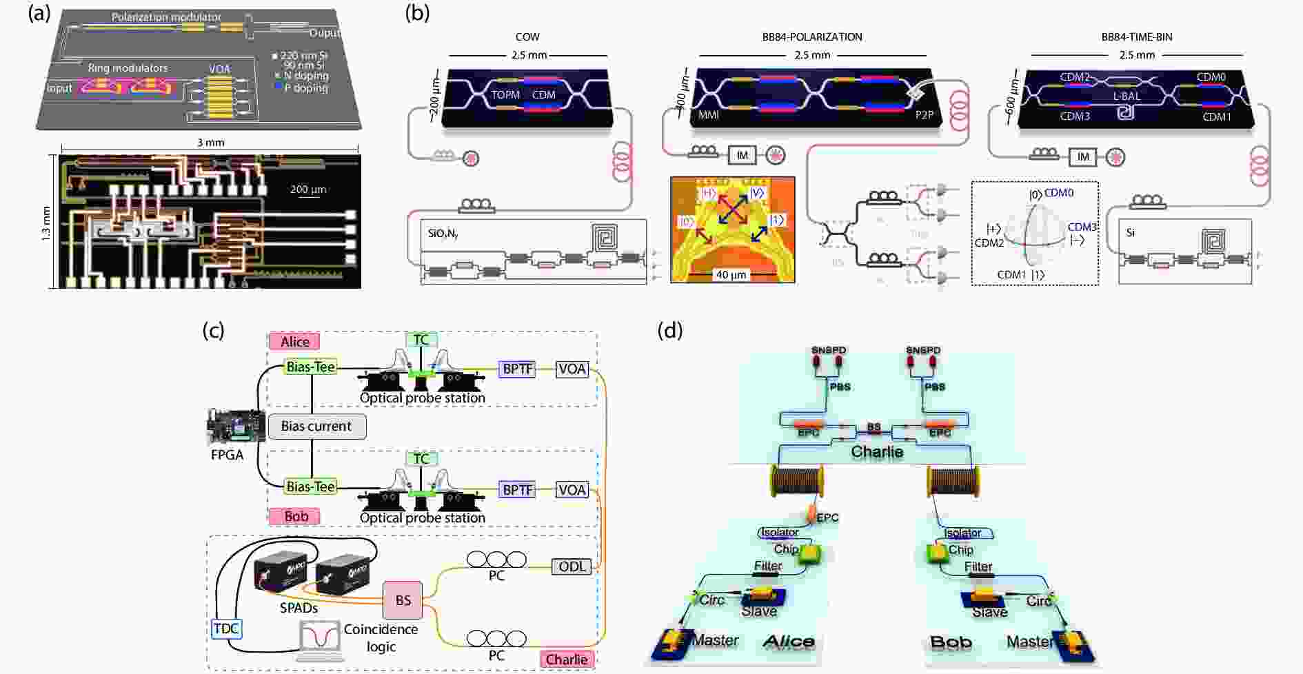
Quantum communications aim to share encryption keys between the transmitters and receivers governed by the laws of quantum mechanics. Integrated quantum photonics offers significant advantages of dense integration, high stability and scalability, which enables a vital platform for the implementation of quantum information processing and quantum communications. This article reviews recent experimental progress and advances in the development of integrated quantum photonic devices and systems for quantum communications and quantum networks.

Two-dimensional/one-dimensional (2D/1D) heterostructures as a new type of heterostructure have been studied for their unusual properties and promising applications in electronic and optoelectronic devices. However, the studies of 2D/1D heterostructures are mainly focused on vertical heterostructures, such as MoS2 nanosheet-carbon nanotubes. The research on lateral 2D/1D heterostructures with a tunable width of 1D material is still scarce. In this study, bidirectional flow chemical vapor deposition (CVD) was used to accurately control the width of the WS2/WSe2 (WS2/MoS2) heterostructures by controlling reacting time. WSe2 and MoS2 with different widths were epitaxially grown at the edge of WS2, respectively. Optical microscope, atomic force microscope (AFM), and scanning electron microscope (SEM) images show the morphology and width of the heterostructures. These results show that the width of the heterostructures can be as low as 10 nm by using this method. The interface of the heterostructure is clear and smooth, which is suitable for application. This report offers a new method for the growth of 1D nanowires, and lays the foundation for the future study of the physical and chemical properties of 2D/1D lateral heterostructures.

The ultrahigh vacuum scanning tunneling microscope (STM) was used to characterize the GaSb1–xBix films of a few nanometers thickness grown by the molecular beam epitaxy (MBE) on the GaSb buffer layer of 100 nm with the GaSb (100) substrates. The thickness of the GaSb1–xBix layers of the samples are 5 and 10 nm, respectively. For comparison, the GaSb buffer was also characterized and its STM image displays terraces whose surfaces are basically atomically flat and their roughness is generally less than 1 monolayer (ML). The surface of 5 nm GaSb1–xBix film reserves the same terraced morphology as the buffer layer. In contrast, the morphology of the 10 nm GaSb1–xBix film changes to the mound-like island structures with a height of a few MLs. The result implies the growth mode transition from the two-dimensional mode as displayed by the 5 nm film to the Stranski–Krastinov mode as displayed by the 10 nm film. The statistical analysis with the scanning tunneling spectroscopy (STS) measurements indicates that both the incorporation and the inhomogeneity of Bi atoms increase with the thickness of the GaSb1–xBix layer.

A 300 kbps wide-angle non-line-of-sight ultraviolet communication system with voice transmission function is designed here. Based on Poisson distribution theory, we design the symbol detecting method for the receiving discrete photon signals. Using 272 nm LED array as the light source and PMT as the detector, the voice transceiver is integrated into the carriable size of 200 × 90 × 65 mm3. An outfield test shows the system obtains the BER of 0.88% under 200 m. Under 10° wide-angle deviation of the transmitter, a BER below 1.33% is achieved.
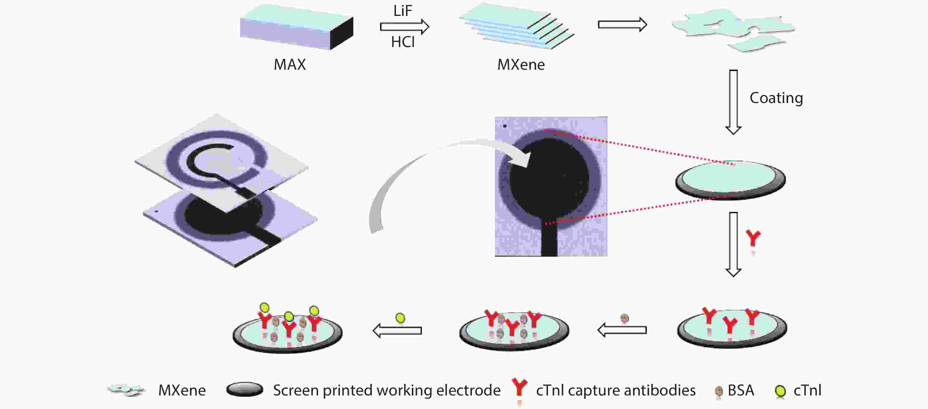
Convenient, rapid, and accurate detection of cardiac troponin I (cTnI) is crucial in early diagnosis of acute myocardial infarction (AMI). A paper-based electrochemical immunosensor is a promising choice in this field, because of the flexibility, porosity, and cost-efficacy of the paper. However, paper is poor in electronic conductivity and surface functionality. Herein, we report a paper-based electrochemical immunosensor for the label-free detection of cTnI with the working electrode modified by MXene (Ti3C2) nanosheets. In order to immobilize the bio-receptor (anti-cTnI) on the MXene-modified working electrode, the MXene nanosheets were functionalized by aminosilane, and the functionalized MXene was immobilized onto the surface of the working electrode through Nafion. The large surface area of the MXene nanosheets facilitates the immobilization of antibodies, and the excellent conductivity facilitates the electron transfer between the electrochemical species and the underlying electrode surface. As a result, the paper-based immunosensor could detect cTnI within a wide range of 5–100 ng/mL with a detection limit of 0.58 ng/mL. The immunosensor also shows outstanding selectivity and good repeatability. Our MXene-modified paper-based electrochemical immunosensor enables fast and sensitive detection of cTnI, which may be used in real-time and cost-efficient monitoring of AMI diseases in clinics.

A pre-ohmic micro-patterned recess process, is utilized to fabricate Ti/Al/Ti/TiN ohmic contact to an ultrathin-barrier (UTB) AlGaN/GaN heterostructure, featuring a significantly reduced ohmic contact resistivity of 0.56 Ω·mm at an alloy temperature of 550 °C. The sheet resistances increase with the temperature following a power law with the index of +2.58, while the specific contact resistivity decreases with the temperature. The contact mechanism can be well described by thermionic field emission (TFE). The extracted Schottky barrier height and electron concentration are 0.31 eV and 5.52 × 1018 cm−3, which suggests an intimate contact between ohmic metal and the UTB-AlGaN as well as GaN buffer. A good correlation between ohmic transfer length and the micro-pattern size is revealed, though in-depth investigation is needed. A preliminary CMOS-process-compatible metal–insulator–semiconductor high-mobility transistor (MIS-HEMT) was fabricated with the proposed Au-free ohmic contact technique.
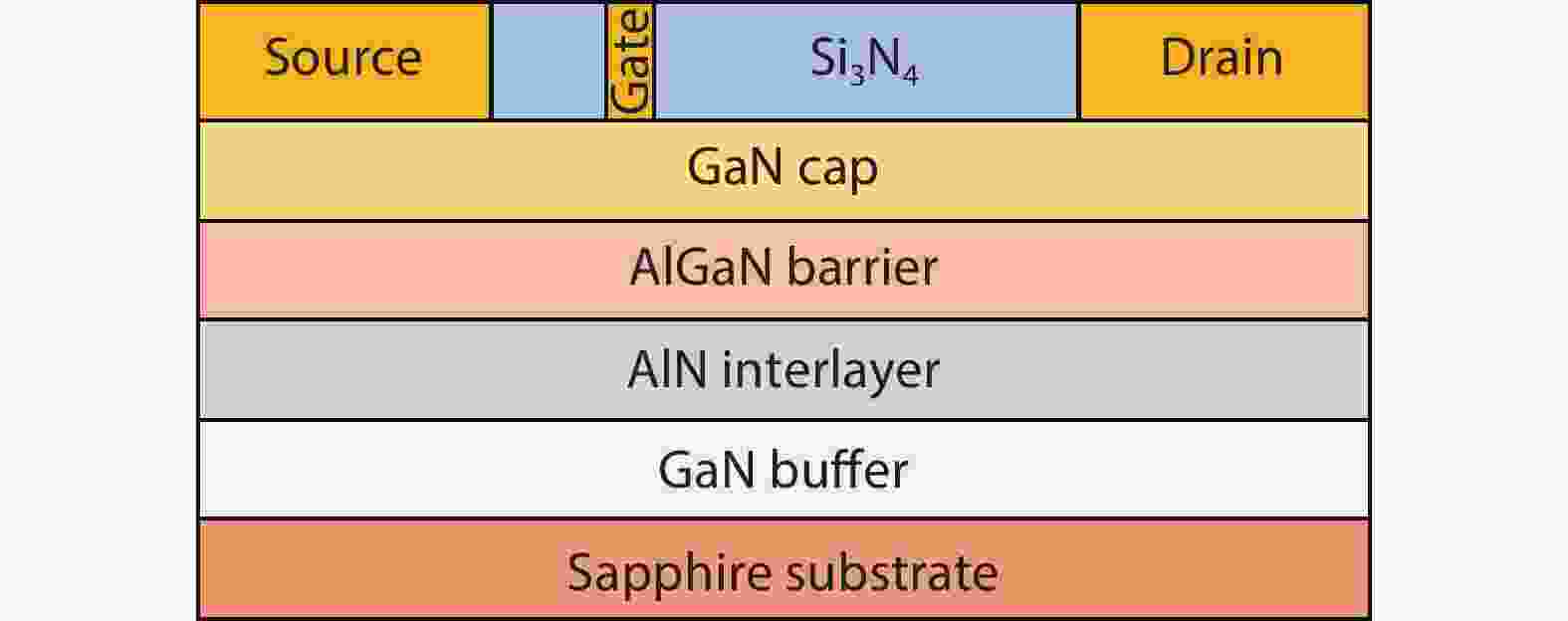
In this paper, we investigated the effect of post-gate annealing (PGA) on reverse gate leakage and the reverse bias reliability of Al0.23Ga0.77N/GaN high electron mobility transistors (HEMTs). We found that the Poole–Frenkel (PF) emission is dominant in the reverse gate leakage current at the low reverse bias region (Vth < VG < 0 V) for the unannealed and annealed HEMTs. The emission barrier height of HEMT is increased from 0.139 to 0.256 eV after the PGA process, which results in a reduction of the reverse leakage current by more than one order. Besides, the reverse step stress was conducted to study the gate reliability of both HEMTs. After the stress, the unannealed HEMT shows a higher reverse leakage current due to the permanent damage of the Schottky gate. In contrast, the annealed HEMT shows a little change in reverse leakage current. This indicates that the PGA can reduce the reverse gate leakage and improve the gate reliability.
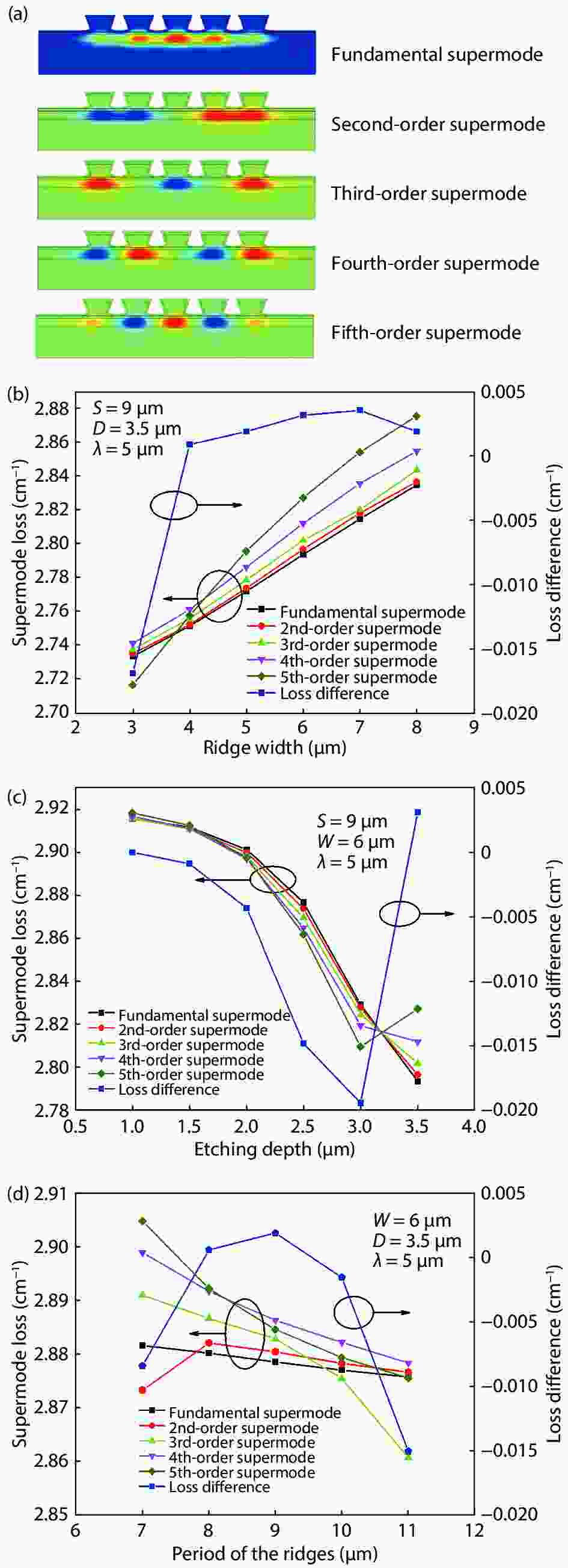
In this work, we demonstrated high-power quantum cascade laser (QCL) arrays lasing at λ ~ 5 µm by employing an optimized coupled-ridge waveguide (CRW) structure. Five-element QCL arrays were simulated and fabricated through a two-step etching method to extend the CRW structure to a mid-wave infrared regime. A lateral far-field with the main peak near a diffraction-limited intensity curve of about 10° was observed by properly designing a geometric shape of the ridges and interspaces. By introducing a buried 2nd-order distributed feedback (DFB) grating, substrate emission with a radiation power above 1 W at 25 °C is achieved. Single longitudinal mode operation is obtained by changing the temperature of the heatsink with a good linear wavelength tuning coefficient of –0.2 cm–1/K.


-01.jpg)


