Issue Browser
Volume 46, Issue 5,
May 2025


J. Semicond.
2025, 46(5): 051801 doi: 10.1088/1674-4926/24090031

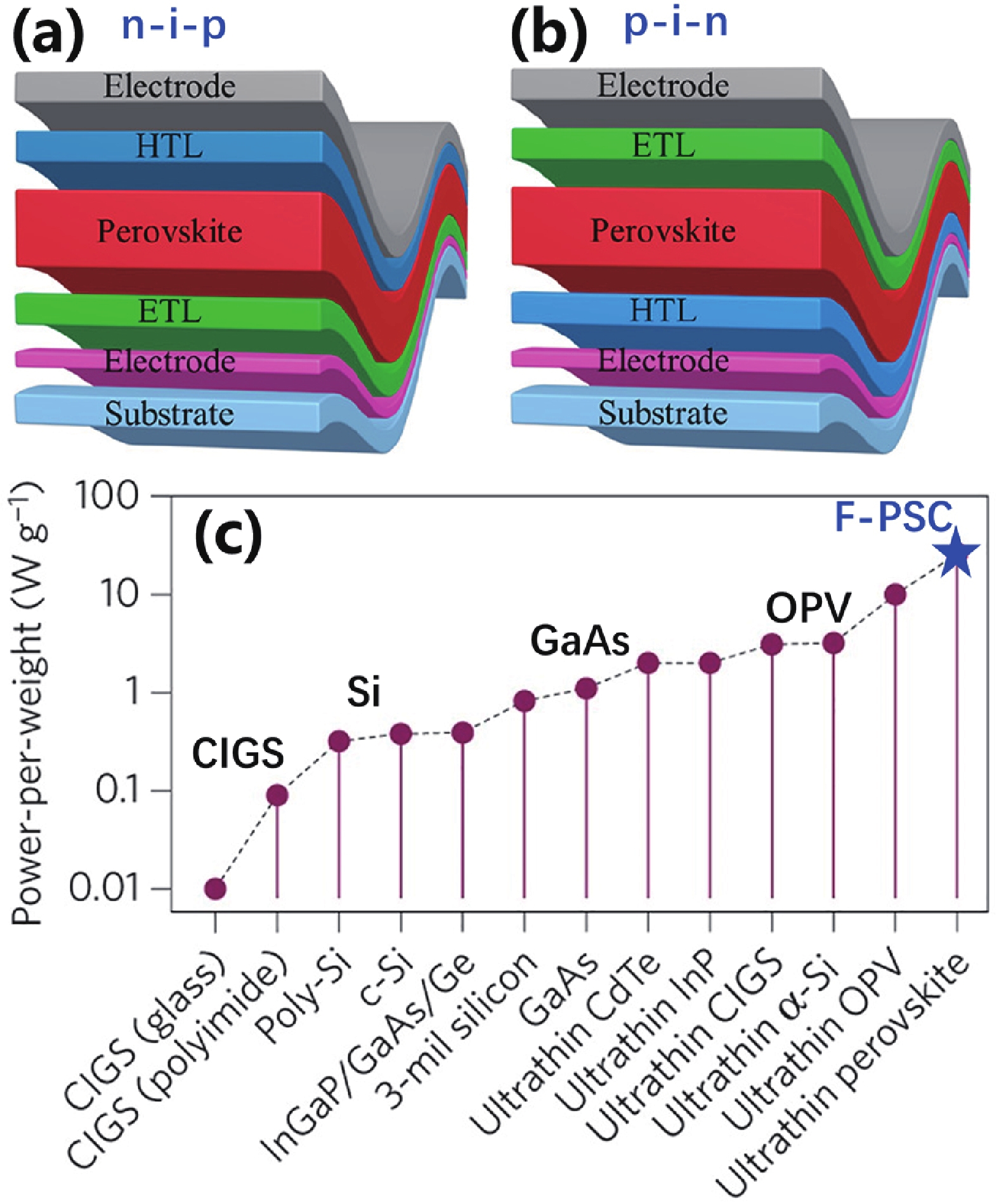
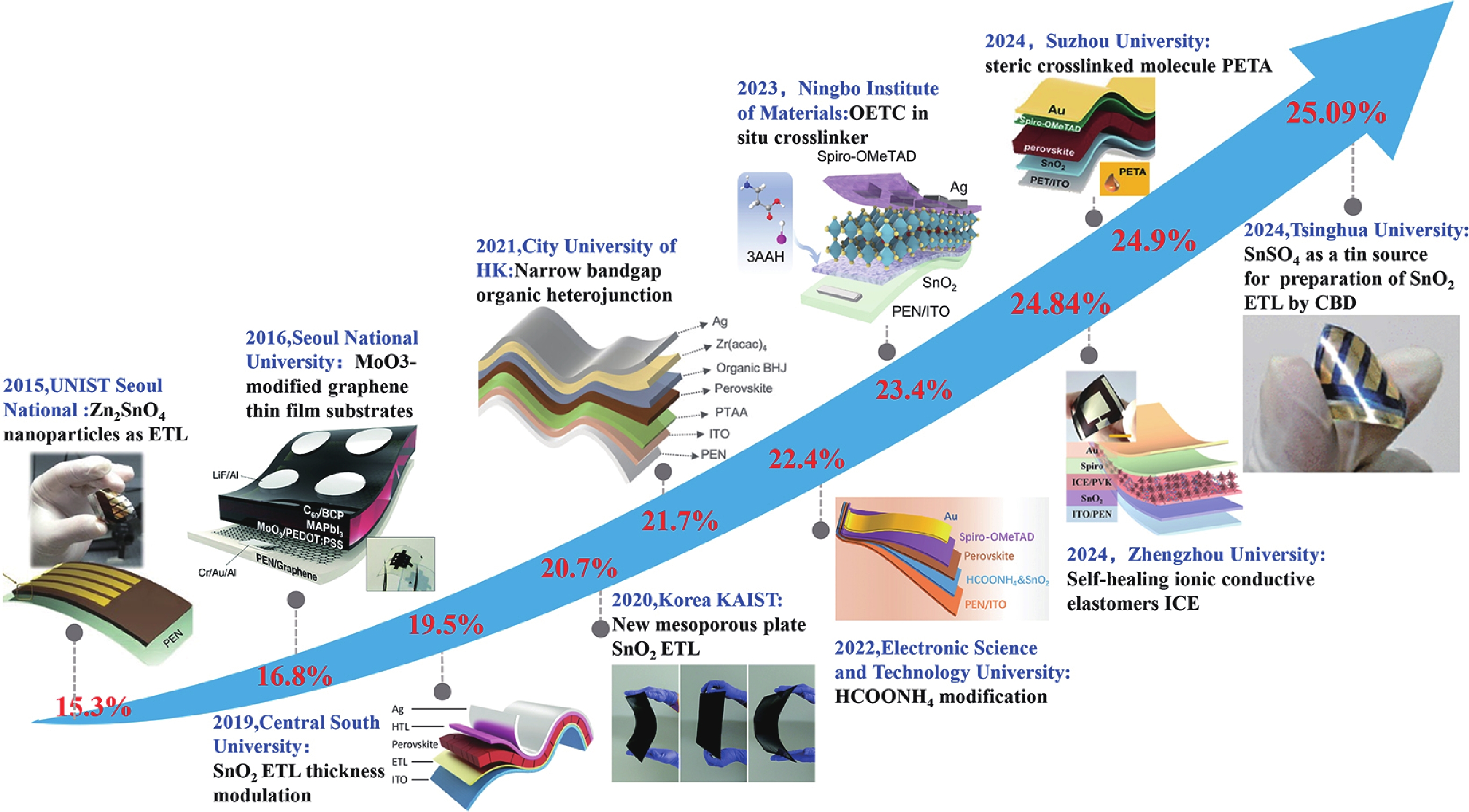
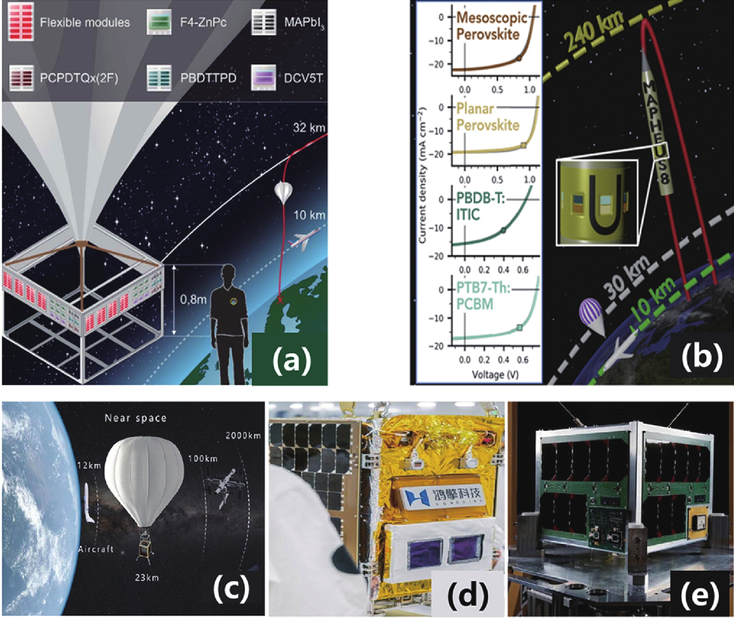
Due to advantages of high power-conversion efficiency (PCE), large power-to-weight ratio (PWR), low cost and solution processibility, flexible perovskite solar cells (f-PSCs) have attracted extensive attention in recent years. The PCE of f-PSCs has developed rapidly to over 25%, showing great application prospects in aerospace and wearable electronic devices. This review systematically sorts device structures and compositions of f-PSCs, summarizes various methods to improve its efficiency and stability recent years. In addition, the applications and potentials of f-PSCs in space vehicle and aircraft was discussed. At last, we prospect the key scientific and technological issues that need to be addressed for f-PSCs at current stage.

J. Semicond.
2025, 46(5): 051802 doi: 10.1088/1674-4926/24100034

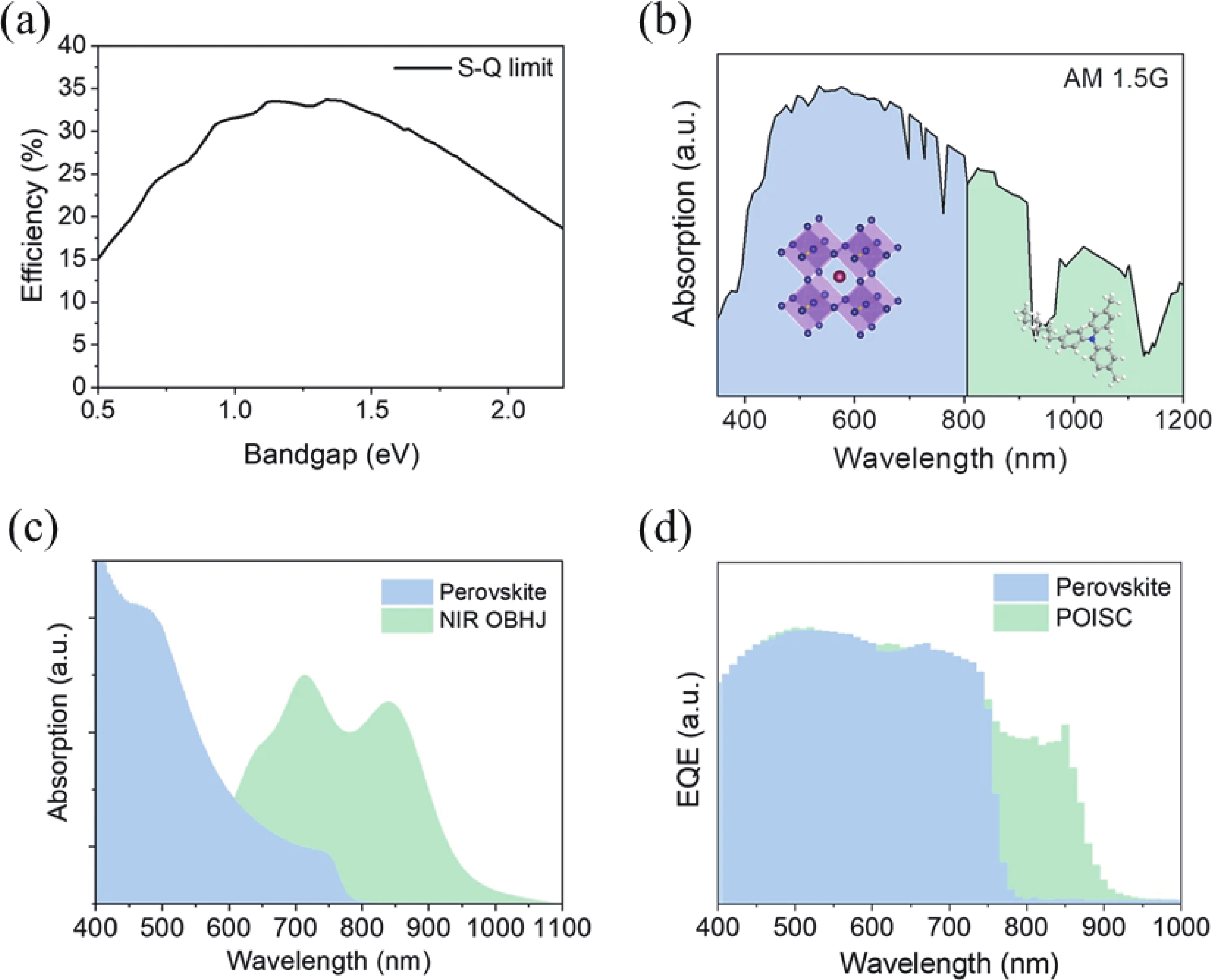
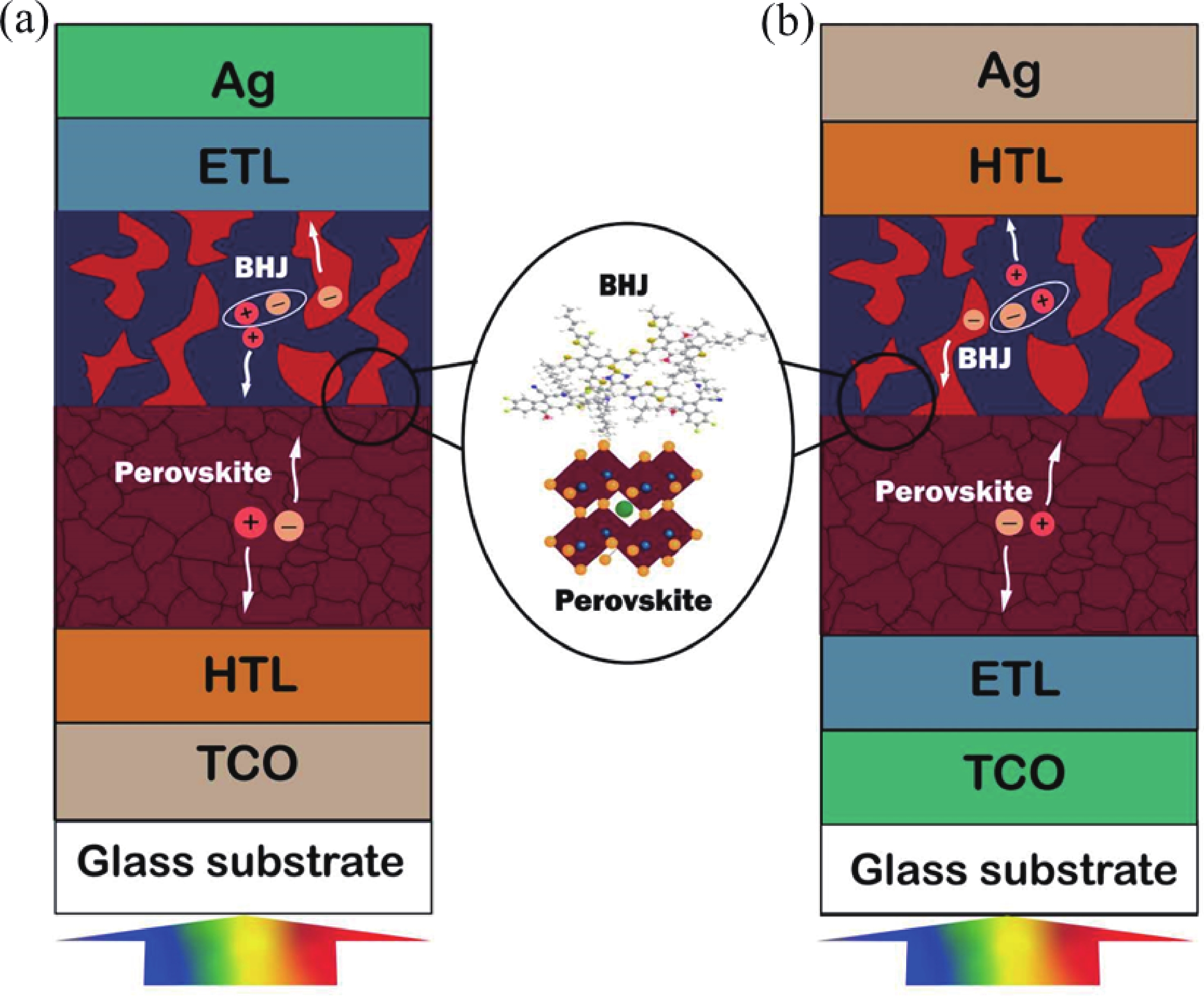
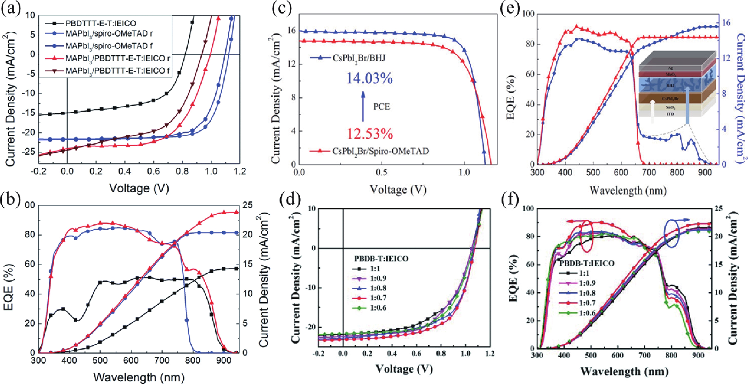
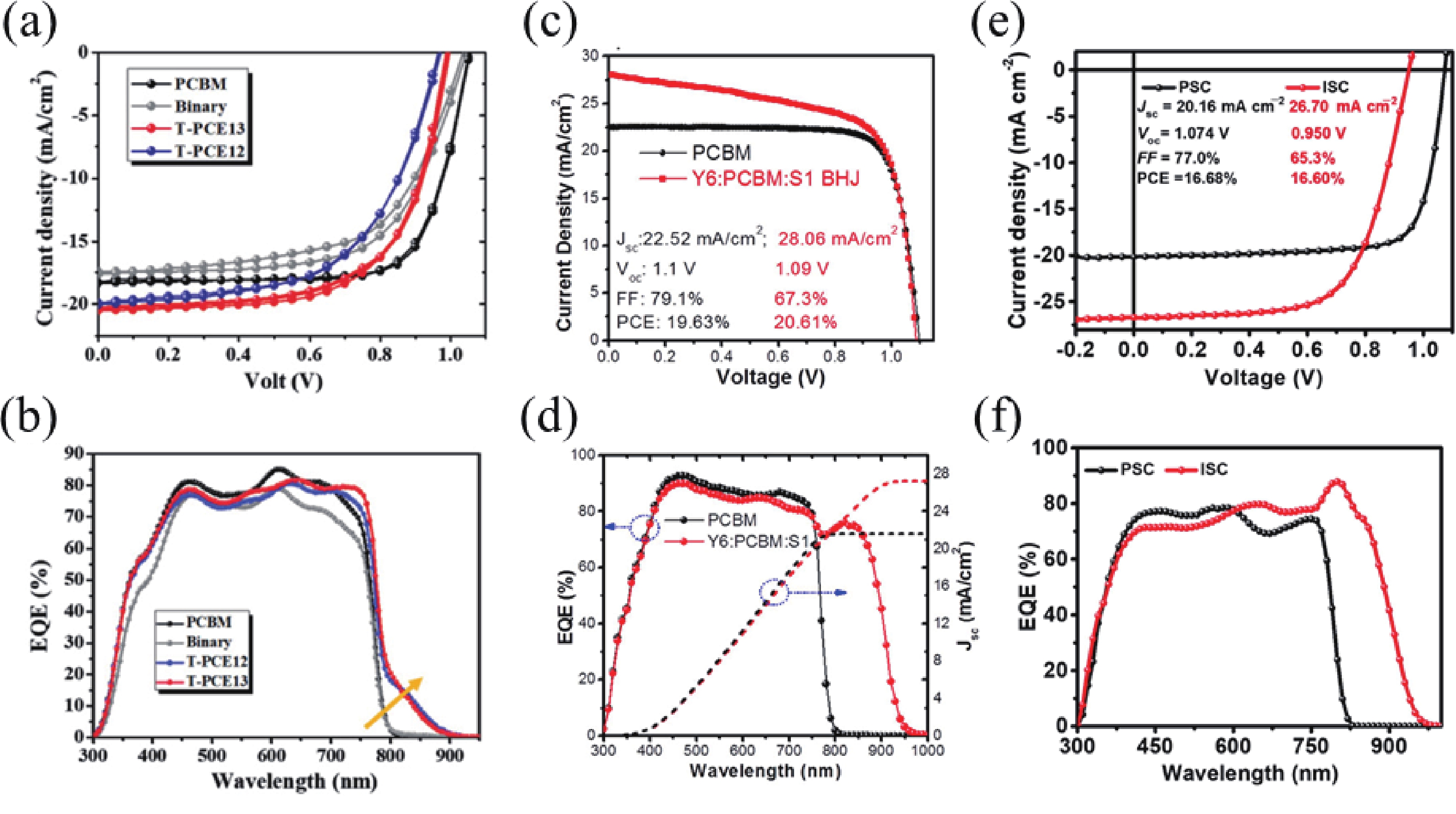
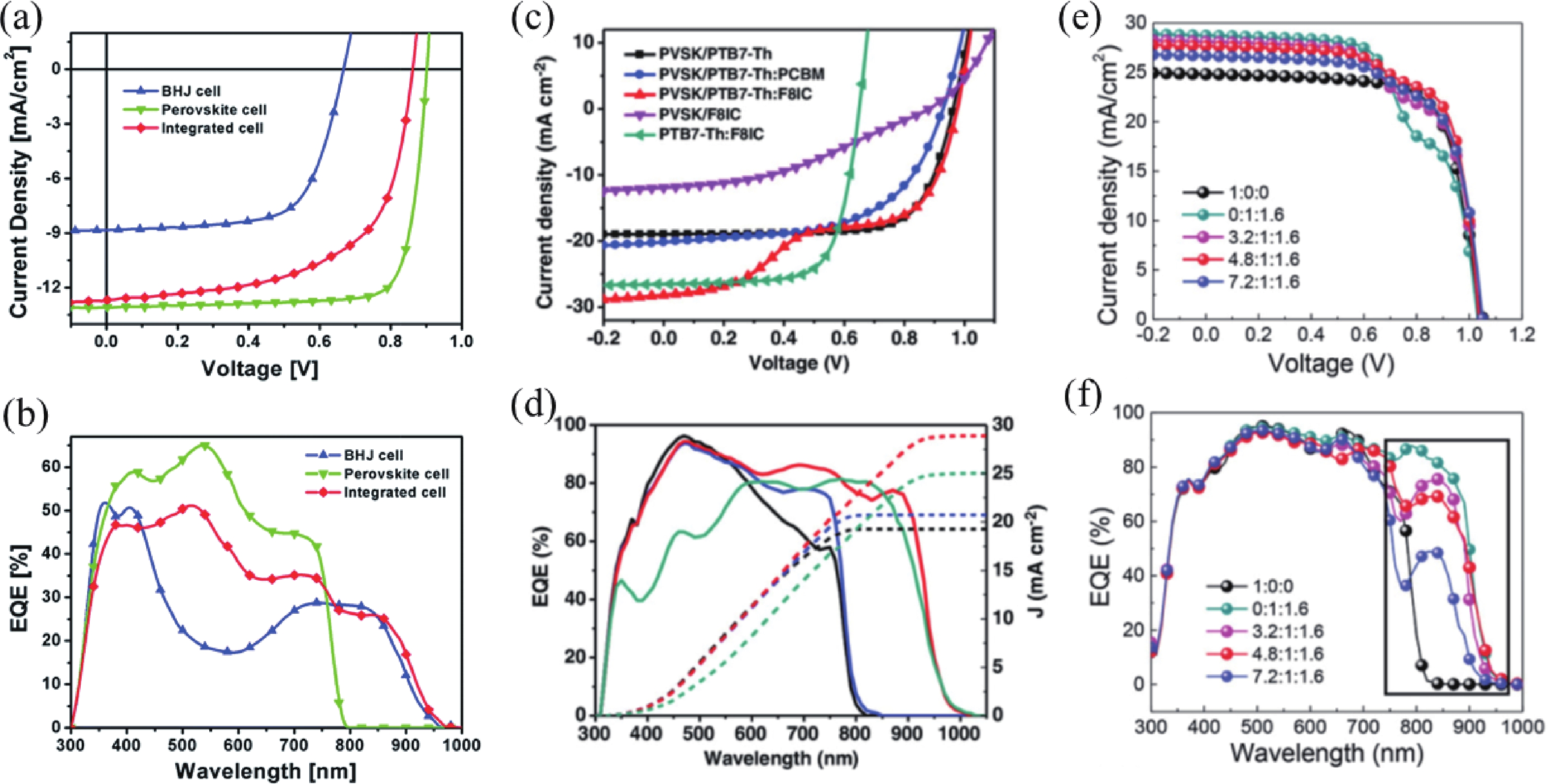
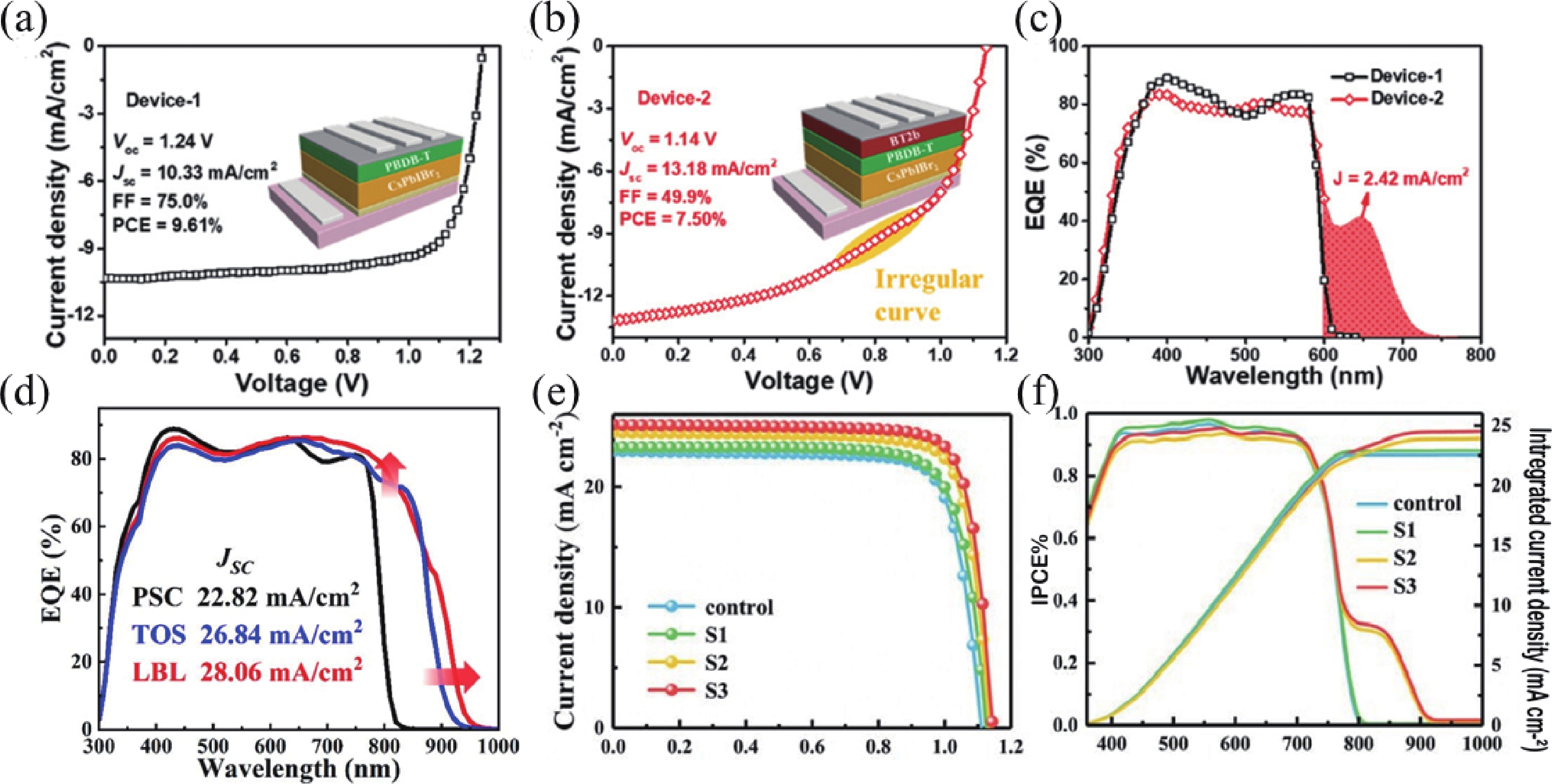
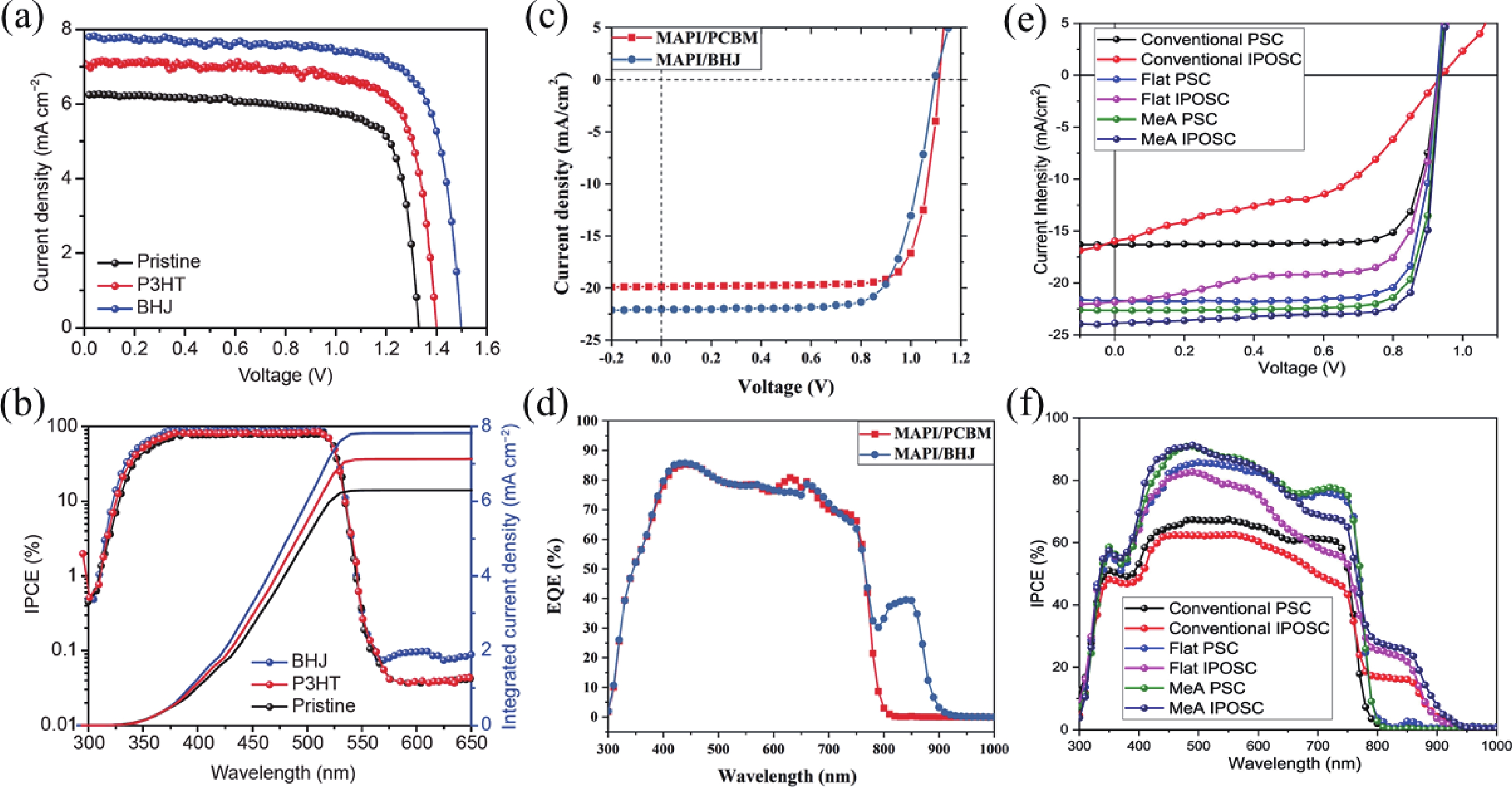
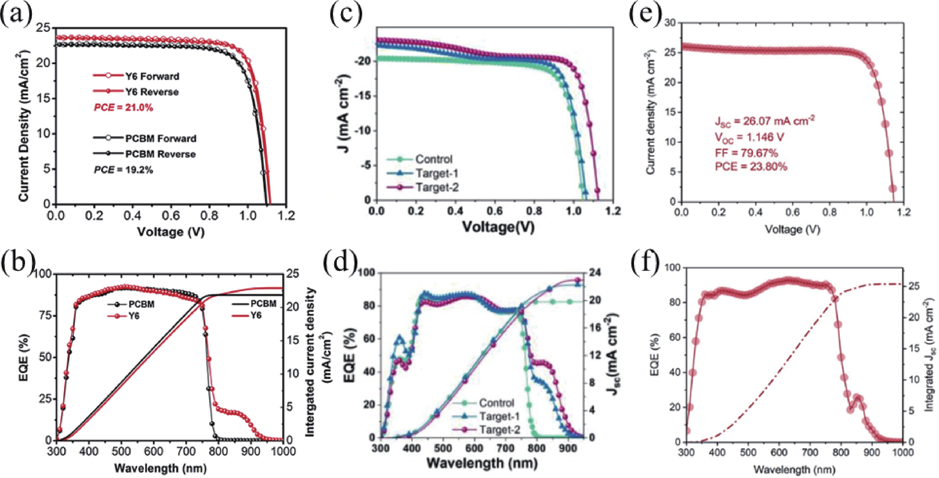
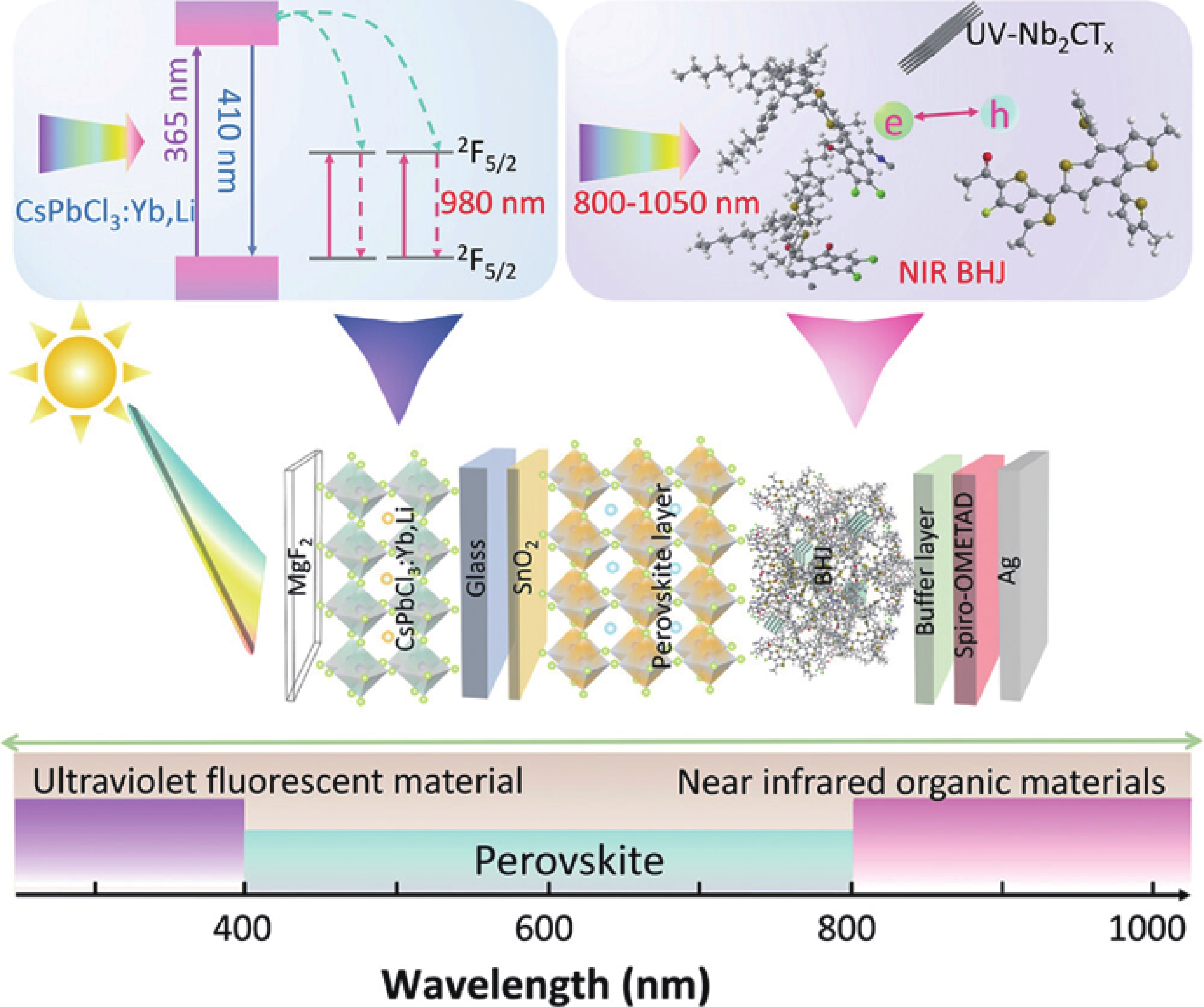
Integrated perovskite-organic solar cells (IPOSCs) offer a promising hybrid approach that combines the advantages of perovskite and organic solar cells, enabling efficient photon absorption across a broad spectrum with a simplified architecture. However, challenges such as limited charge mobility in organic bulk heterojunction (BHJ) layers, and energy-level mismatch at the perovskite/BHJ interface still sustain. Recent advancements in non-fullerene acceptors (NFAs), interfacial engineering, and emerging materials have improved charge transfer/transport, and overall power conversion efficiency (PCE) of IPOSCs. This review explores key developments in IPOSCs, focusing on low-bandgap materials for near-infrared absorption, energy alignment optimization, and strategies to enhance photocurrent density and device performance. Future innovations in material selection and device architecture will be crucial for further improving the efficiency of IPOSCs, bringing them closer to practical application in next-generation photovoltaic technologies.


J. Semicond.
2025, 46(5): 051803 doi: 10.1088/1674-4926/24100032

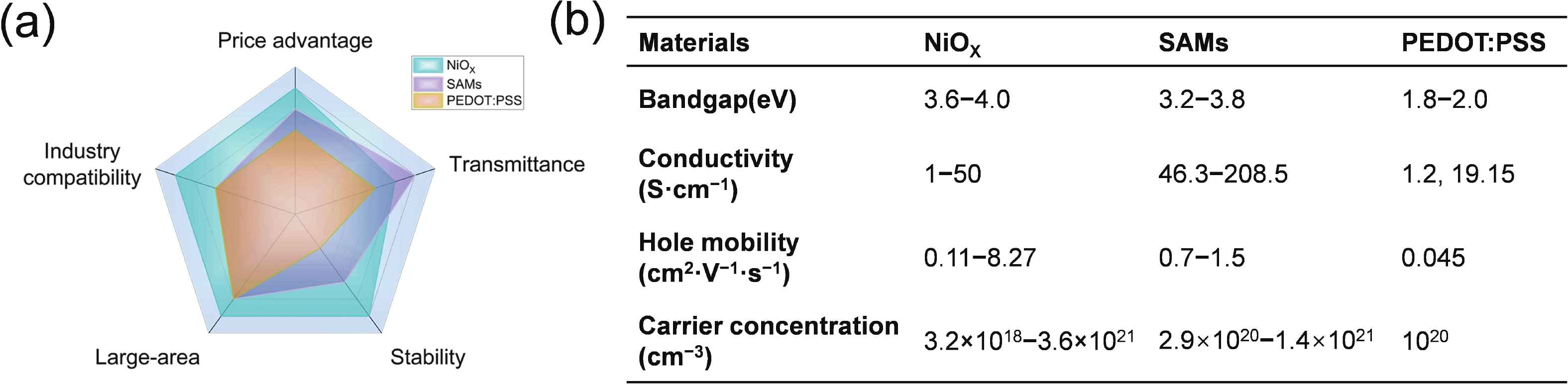
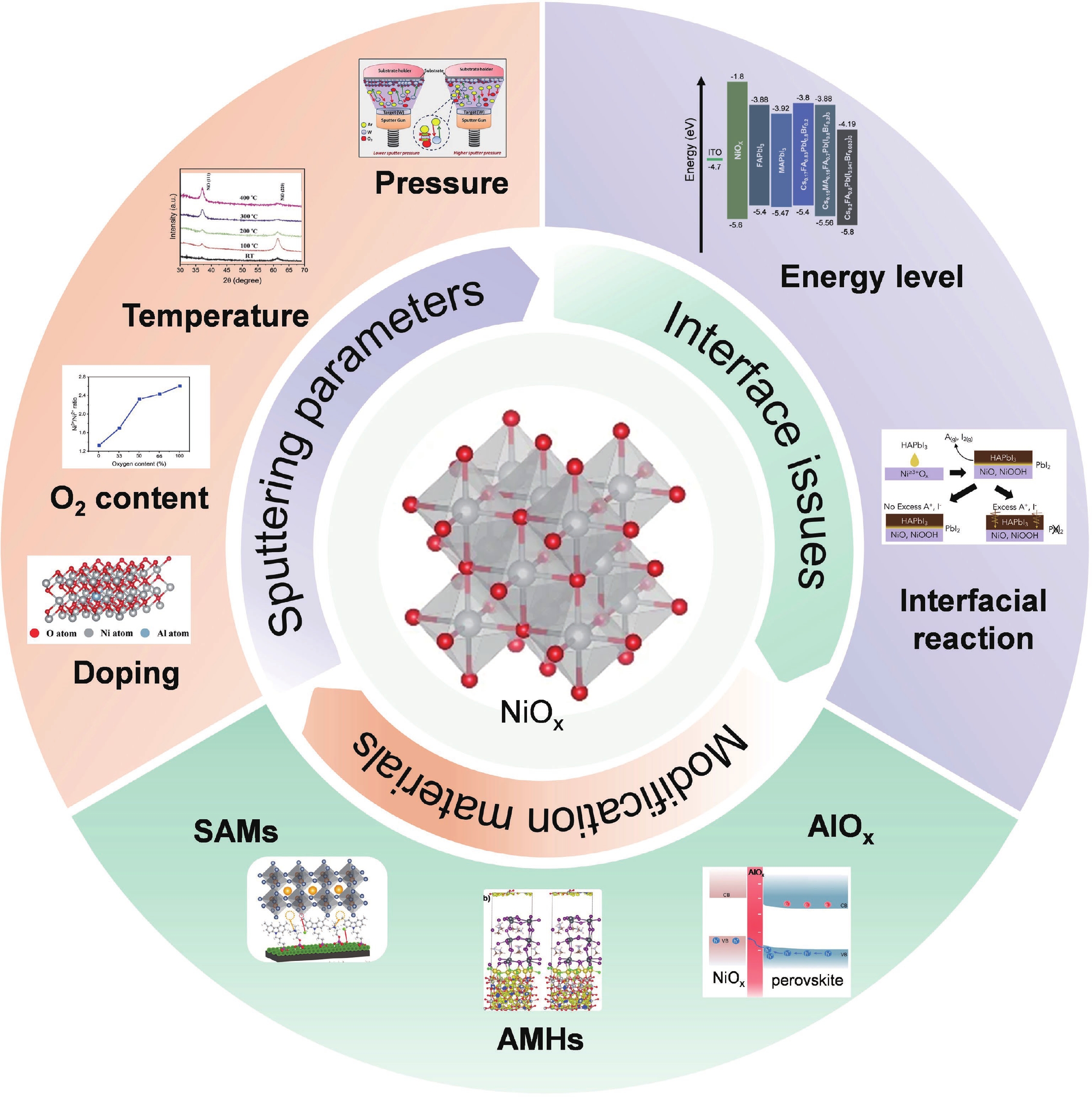
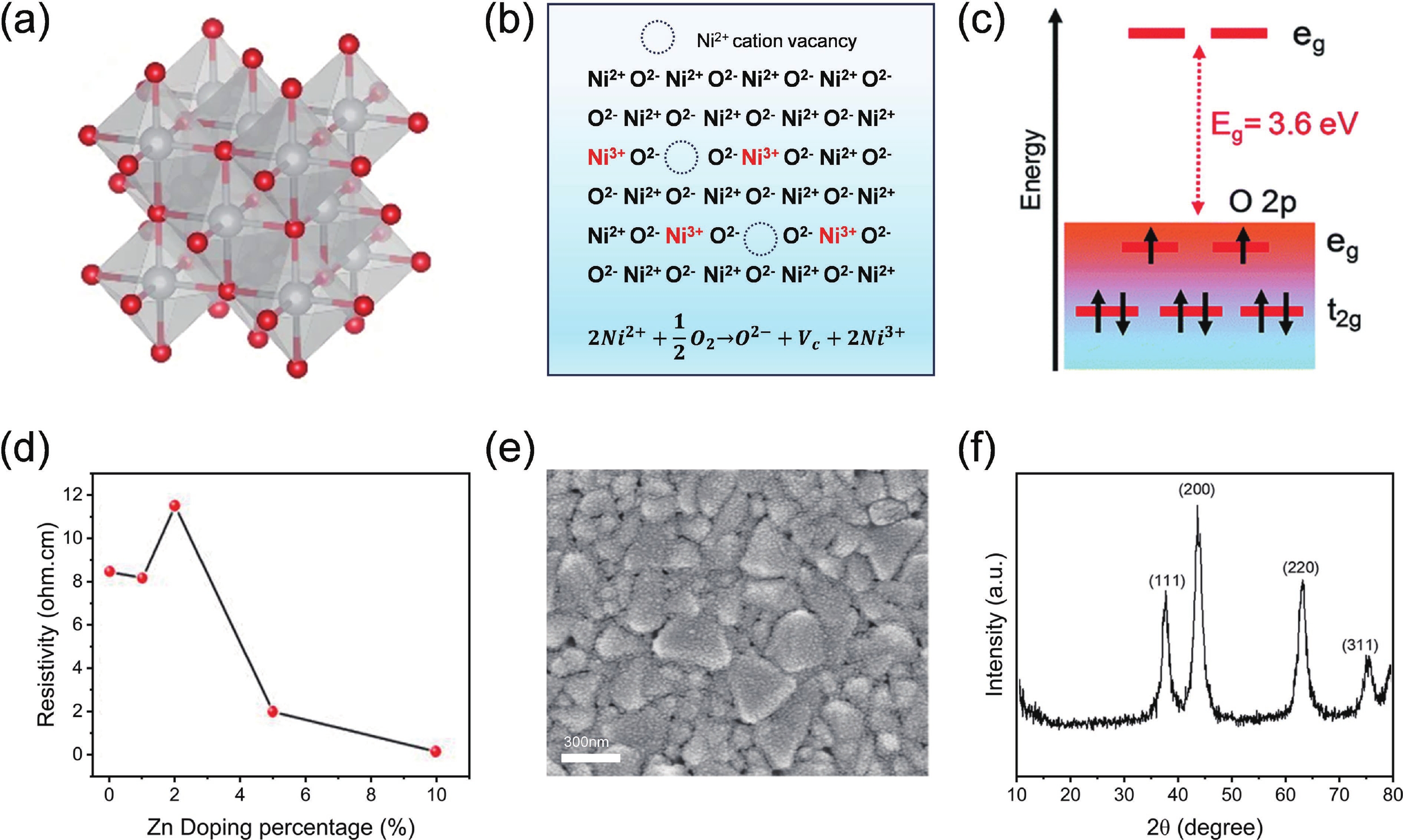
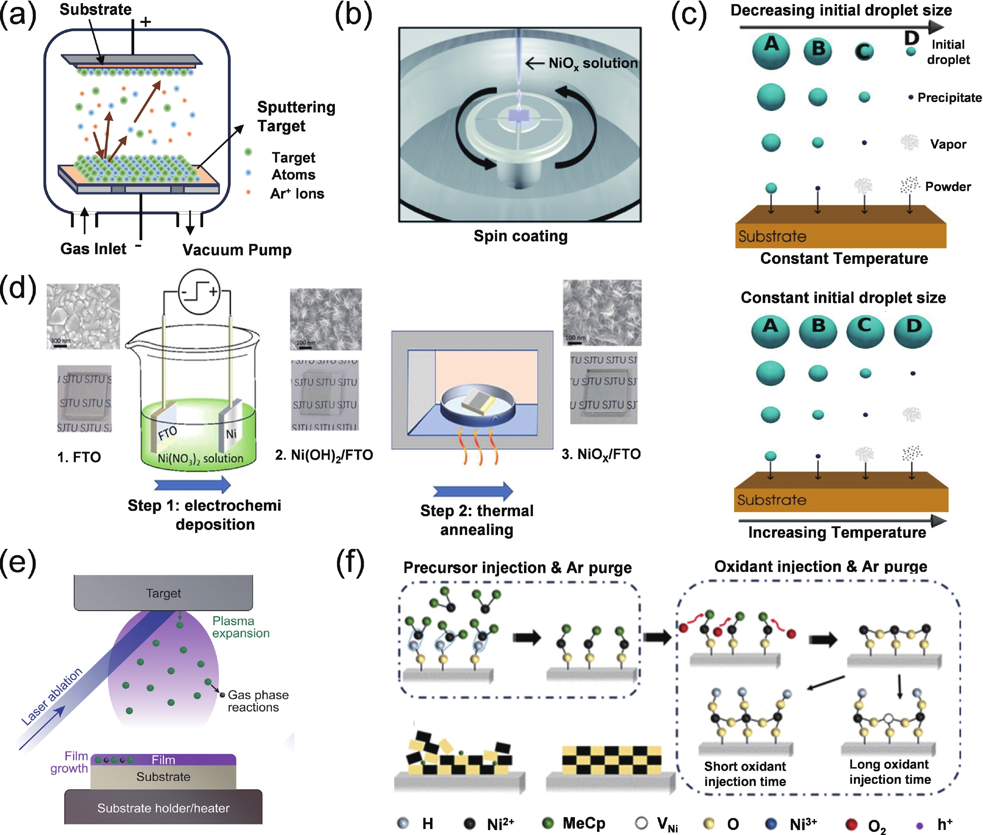
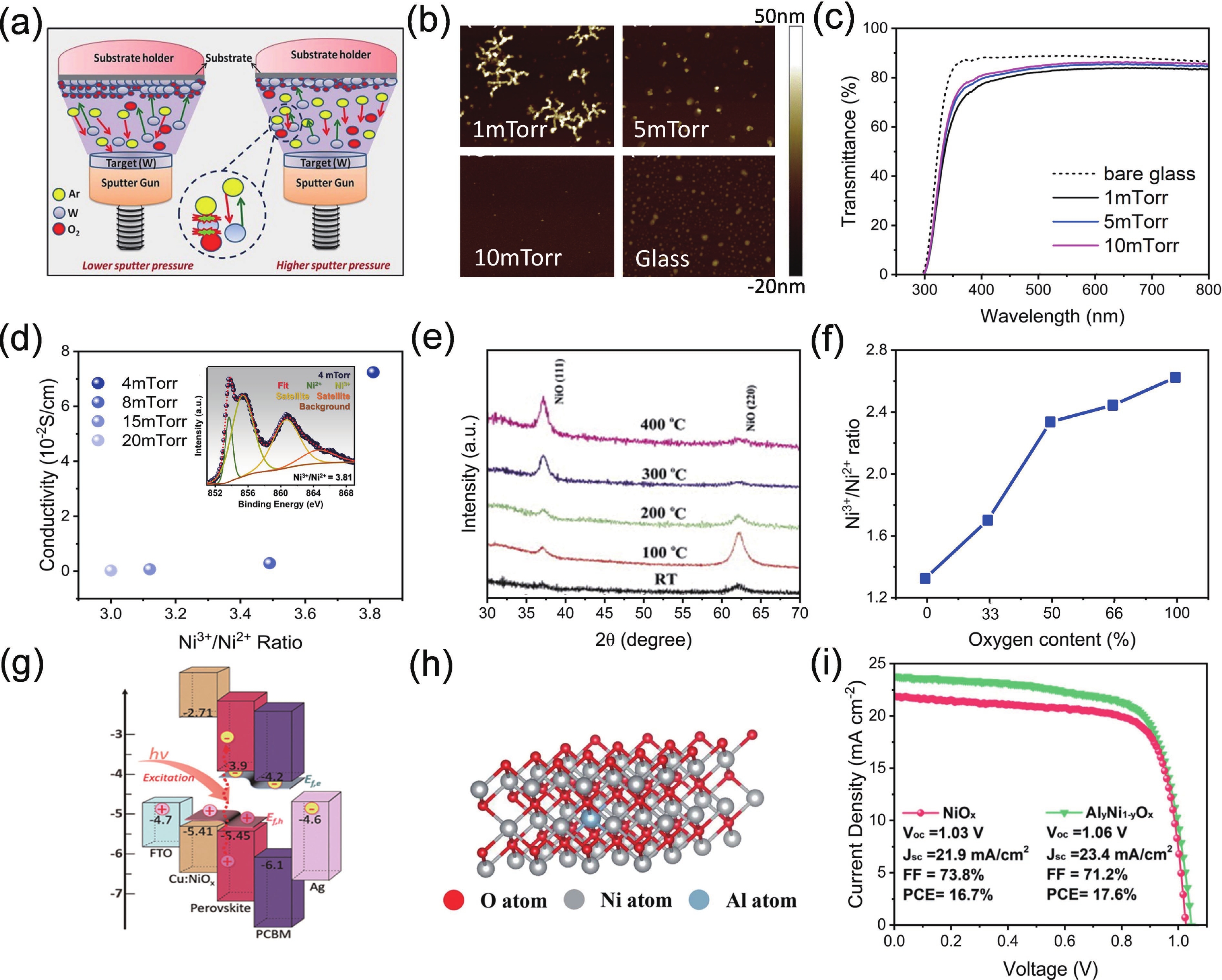
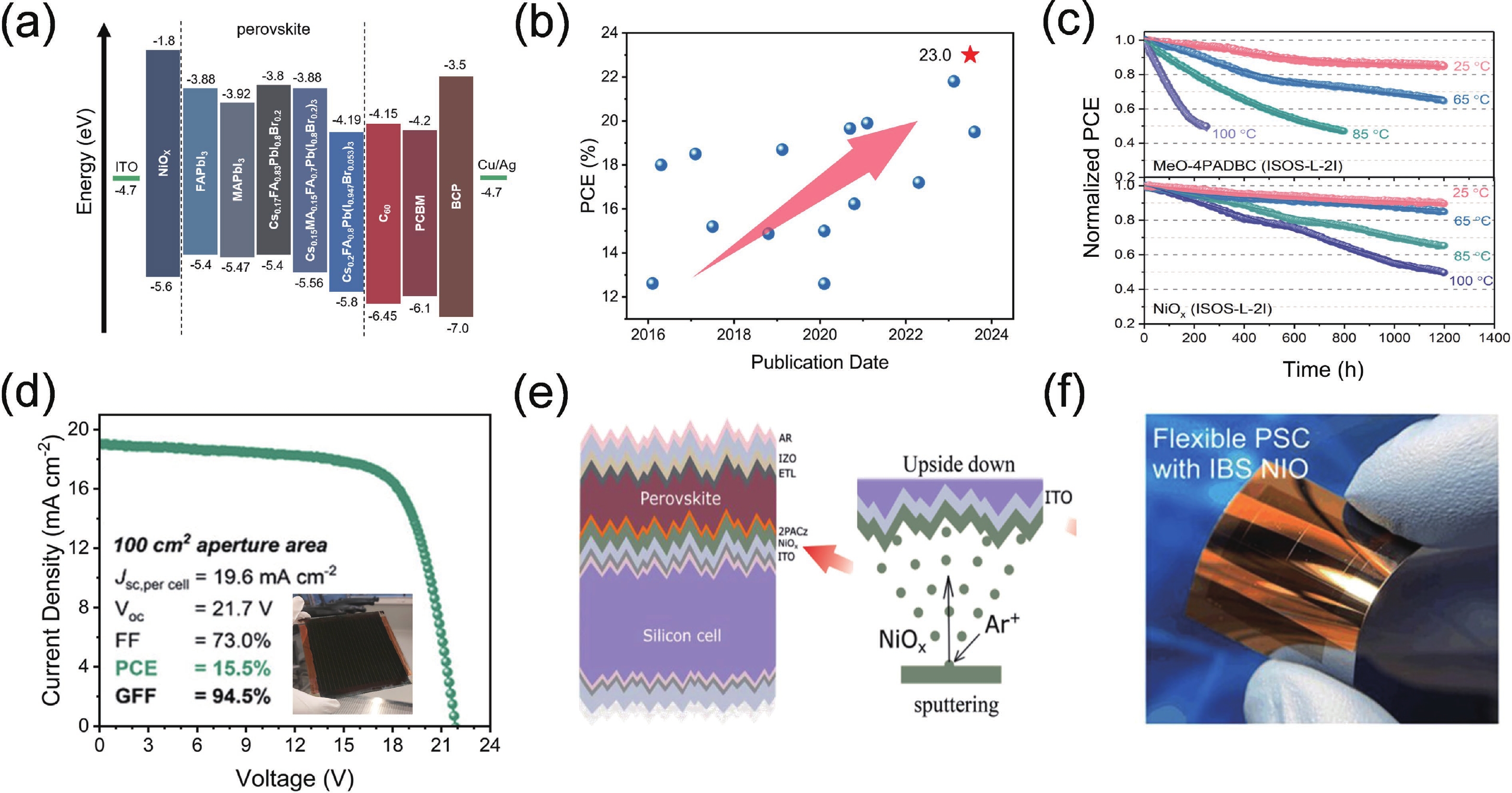
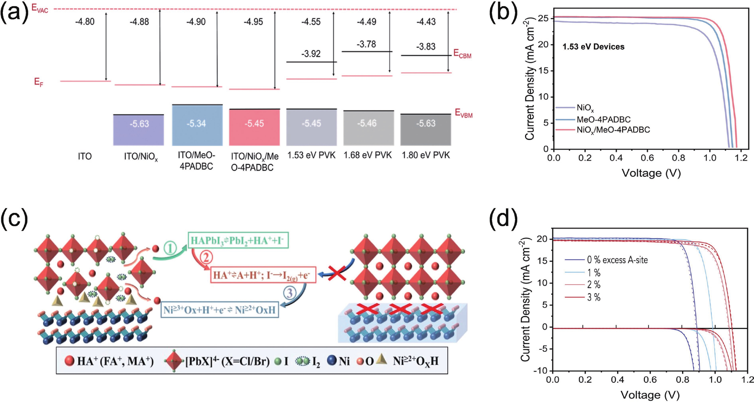
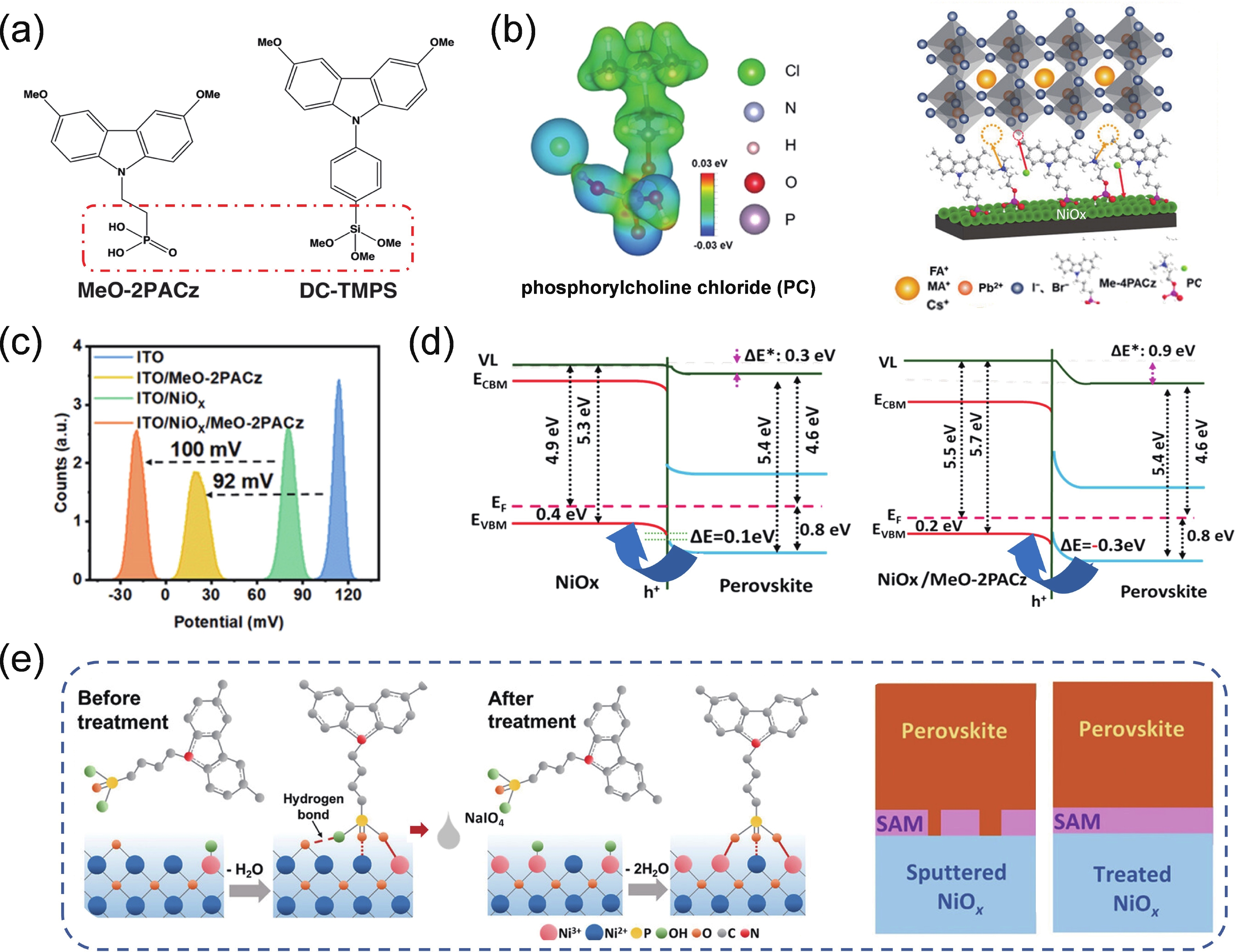
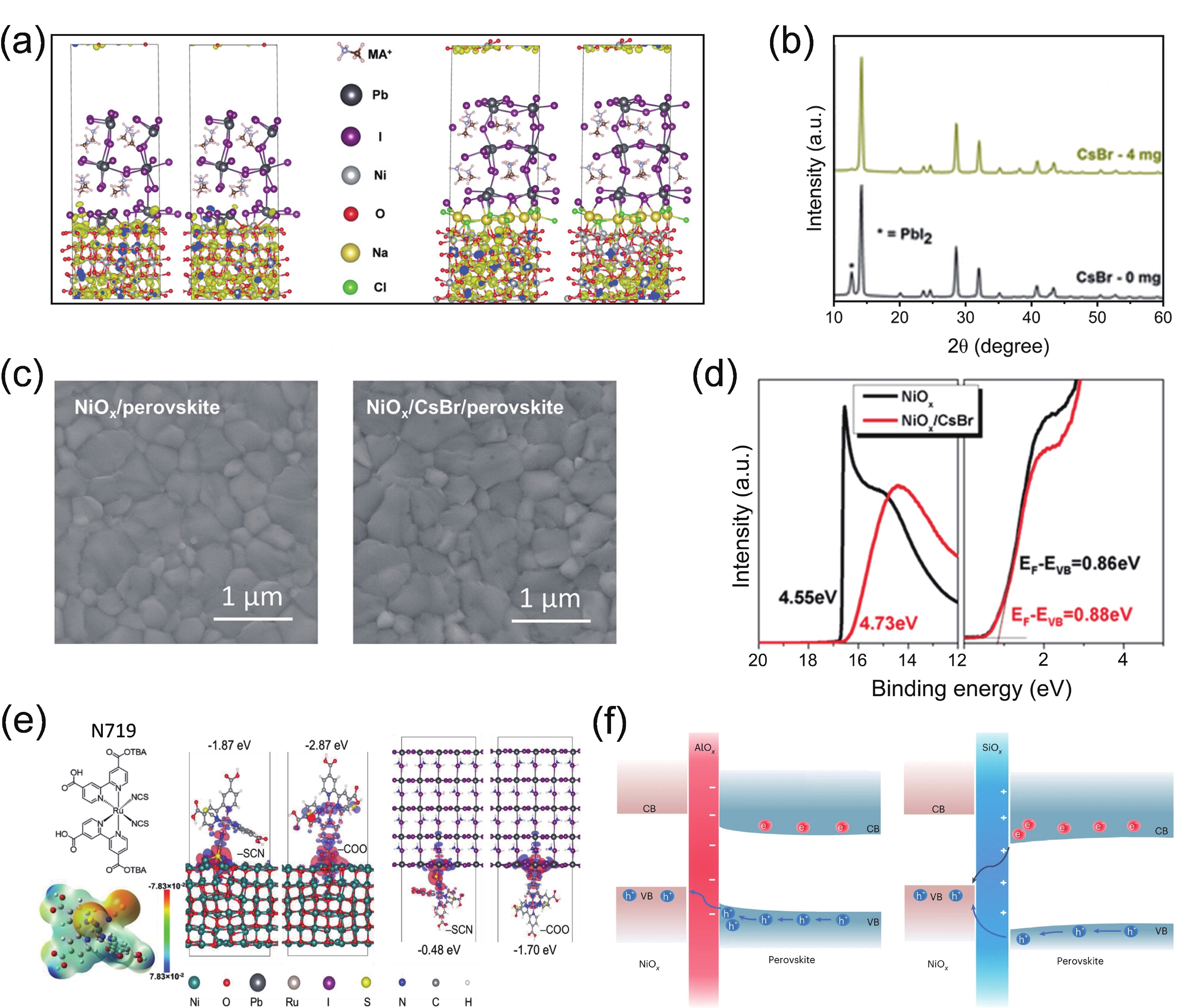
Perovskite solar cells (PSCs) have become a hot topic in the field of renewable energy due to their excellent power conversion efficiency and potential for low-cost manufacturing. The hole transport layer (HTL), as a key component of PSCs, plays a crucial role in the cell's overall performance. Magnetron sputtering NiOx has attracted widespread attention due to its high carrier mobility, excellent stability, and suitability for large-scale production. Herein, an insightful summary of the recent progress of magnetron sputtering NiOx as the HTL of PSCs is presented to promote its further development. This review summarized the basic properties of magnetron sputtering NiOx thin film, the key parameters affecting the optoelectronic properties of NiOx thin films during the magnetron-sputtering process, and the performance of the corresponding PSCs. Special attention was paid to the interfacial issues between NiOx and perovskites, and the modification strategies were systematically summarized. Finally, the challenges of sputtering NiOx technology and the possible development opportunities were concluded and discussed.
J. Semicond.
2025, 46(5): 051804 doi: 10.1088/1674-4926/24100024

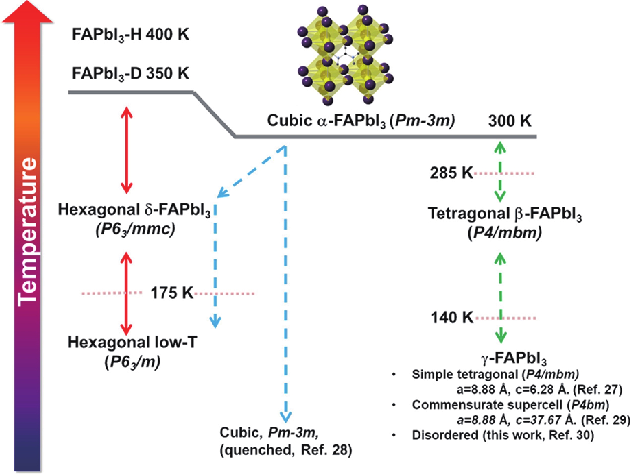
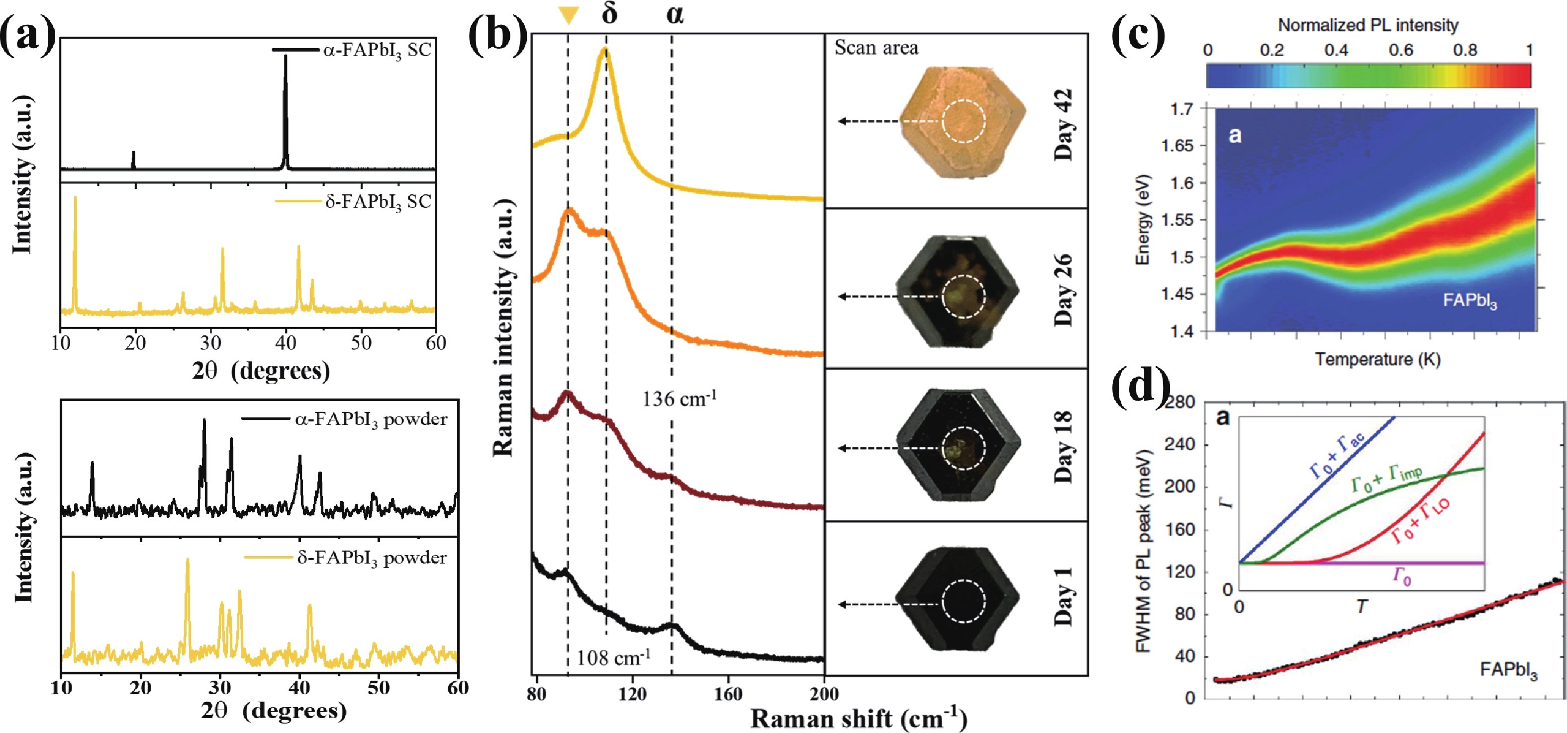
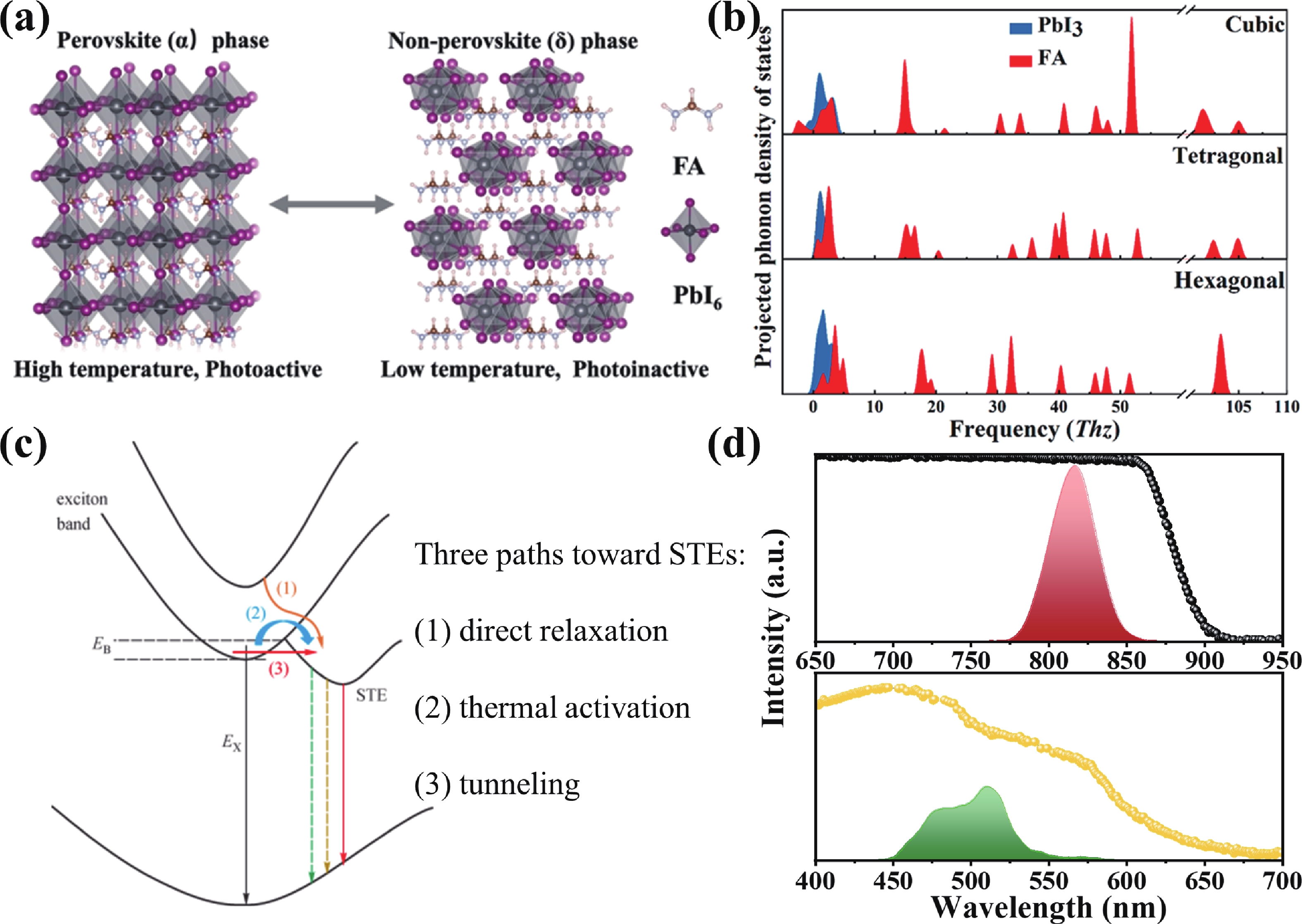
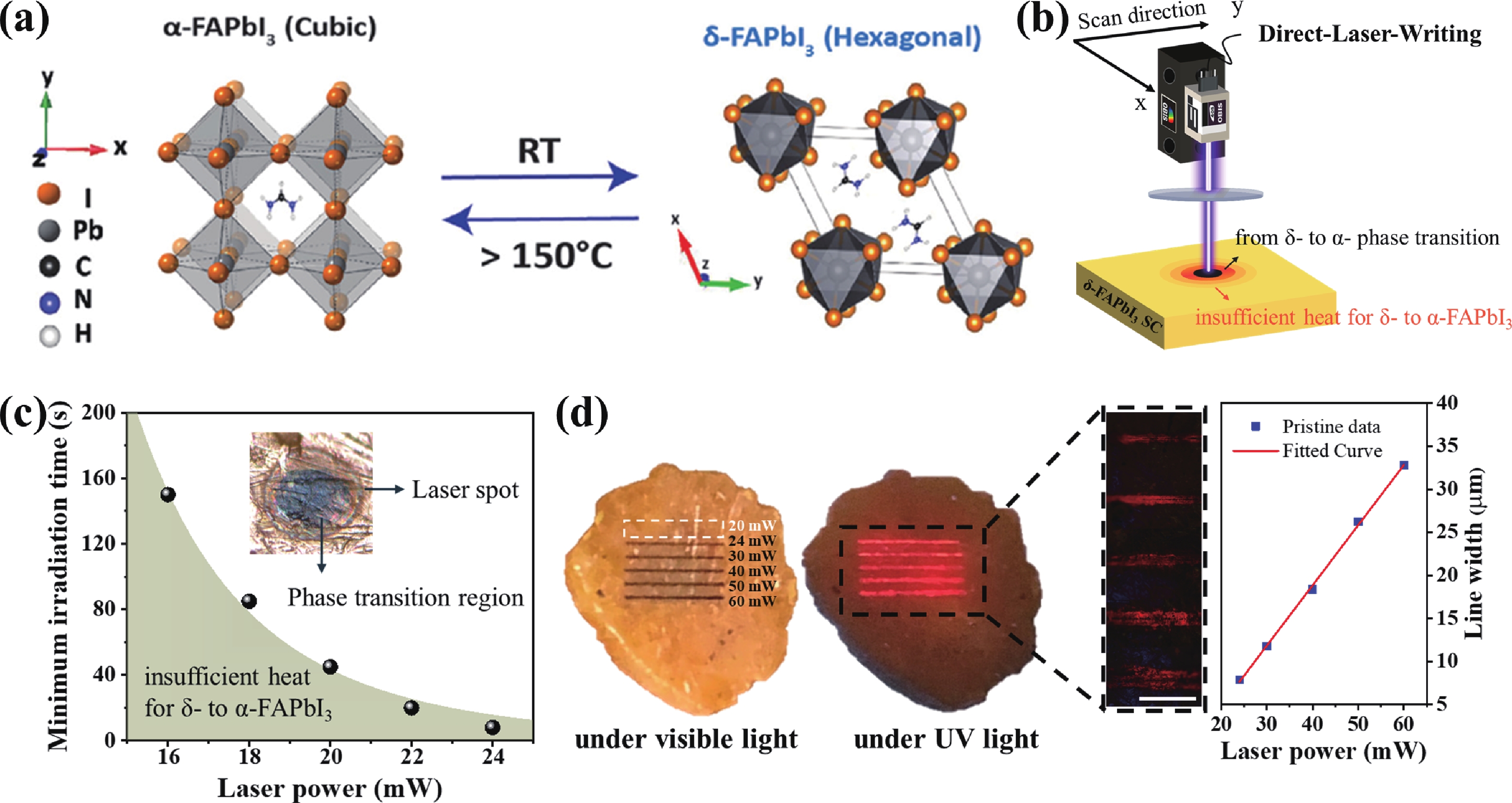
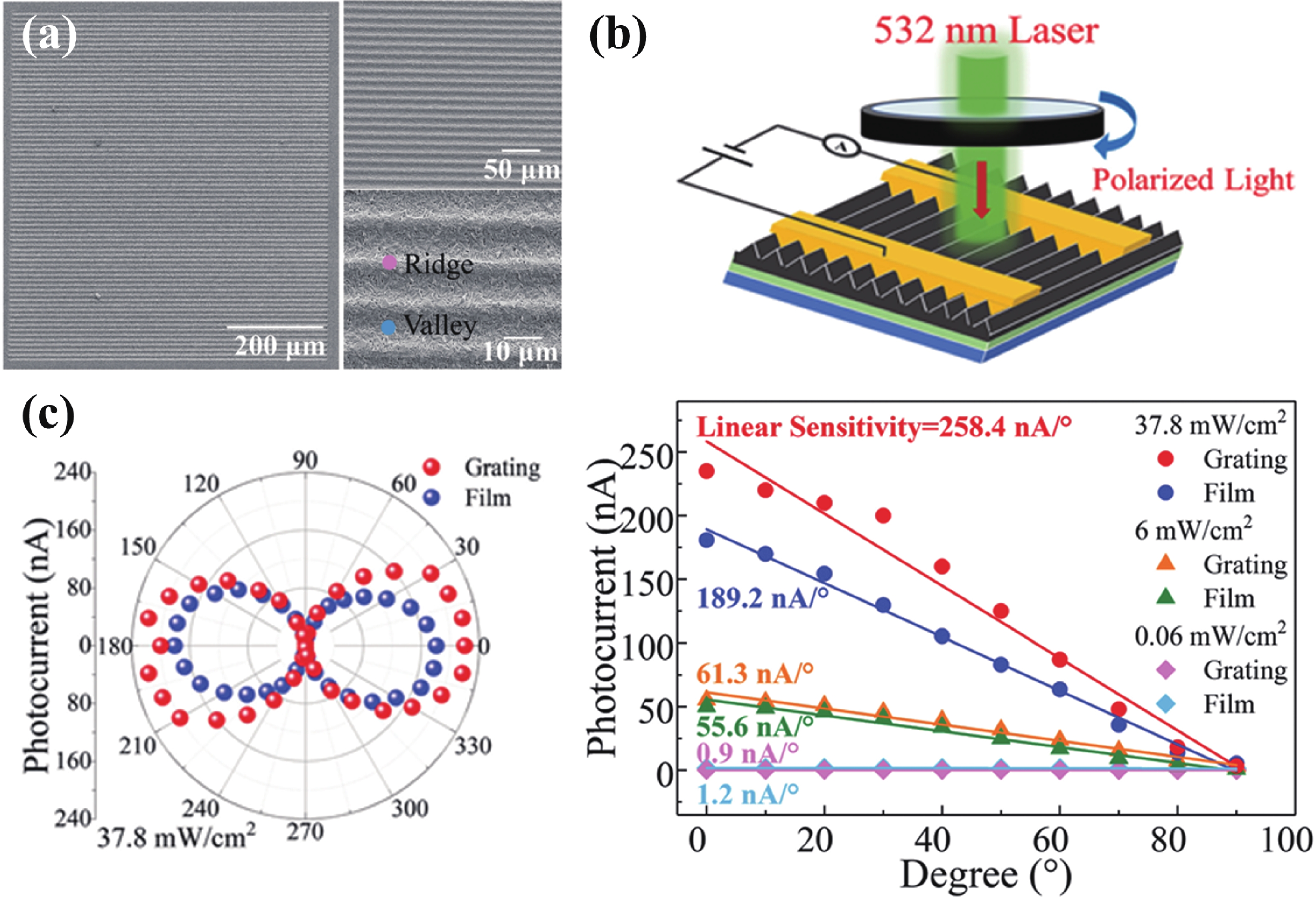
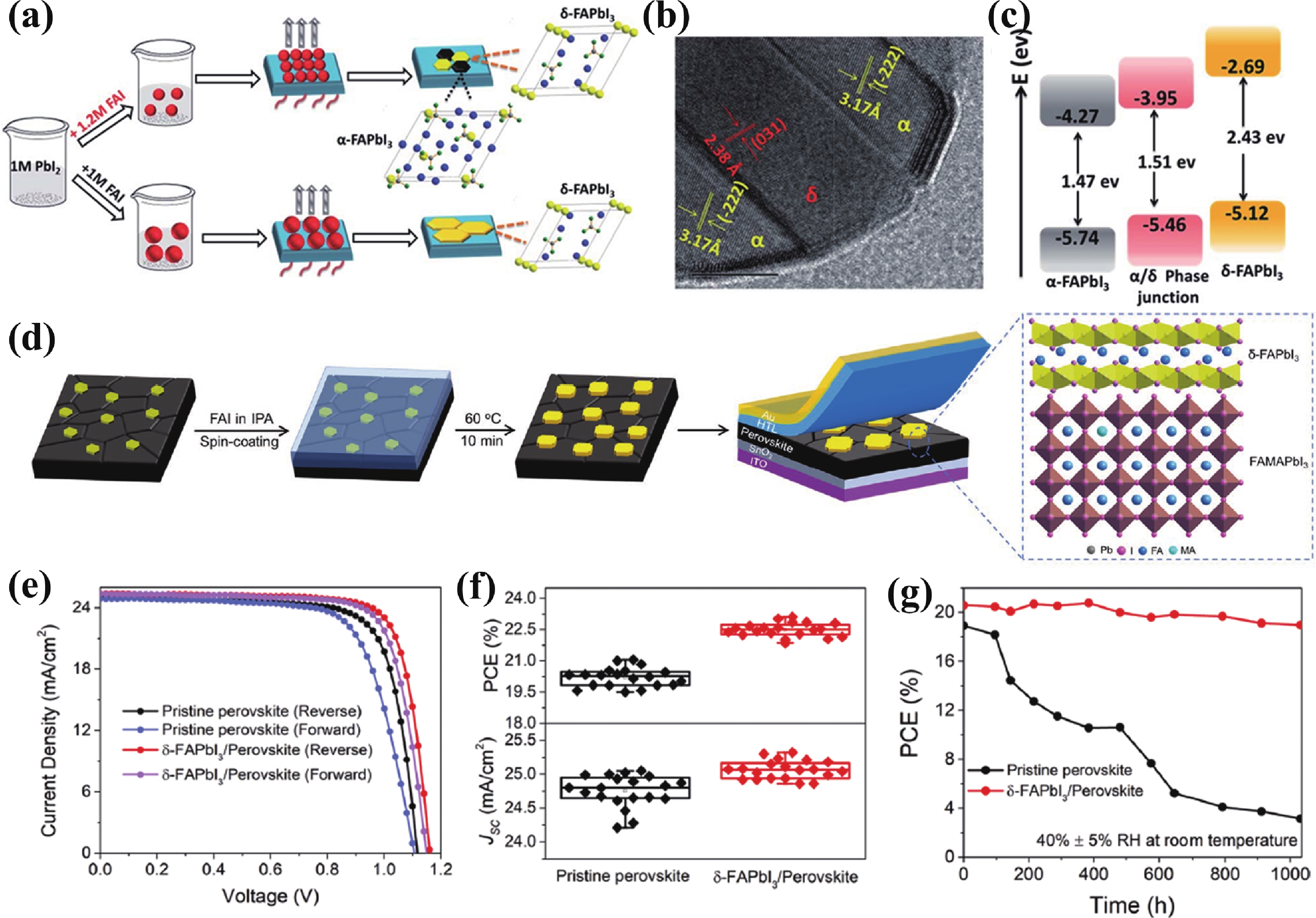
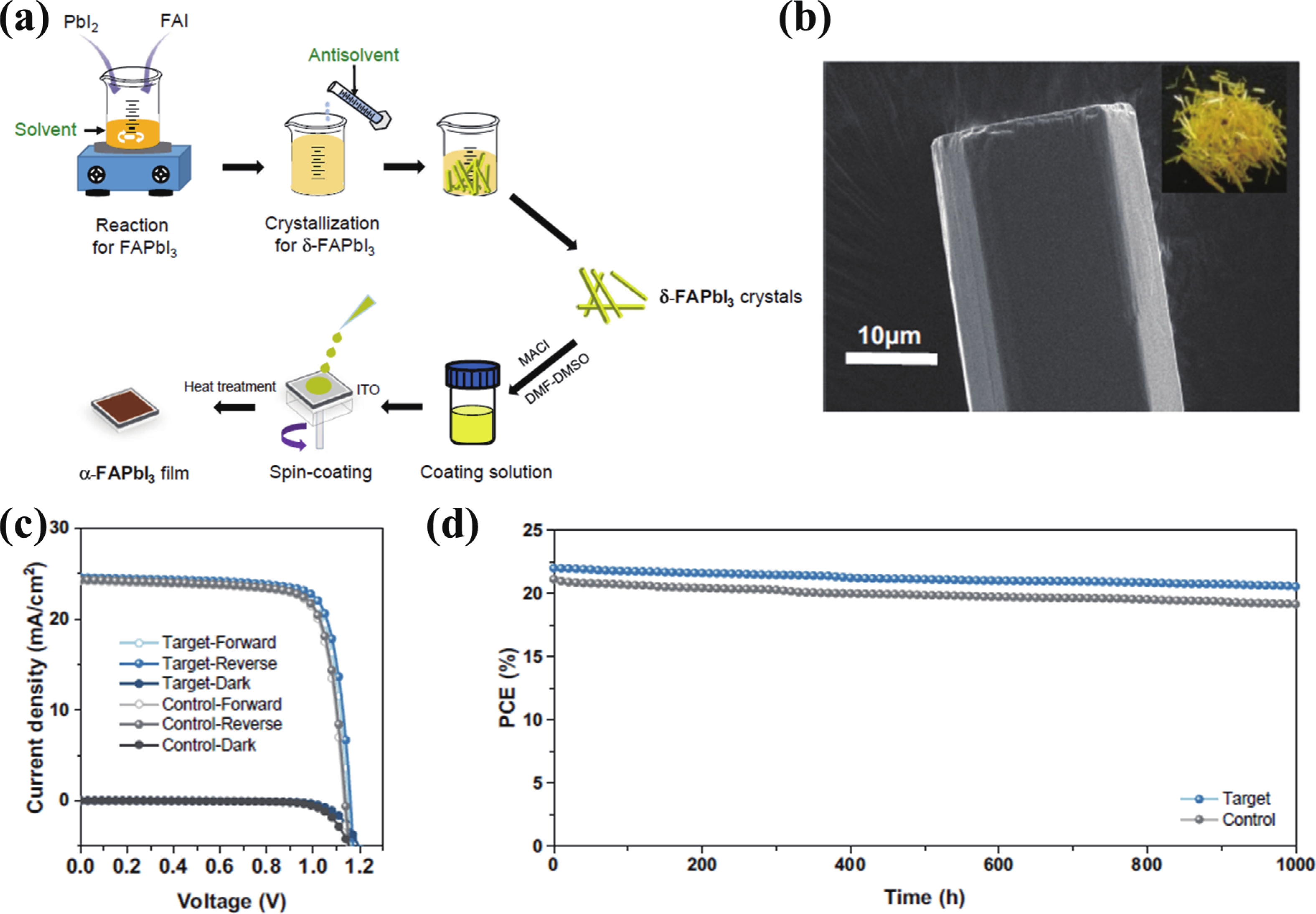
Halide perovskites have attracted great interest as active layers in optoelectronic devices. Among perovskites with diverse compositions, α-FAPbI3 is of utmost importance with great optoelectronic properties and a decent bandgap of 1.48 eV. However, the α-phase suffers an irreversible transition to the photo-inactive δ-phase, whereas the δ-phase is usually regarded as useless phase with poor optoelectronic properties. Therefore, it is commonly accepted that the thermodynamic stable δ-FAPbI3 greatly limits the application of FAPbI3. Every coin has two sides, although the δ-phase is difficult to apply as photoelectrical active layers, it is possible to combine δ-FAPbI3 with α-FAPbI3 to realize functional applications. Firstly, this review analyzes the cause of the contrasting properties between α- and δ-FAPbI3, where the stronger electron−phonon coupling in 1D hexagonal δ-FAPbI3 restricts its internal carrier and phonon transport. Secondly, the factors affecting the phase transitions and strategies to control phase transition between α- and δ-FAPbI3 are presented. Finally, some functional applications of δ-FAPbI3 in combination with α-FAPbI3 are given according to previous reports. By and large, we hope to introduce δ-FAPbI3 from another perspective and give some insights into its unique properties, hopefully providing new strategies for the subsequent advances to FAPbI3.


J. Semicond.
2025, 46(5): 052801 doi: 10.1088/1674-4926/24110016
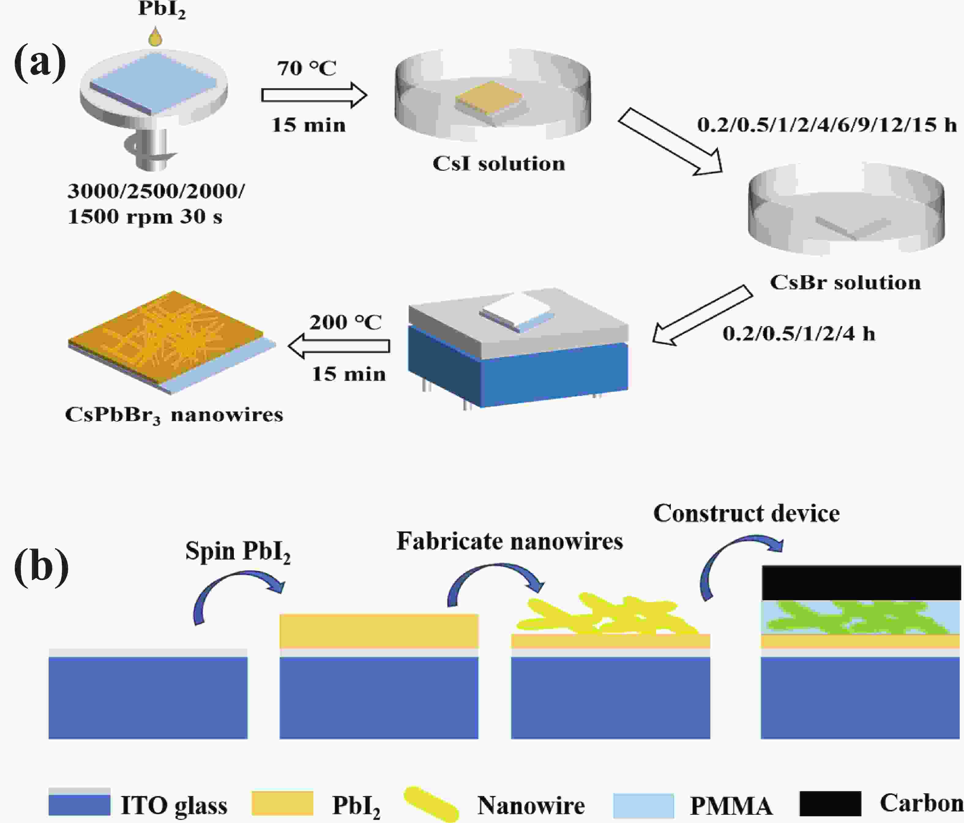
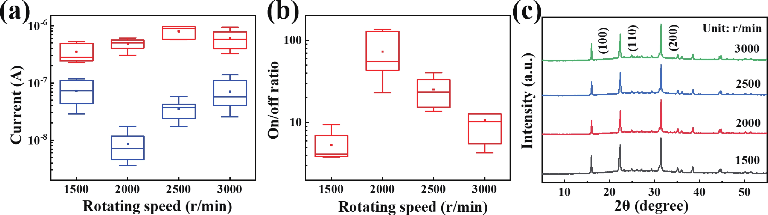
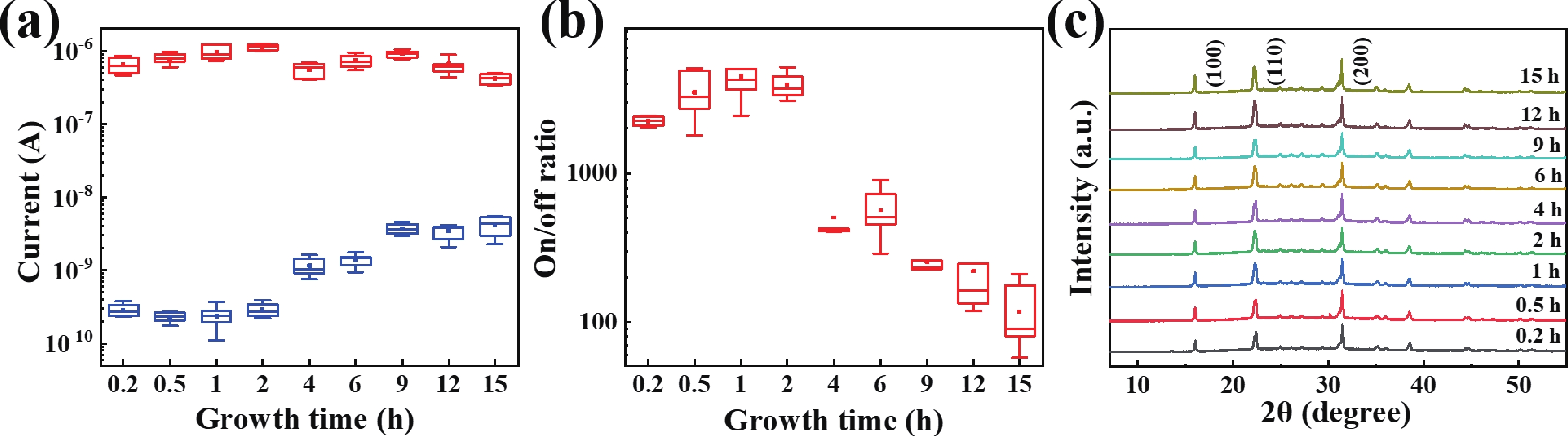
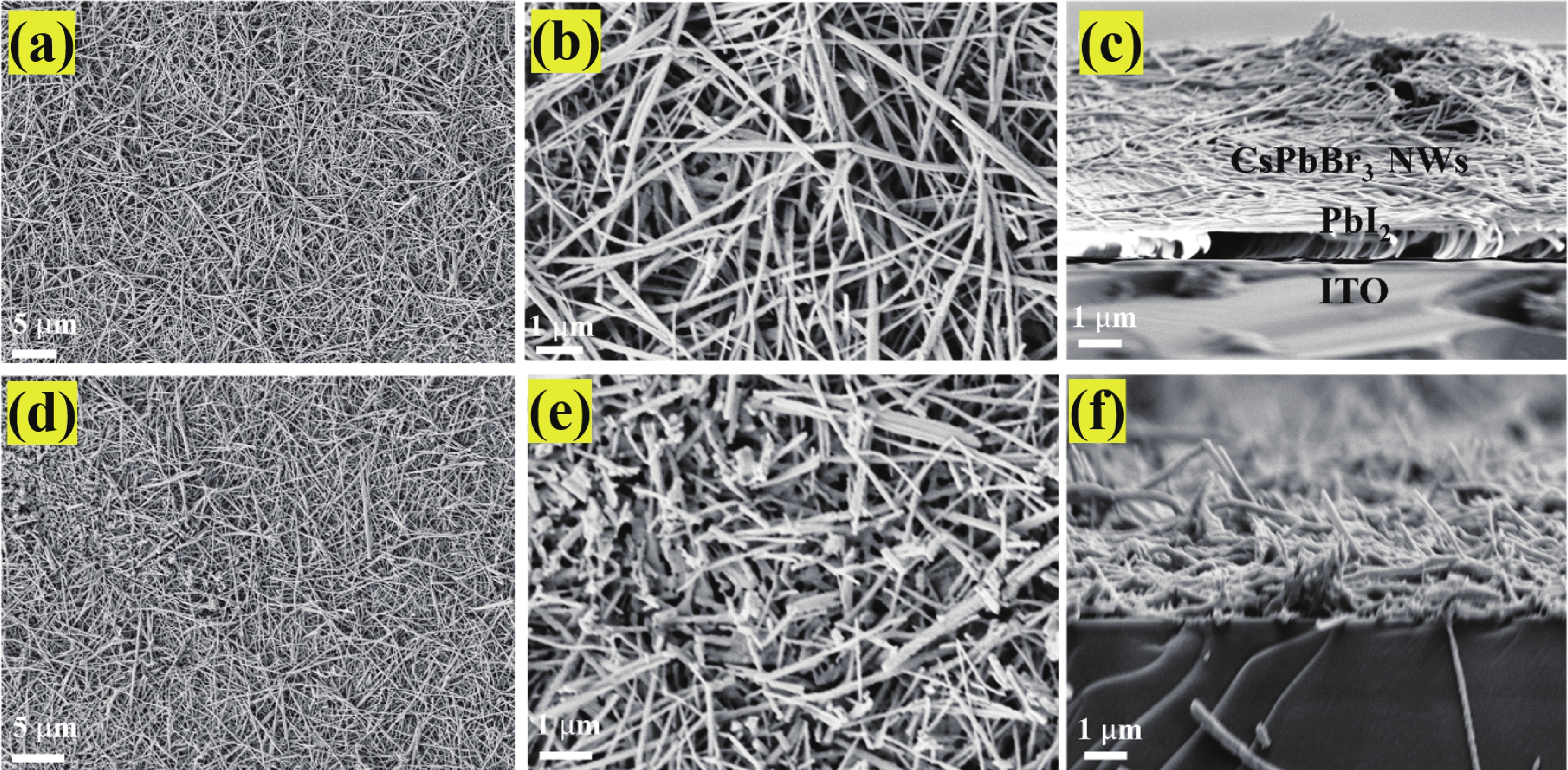
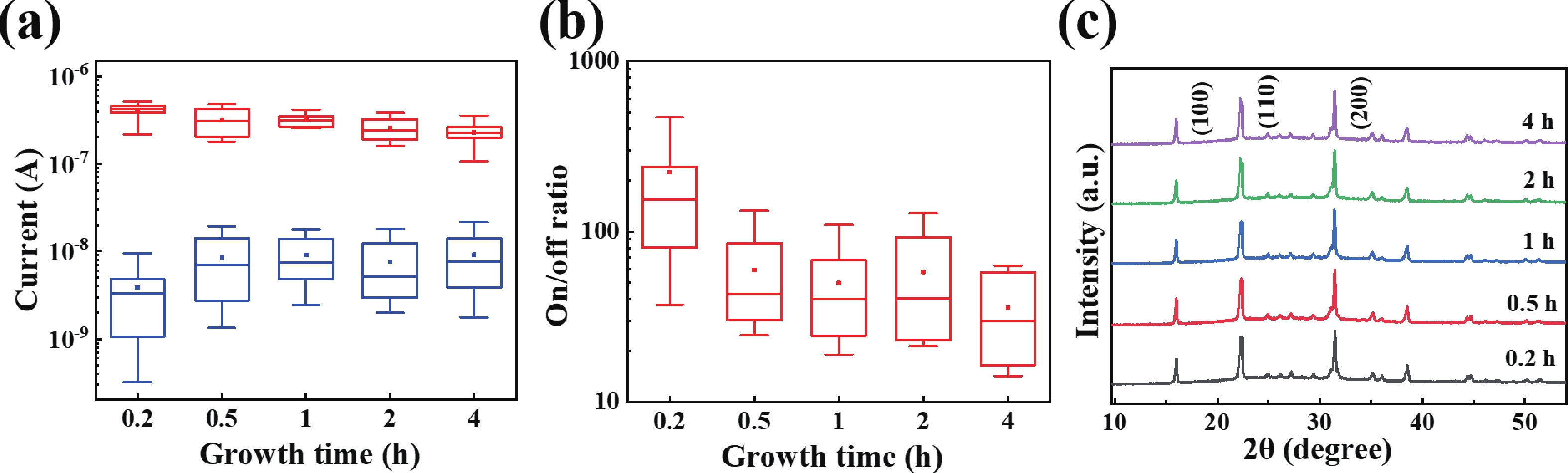
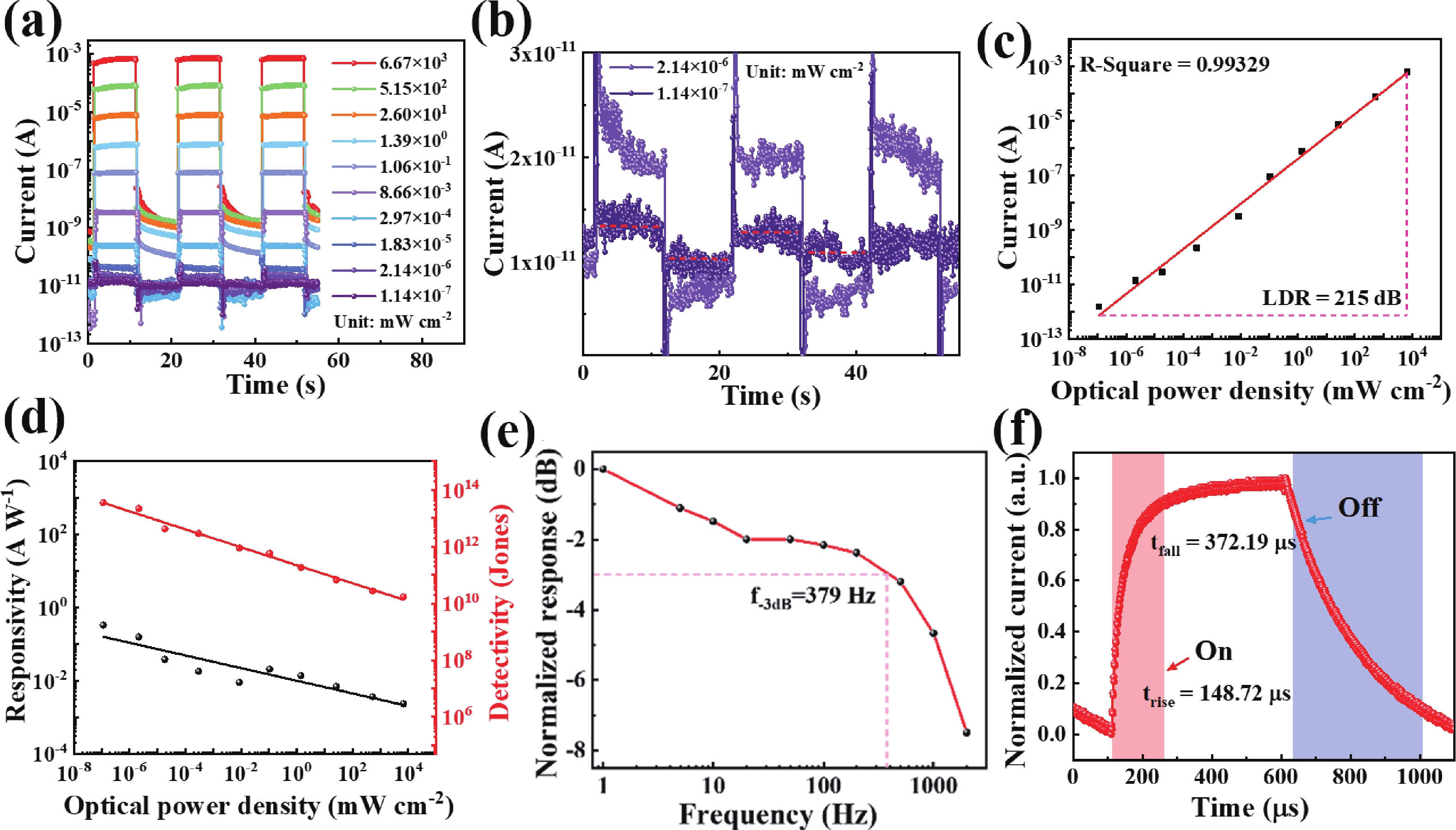
High-performance perovskite photodetectors with self-driven characteristic usually need electron/hole transport layers to extract carriers. However, these devices with transport layer structure are prone to result in a poor perovskite/transport layer interface, which restricts the performance and stability of the device. To solve this problem, this work reports a novel device structure in which perovskite nanowires are in-situ prepared on PbI2, which serves as both a reaction raw material and efficient carrier extraction layer. By optimizing the thickness of PbI2, nanowire growth time, and ion exchange time, a self-driven photodetector with an ITO/PbI2/CsPbBr3/carbon structure is constructed. The optimized device achieves excellent performance with the responsivity of 0.33 A/W, the detectivity of as high as 3.52 × 10¹³ Jones. Furthermore, the device can detect the light with its optical power lowered to 0.1 nW/cm2. This research provides a new method for preparing perovskite nano/micro devices with simple structure but excellent performance.
J. Semicond.
2025, 46(5): 052802 doi: 10.1088/1674-4926/24120026
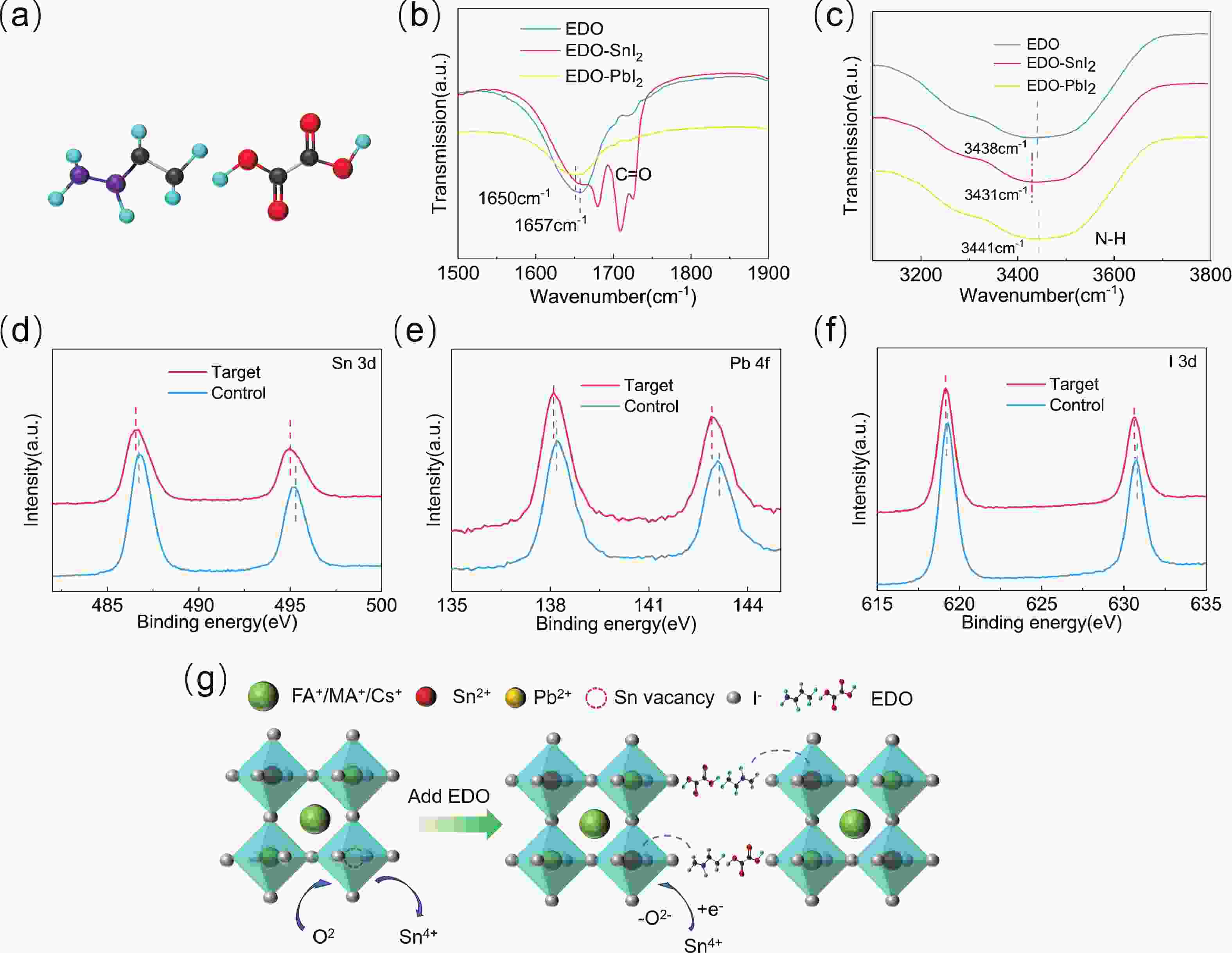
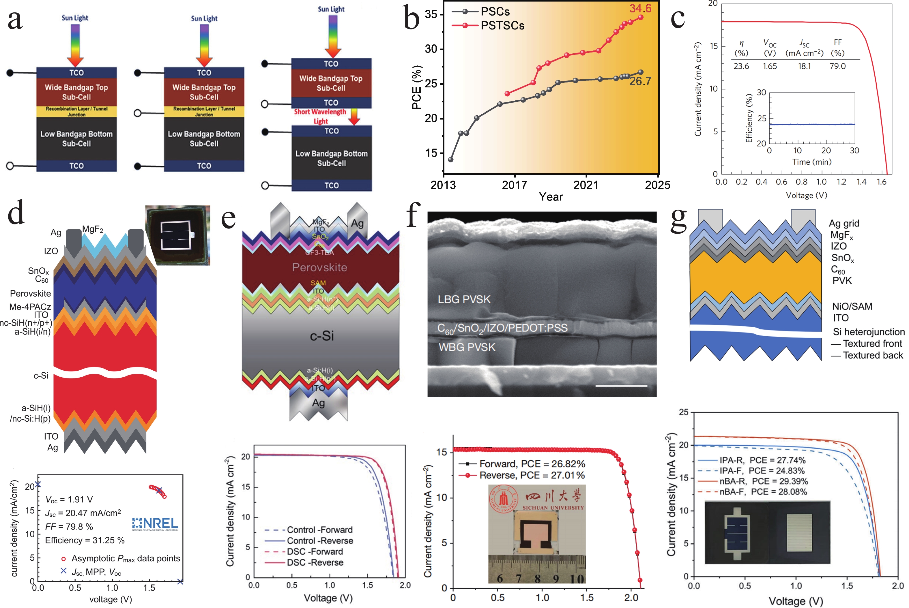
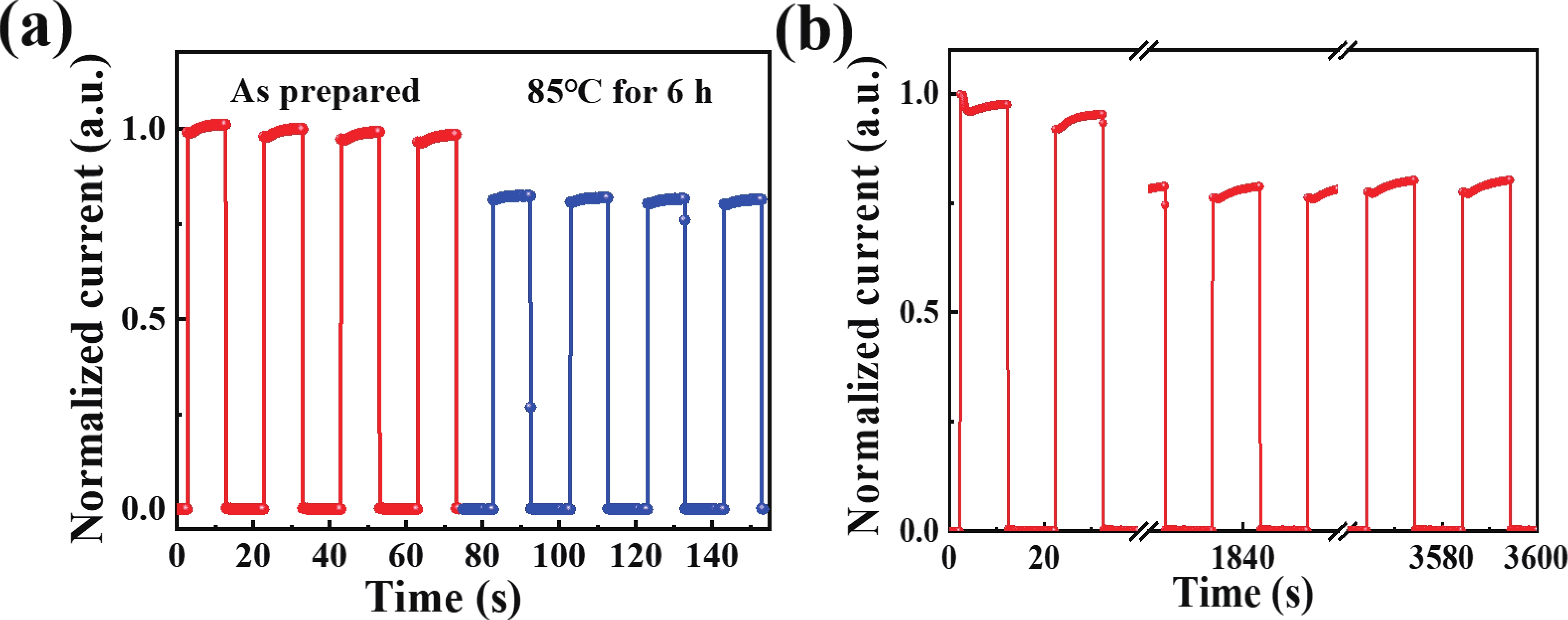
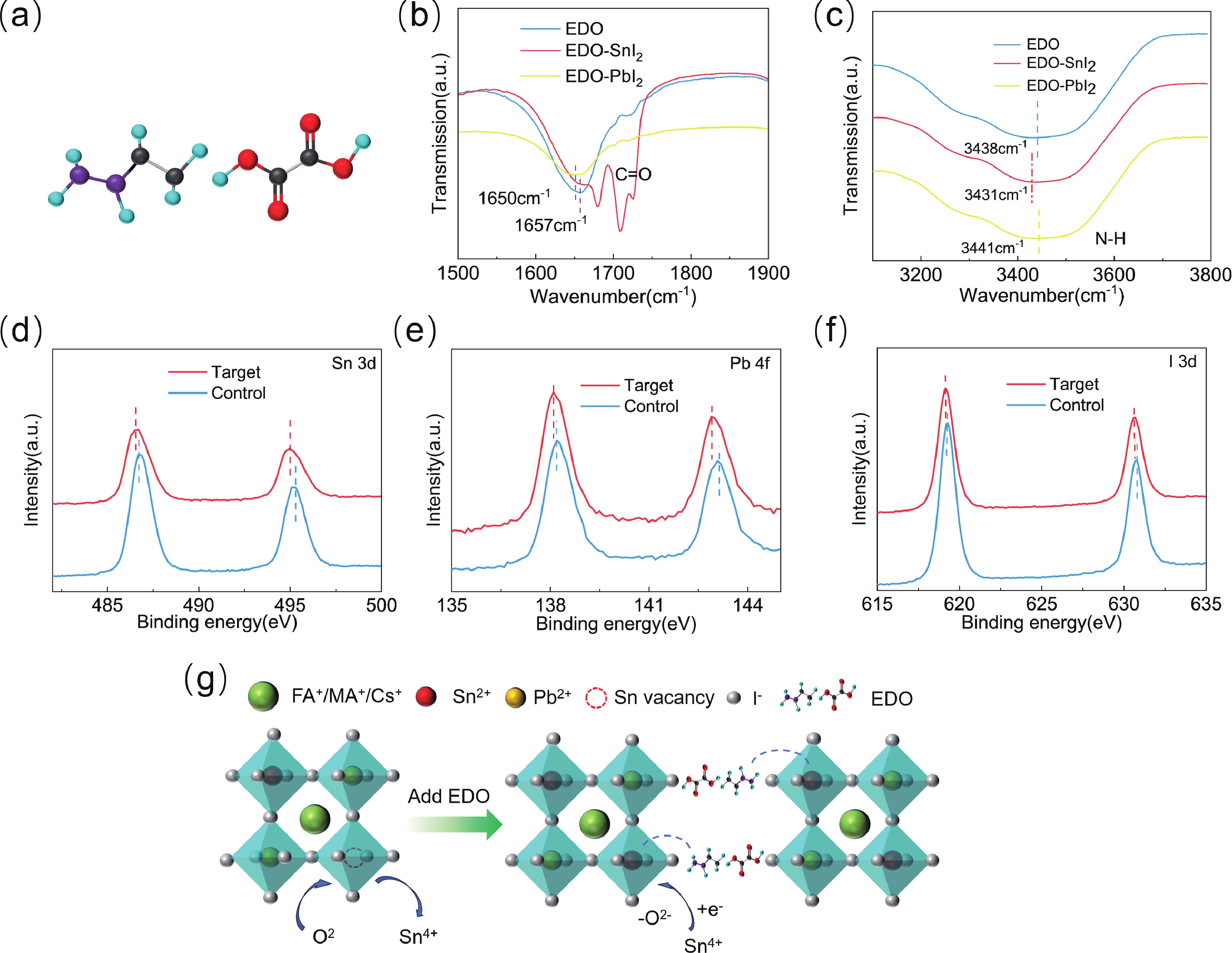
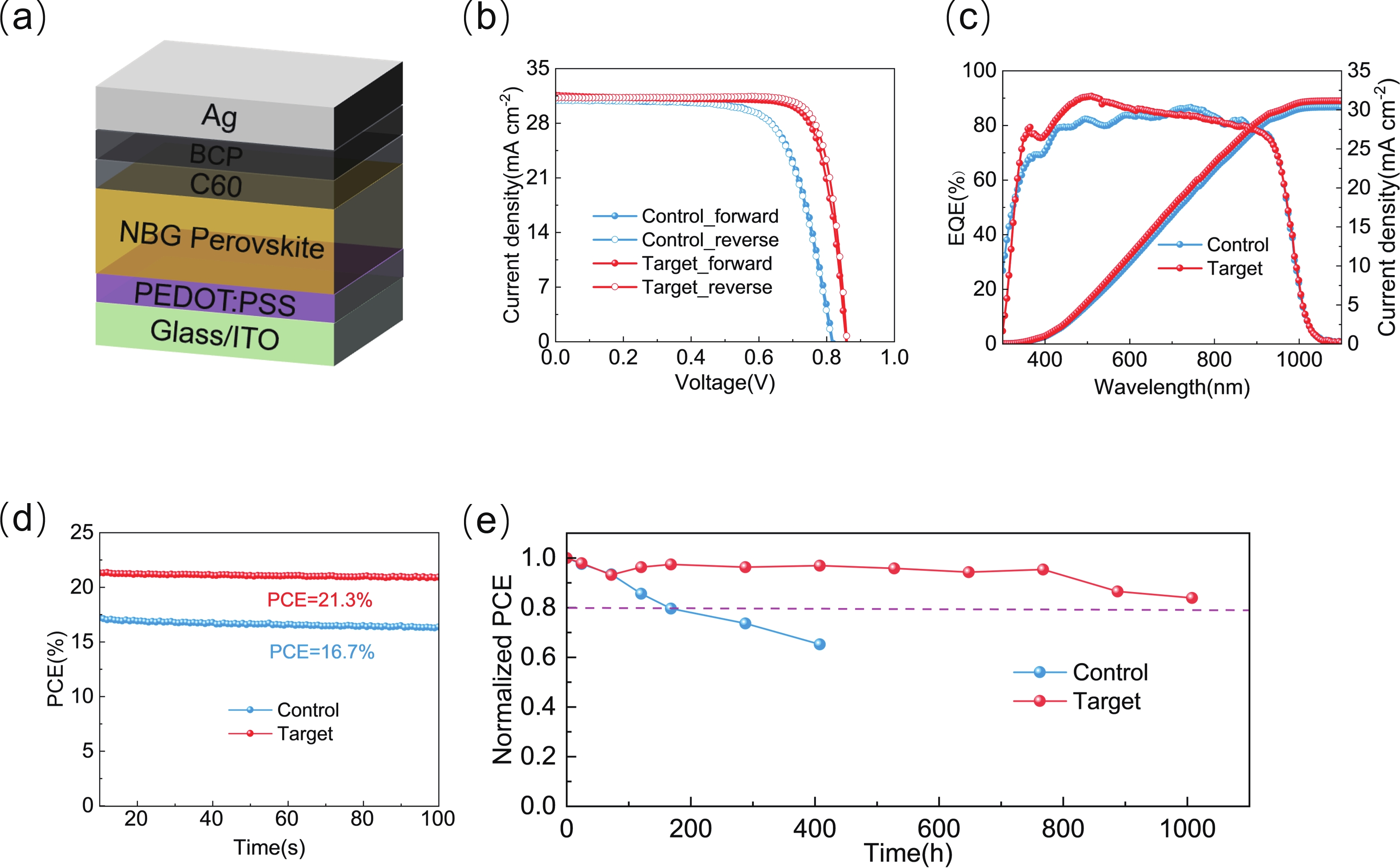
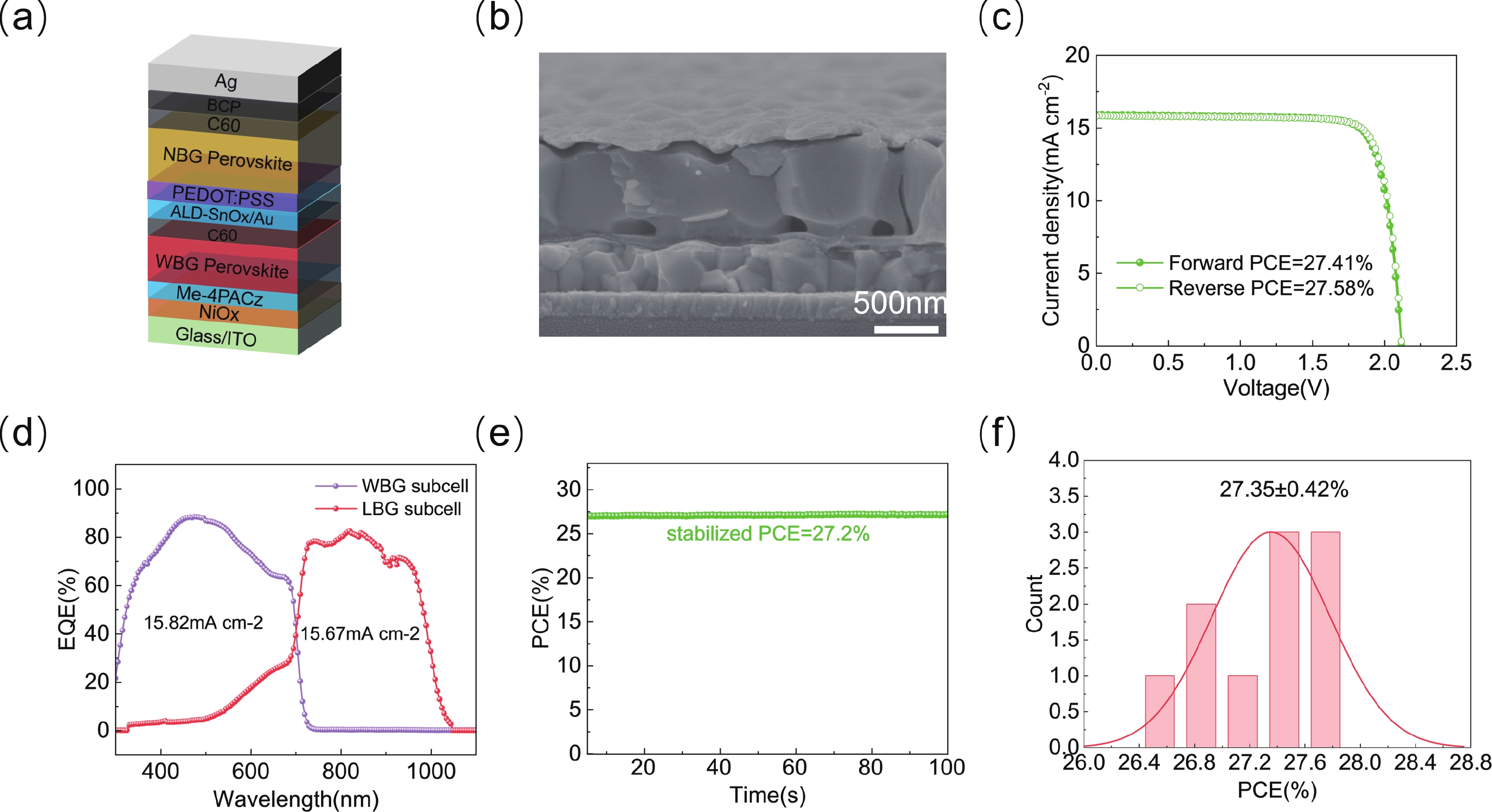
All-perovskite tandem solar cells (ATSCs) have the potential to surpass the Shockley−Queisser efficiency limit of conventional single-junction devices. However, the performance and stability of mixed tin–lead (Sn–Pb) perovskite solar cells (PSCs), which are crucial components of ATSCs, are much lower than those of lead-based perovskites. The primary challenges include the high crystallization rate of perovskite materials and the susceptibility of Sn2+ oxidation, which leads to rough morphology and unfavorable p-type self-doping. To address these issues, we introduced ethylhydrazine oxalate (EDO) at the perovskite interface, which effectively inhibits the oxidation of Sn2+ and simultaneously enhances the crystallinity of the perovskite. Consequently, the EDO-modified mixed tin−lead PSCs reached a power conversion efficiency (PCE) of 21.96% with high reproducibility. We further achieved a 27.58% efficient ATSCs by using EDO as interfacial passivator in the Sn−Pb PSCs.

J. Semicond.
2025, 46(5): 052803 doi: 10.1088/1674-4926/24120038
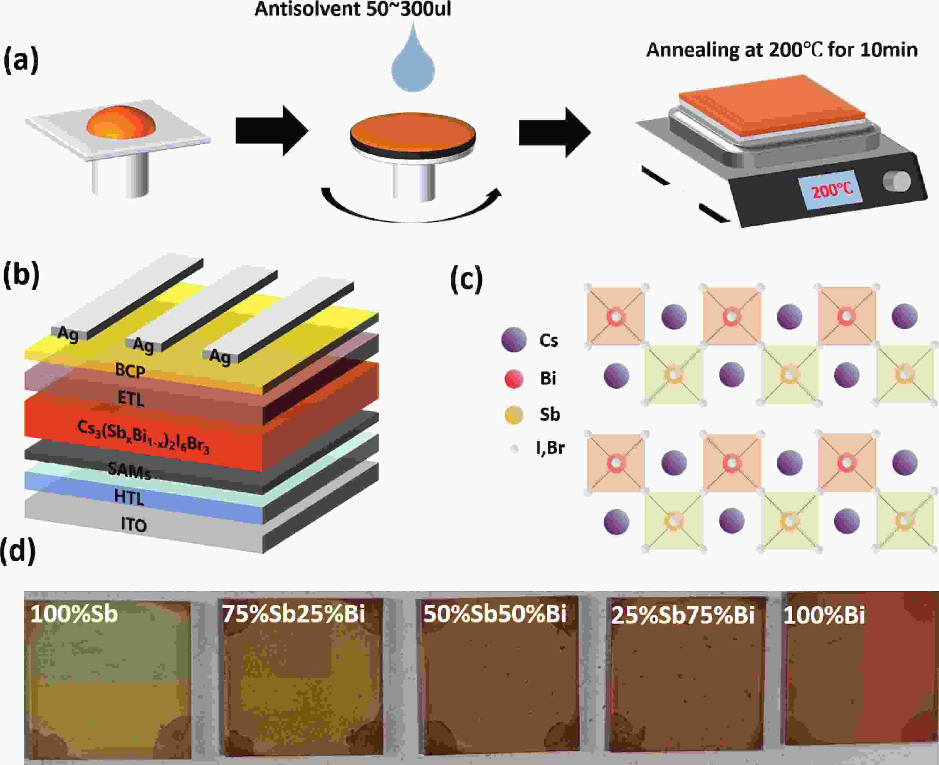
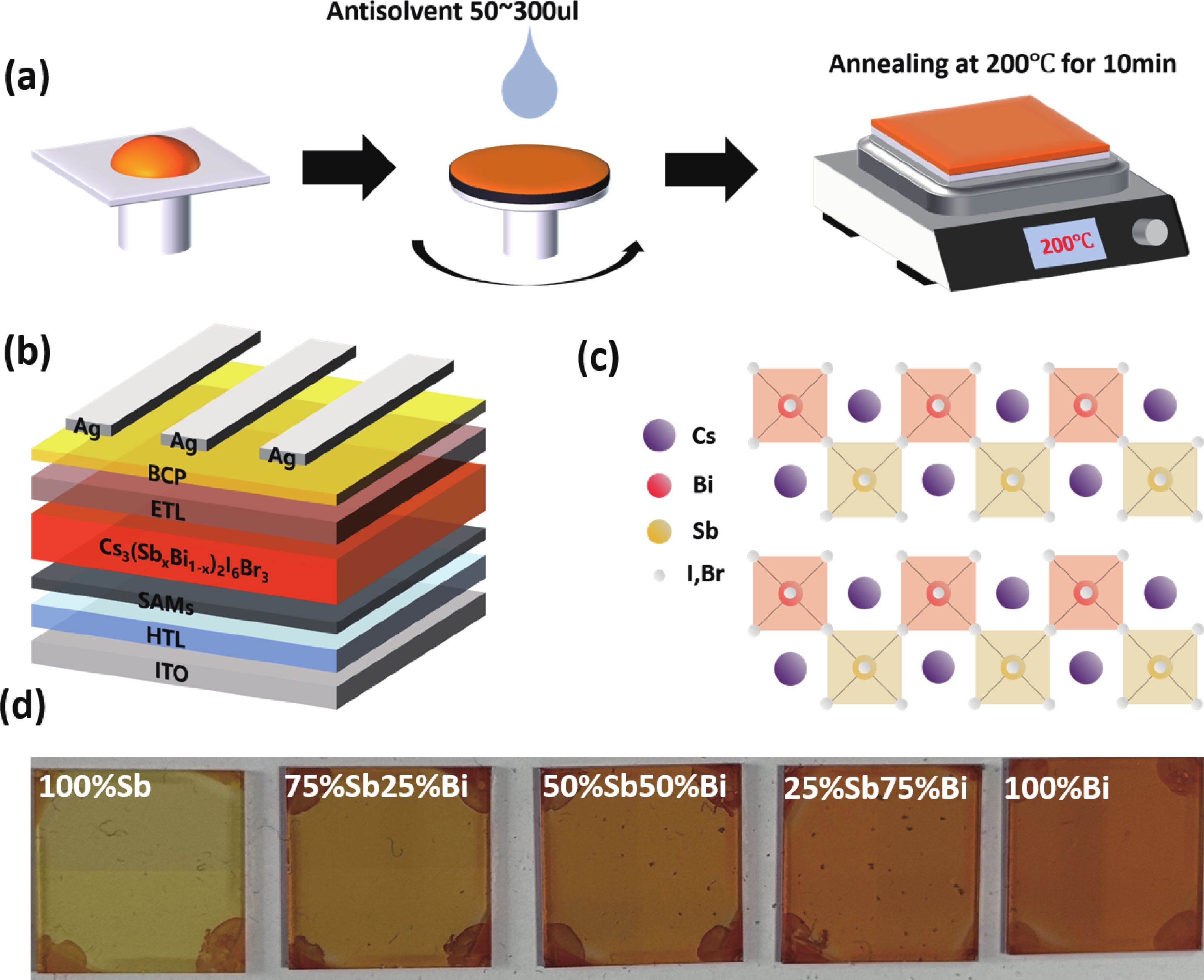
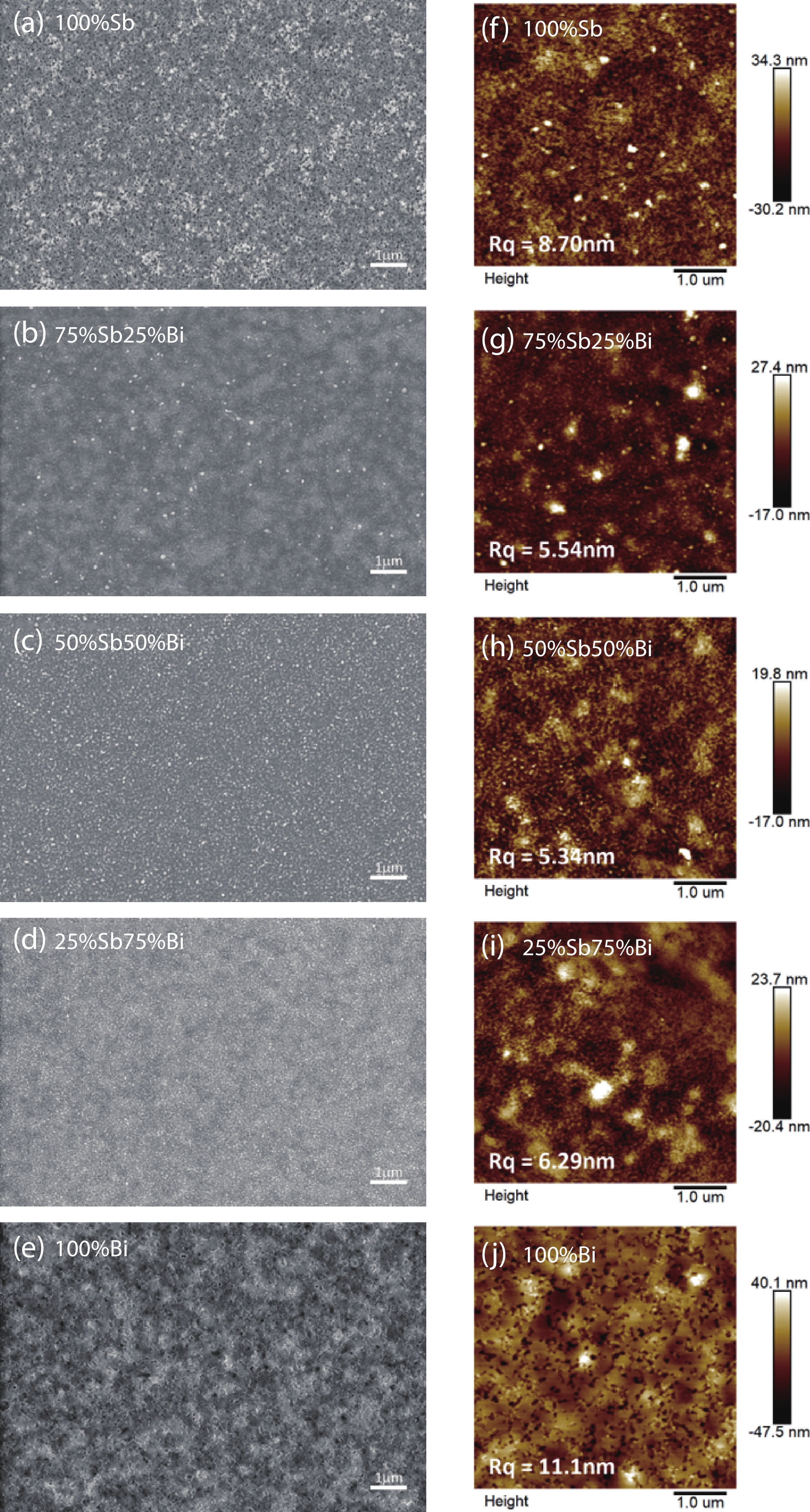
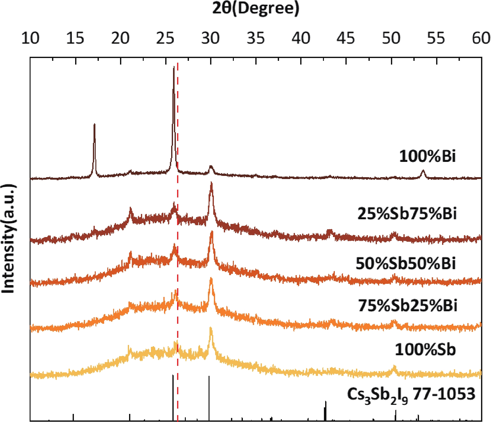
Owing to their low toxicity and remarkable stability, perovskites based on antimony and bismuth have garnered significant interest in recent years. However, A3B2X9 perovskite materials derived from antimony and bismuth face several challenges, including excessively wide band gaps, elevated defect densities, and suboptimal film quality, all of which hinder advancements in device efficiency. While extensive studies have been undertaken to investigate the effects of modulating the A-site and X-site elements in lead-free A3B2X9 perovskites, there remains a notable scarcity of reports addressing the impact of modifications to the B-site element. In this study, we investigated the alloying of antimony and bismuth within the 2D Cs3B2I6Br3 perovskite. By systematically varying the ratios of two elements, we found that the incorporation of both antimony and bismuth at the B-site significantly enhances the quality of the perovskite films. Our findings indicate that a 1 : 1 ratio of antimony to bismuth produces the densest films, the highest photoluminescence intensity, and superior photovoltaic performance. Ultimately, the devices fabricated using this optimal ratio achieved an open-circuit voltage (VOC) of 1.01 V and a power conversion efficiency (PCE) of 0.645%.

J. Semicond.
2025, 46(5): 052804 doi: 10.1088/1674-4926/25030040
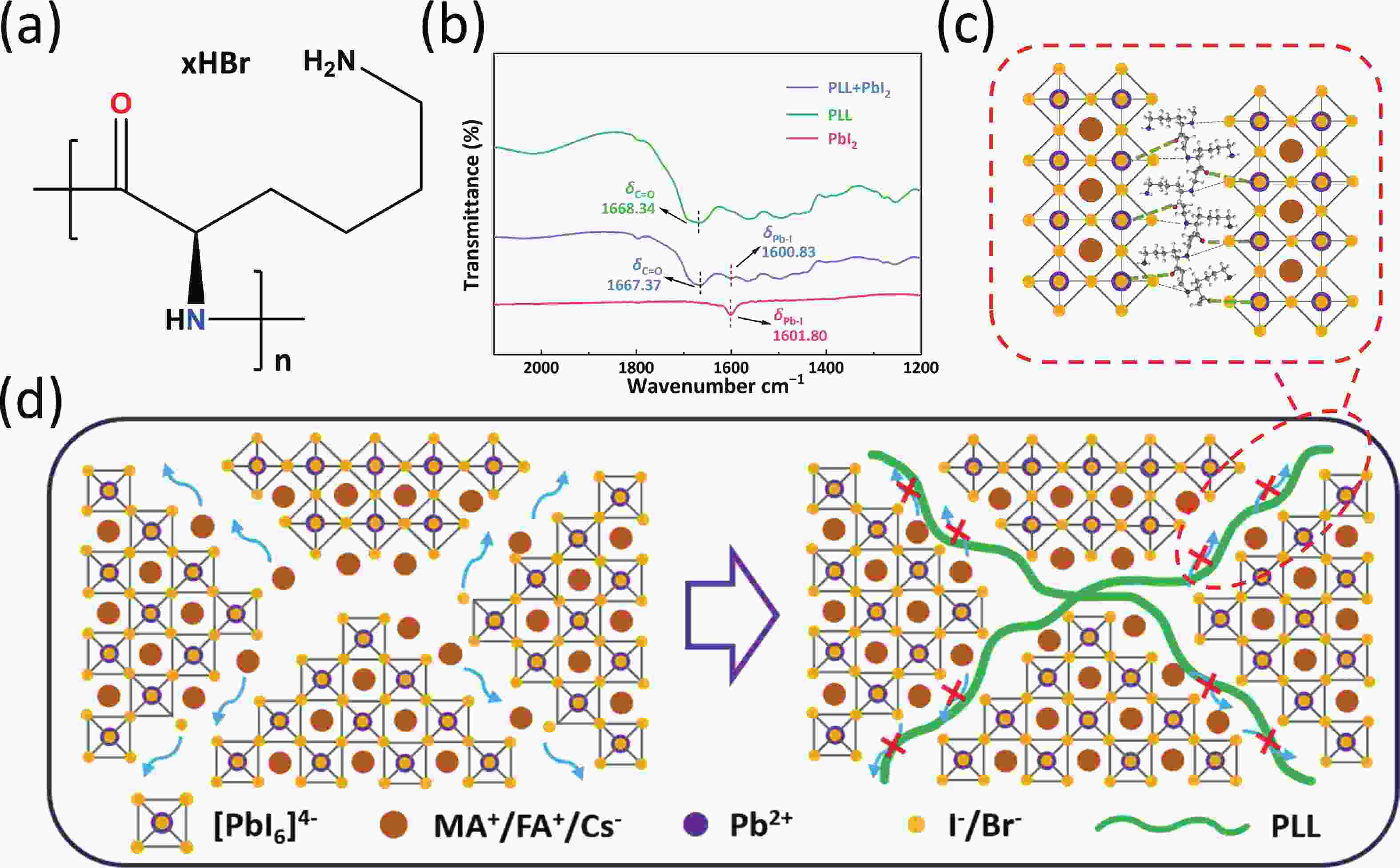
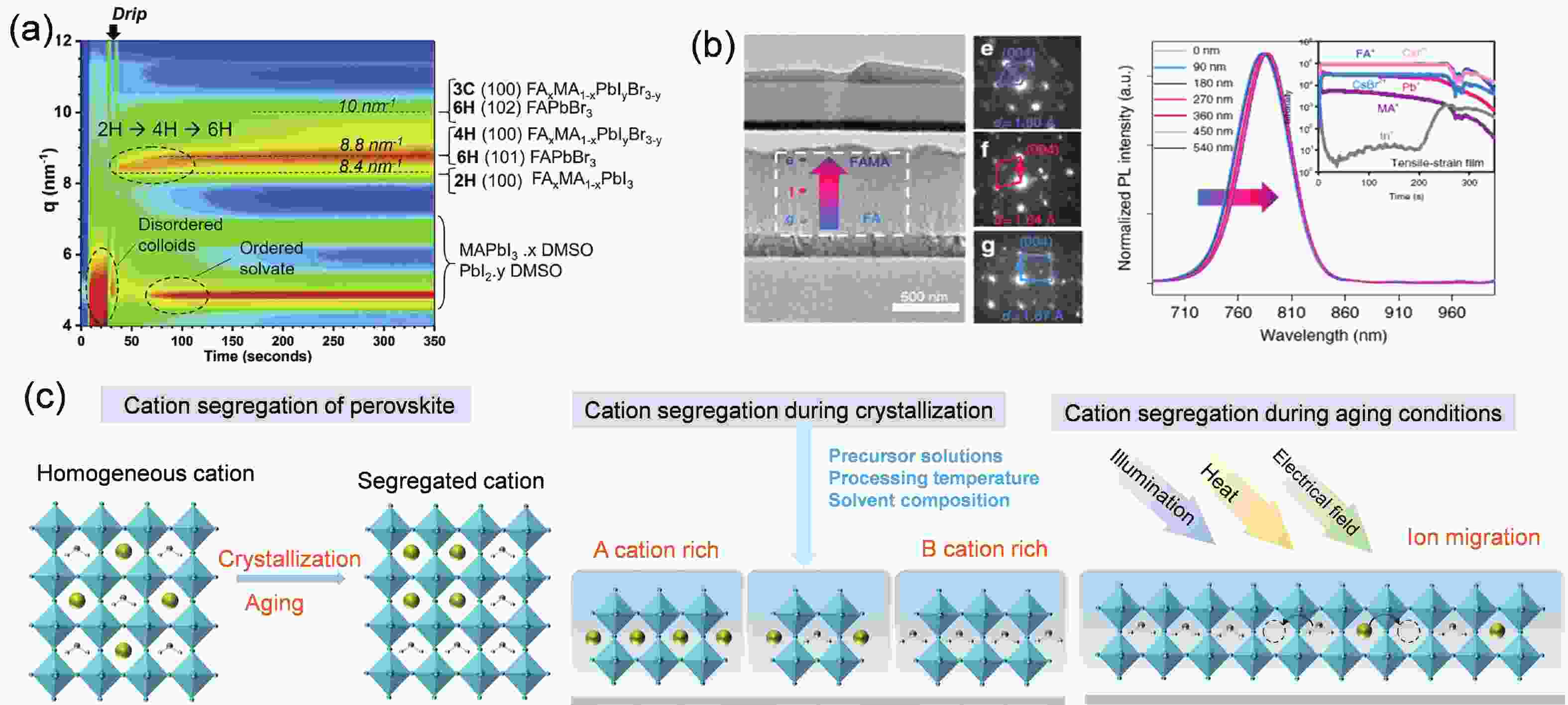
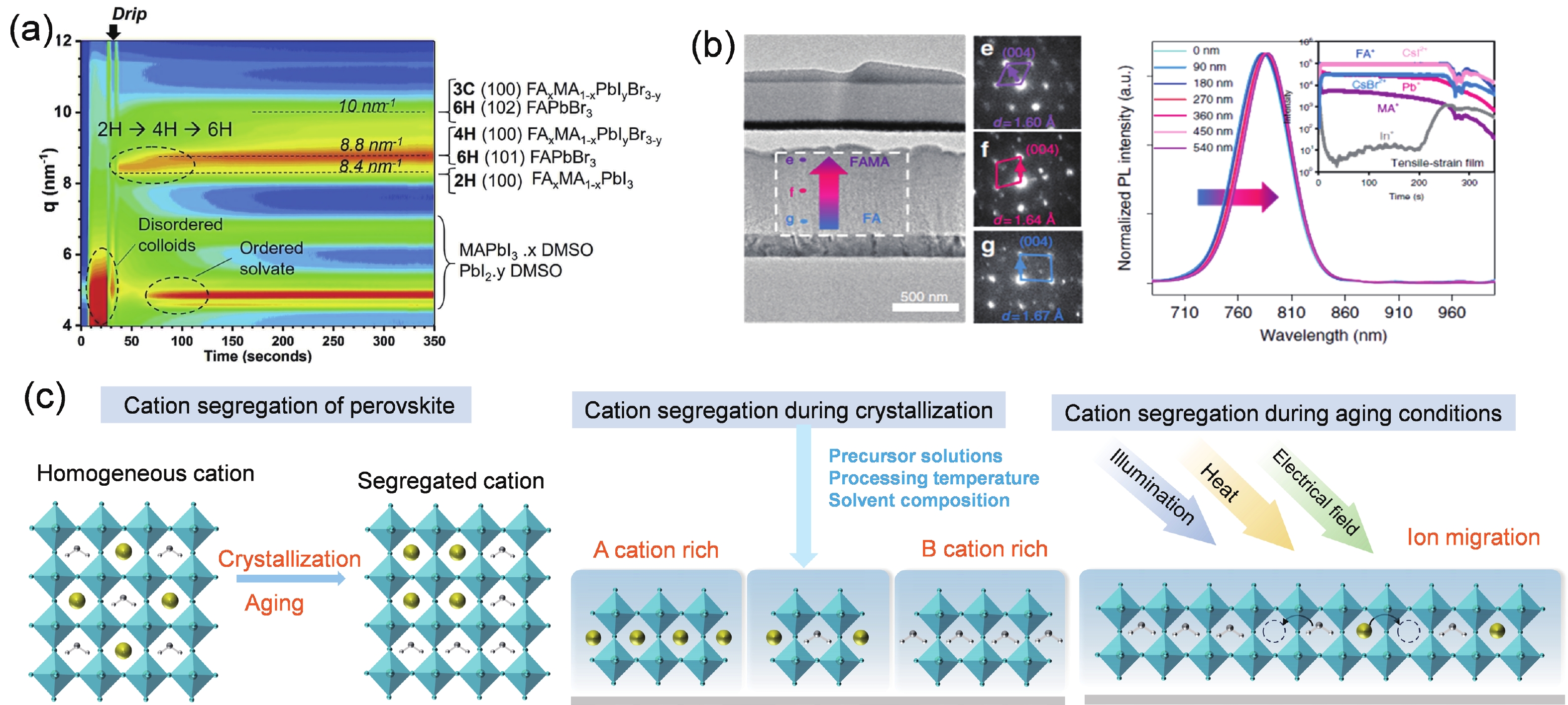
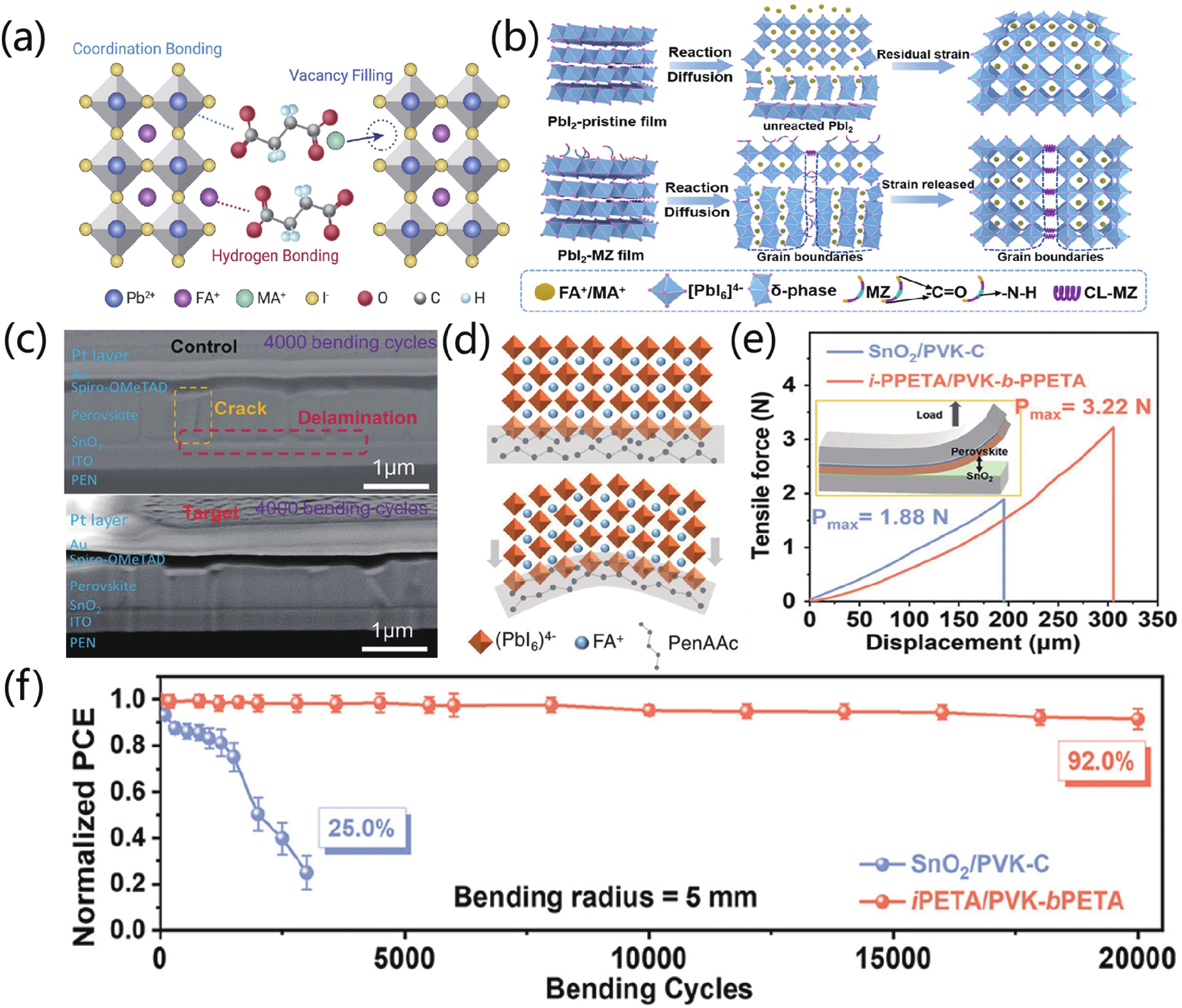
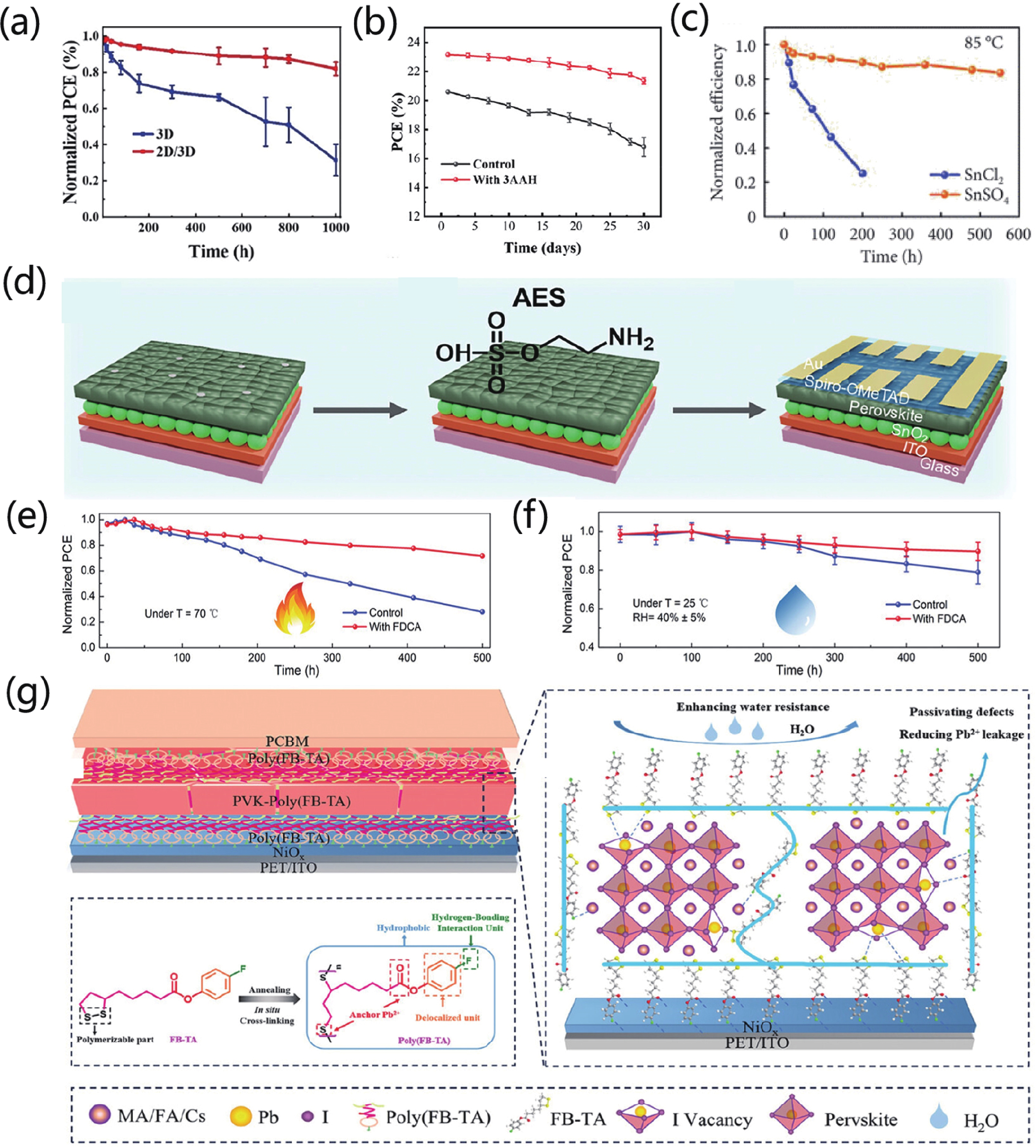
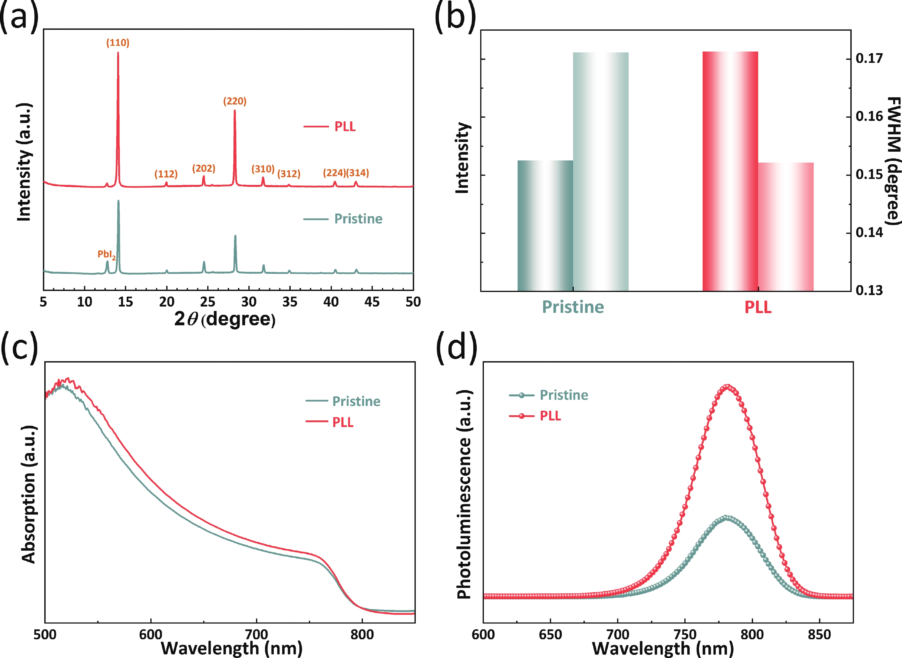
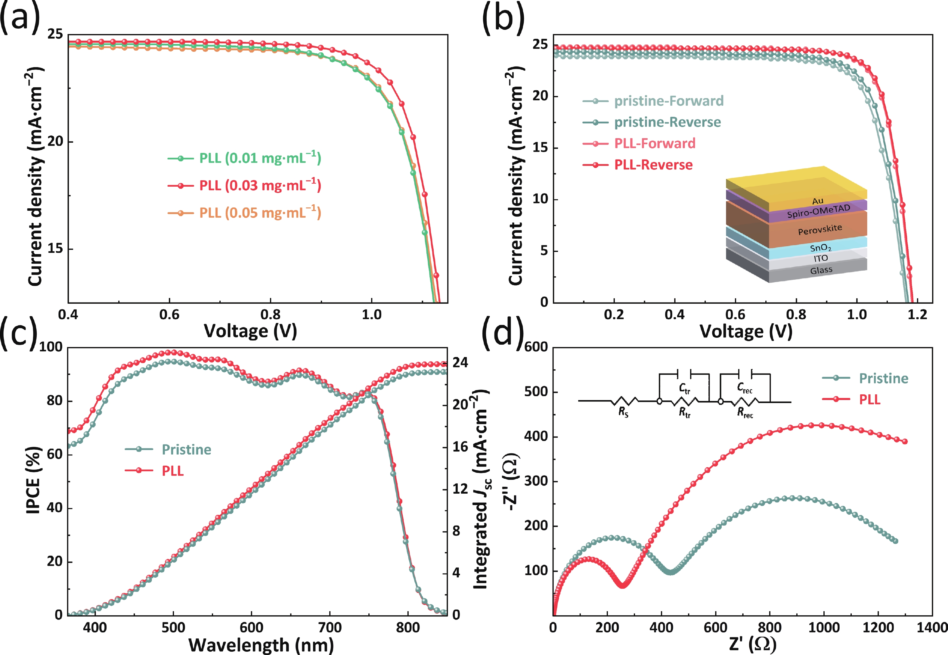
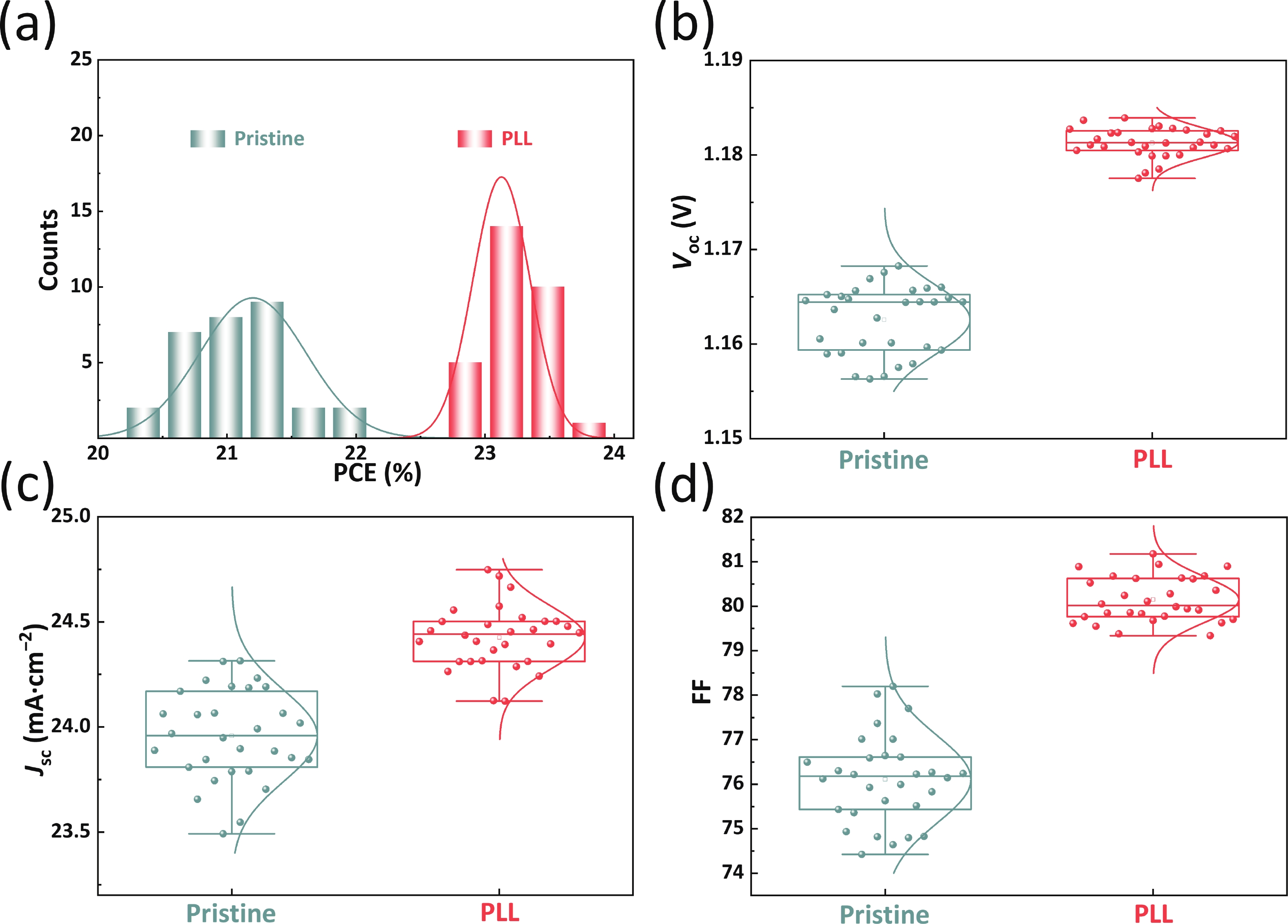
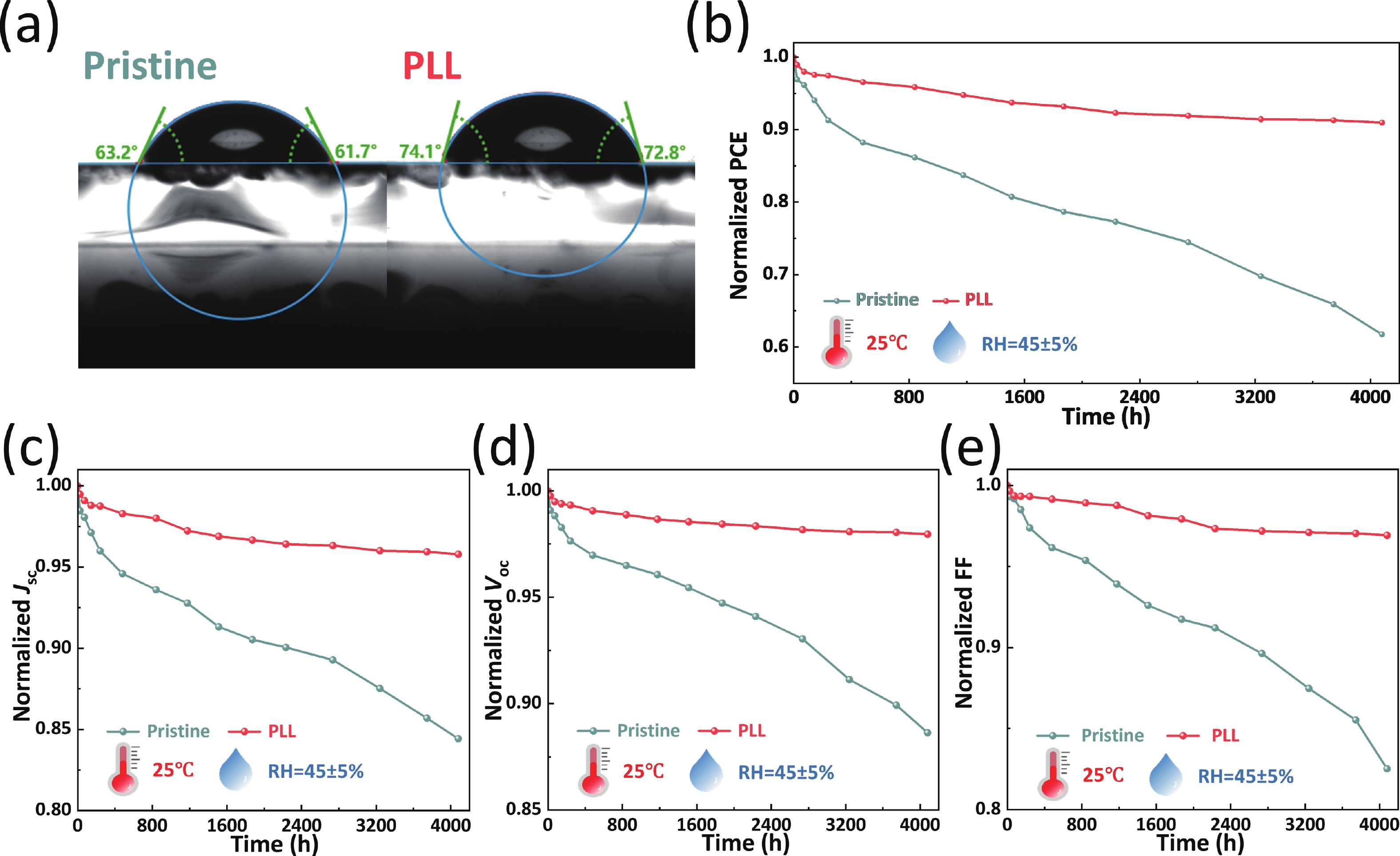
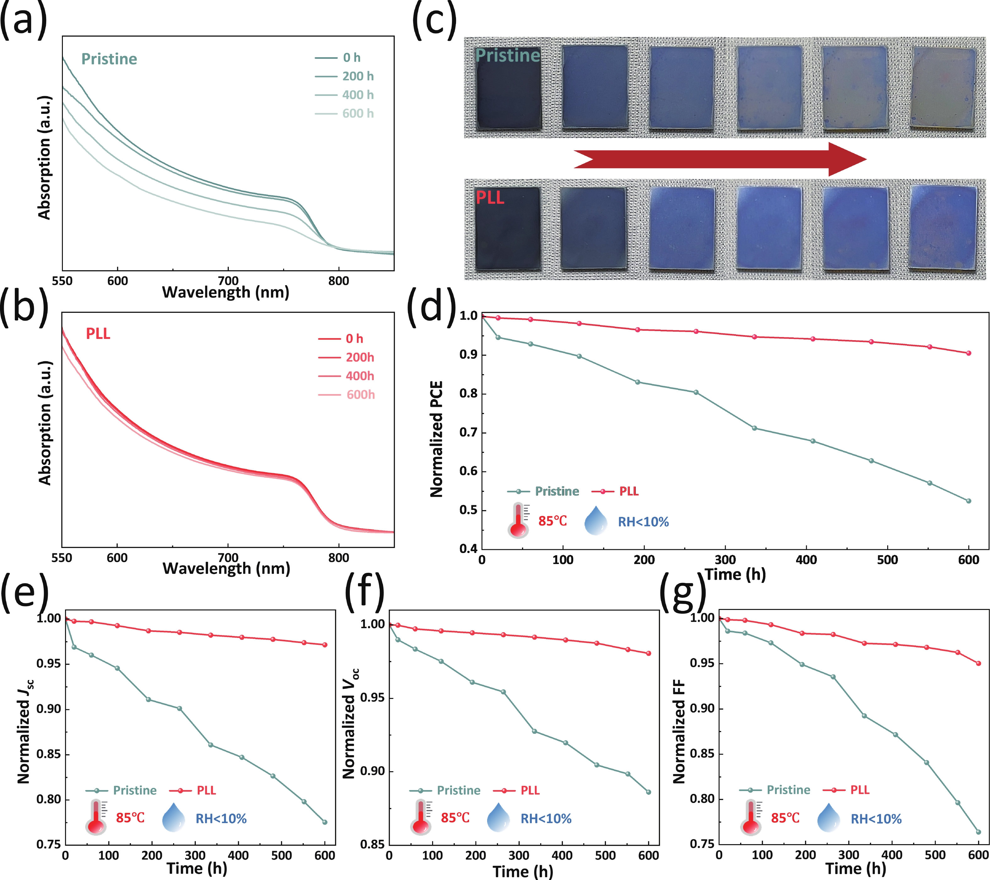
Although perovskite solar cells (PSCs) demonstrate outstanding power conversion efficiency (PCE), their practical applications are still limited by stability issues caused by various problems such as poor crystal quality triggered structural instability. Herein, to address the structural instability of perovskites, we introduced a polymer additive, poly-L-lysine hydrobromide (PLL), into the perovskite precursor to promote perovskite crystal growth, thereby constructing a stable crystal structure. The results show that the introduction of PLL modulates the colloidal aggregation state in the precursor solution, provides longer time for growth of perovskite and successfully realizes the formation of large-sized perovskite films with high crystallinity. More importantly, owing to its hydrophobic long-chain structure and the widespread distribution of C=O and NH on the chain, PLL firmly locks the perovskite crystals, enhancing their structural stability while blocking the intrusion of external factors such as water molecules, significantly enhances the overall stability of the device. The results show that the PLL-based PSC has negligible hysteresis and its PCE is improved from 22.20% to 23.66%. while the PLL-modified perovskite films and devices demonstrate excellent thermal and environmental stability. These findings highlight PLL as a promising additive for optimizing perovskite crystallization, offering guidance for fabricating efficient and stable photovoltaic devices.

J. Semicond.
2025, 46(5): 052805 doi: 10.1088/1674-4926/25030046

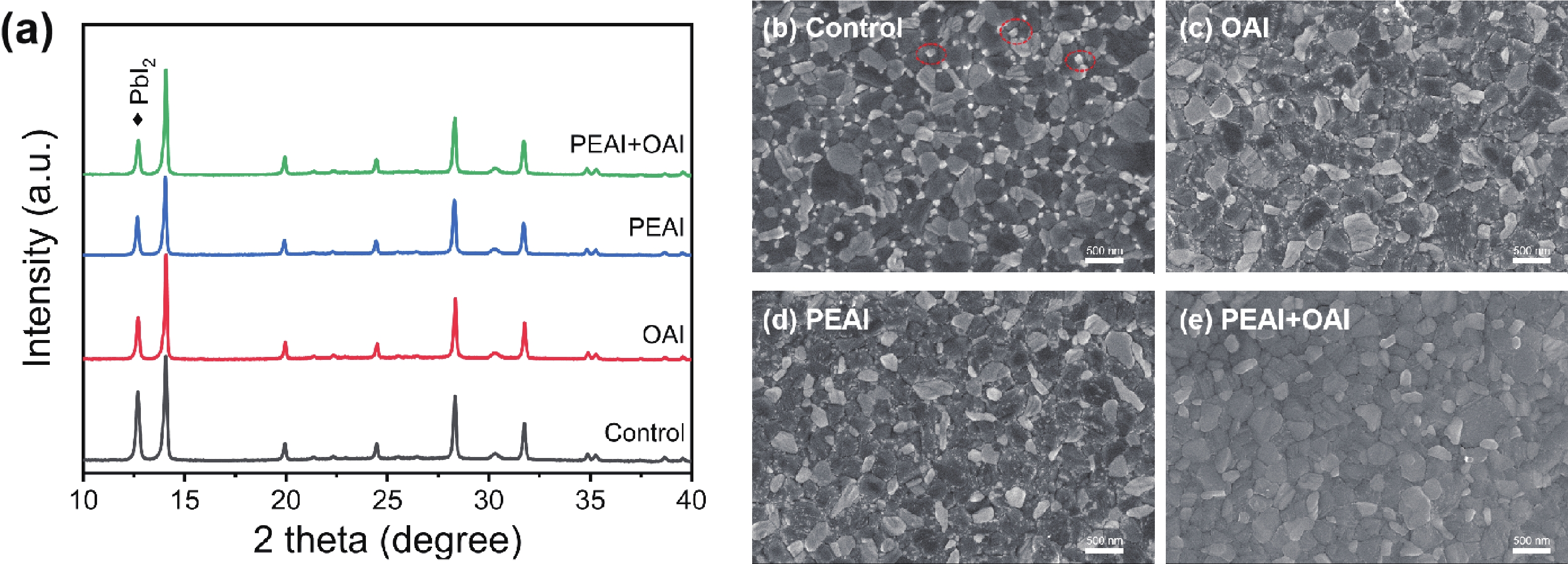
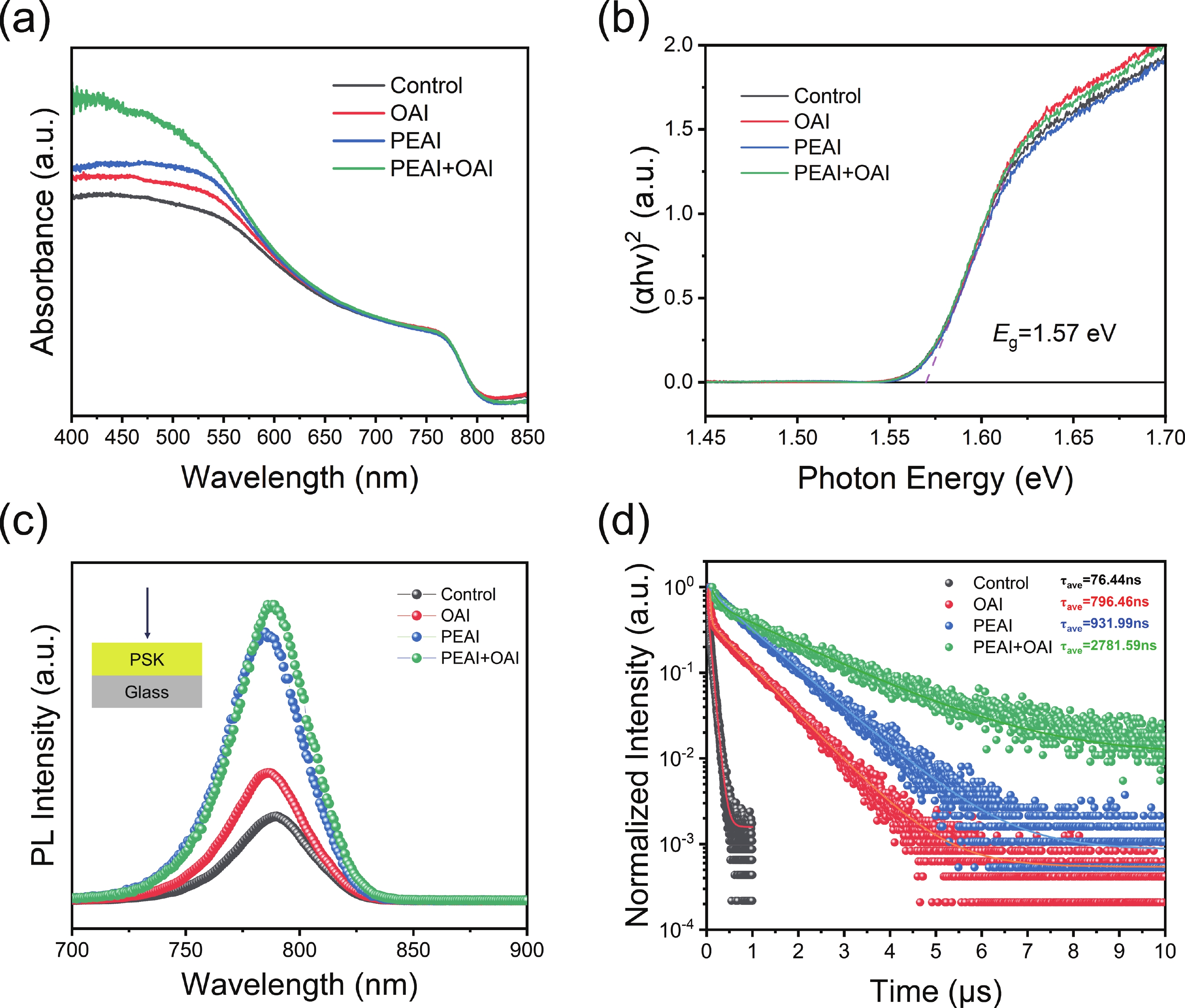
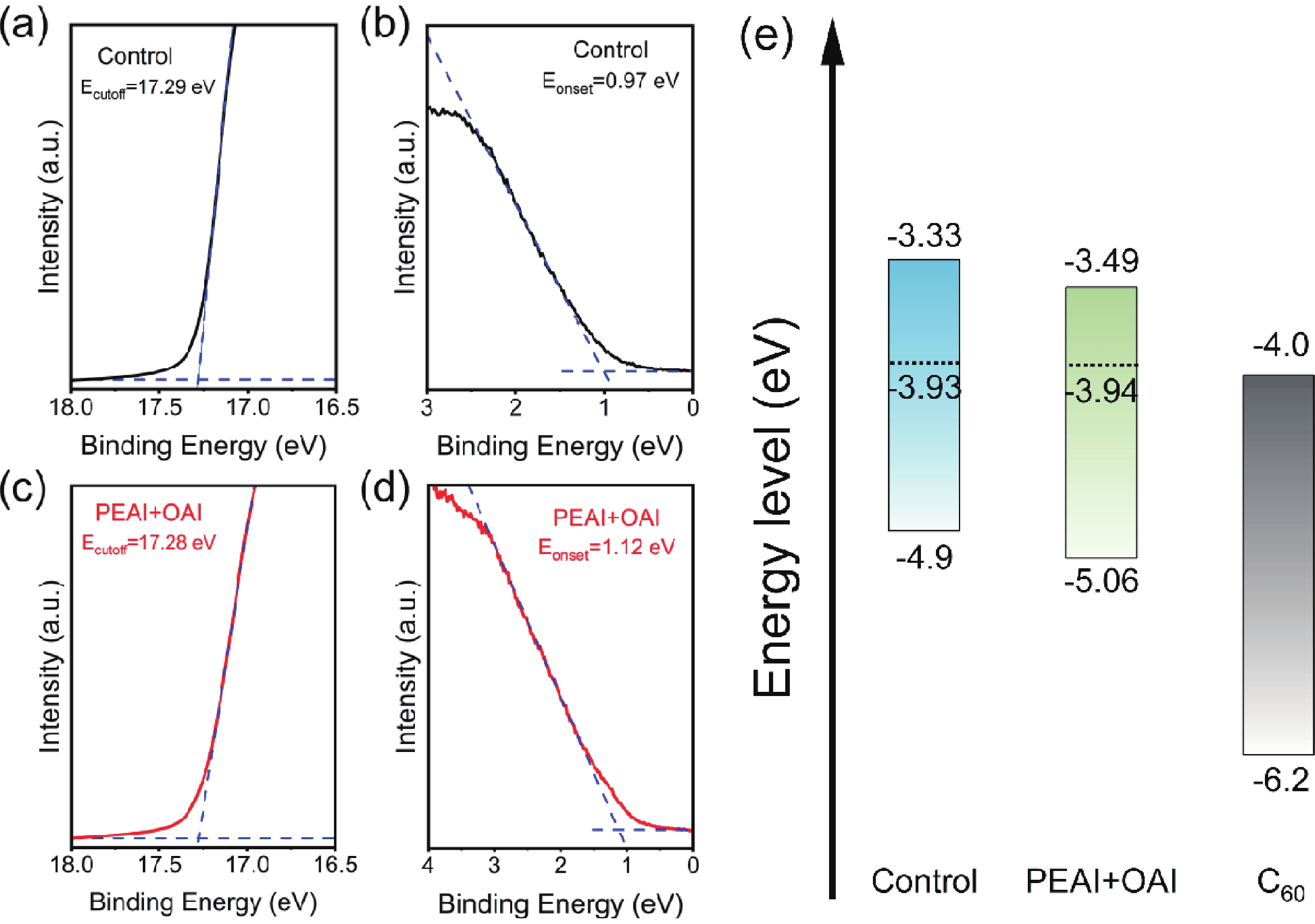
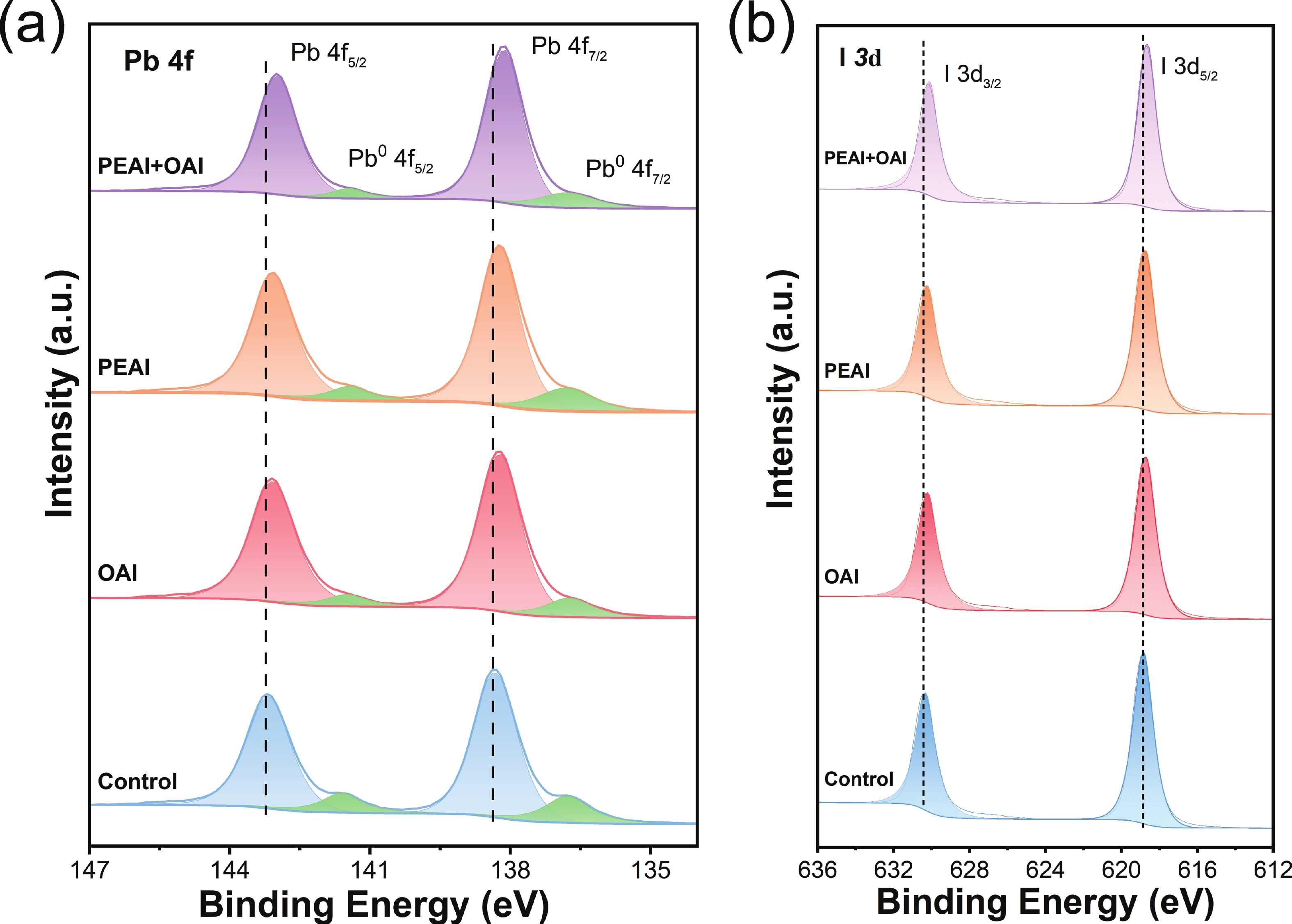
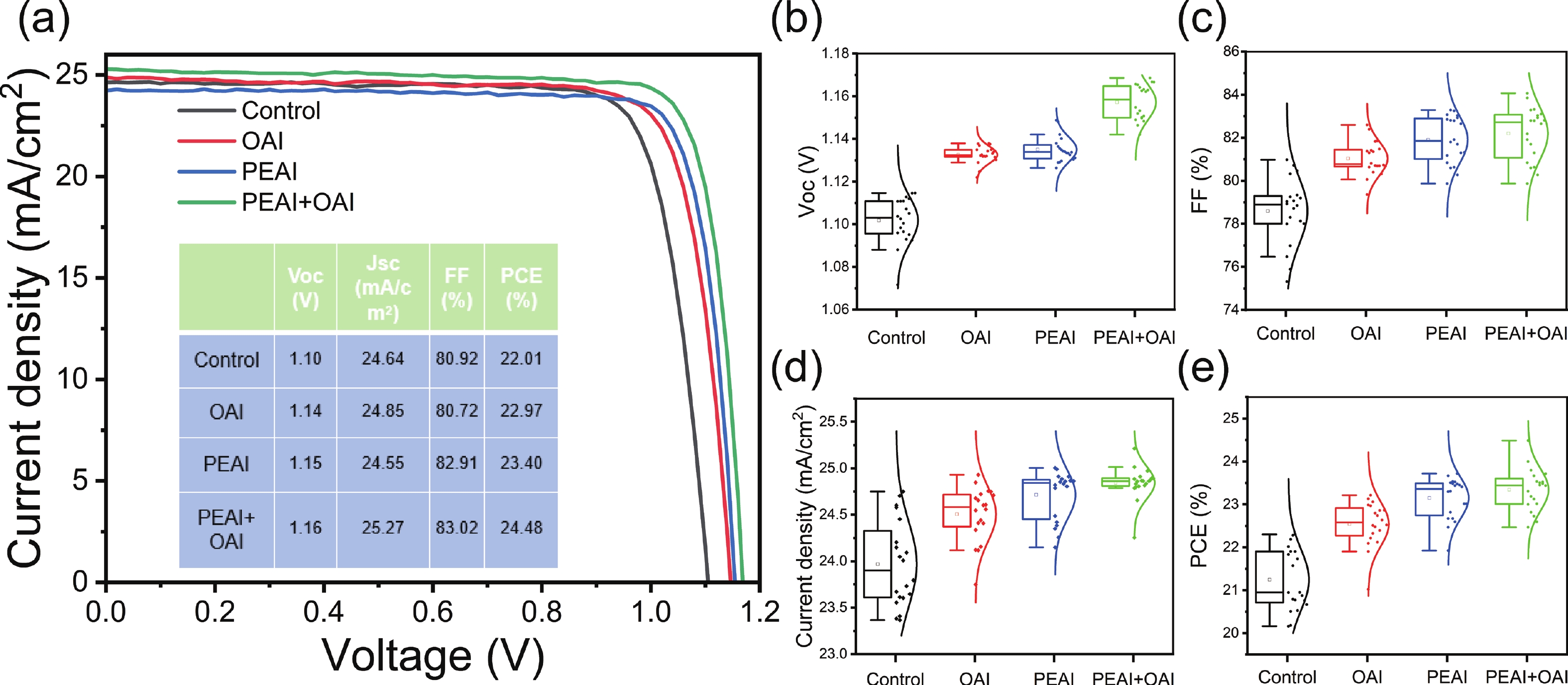
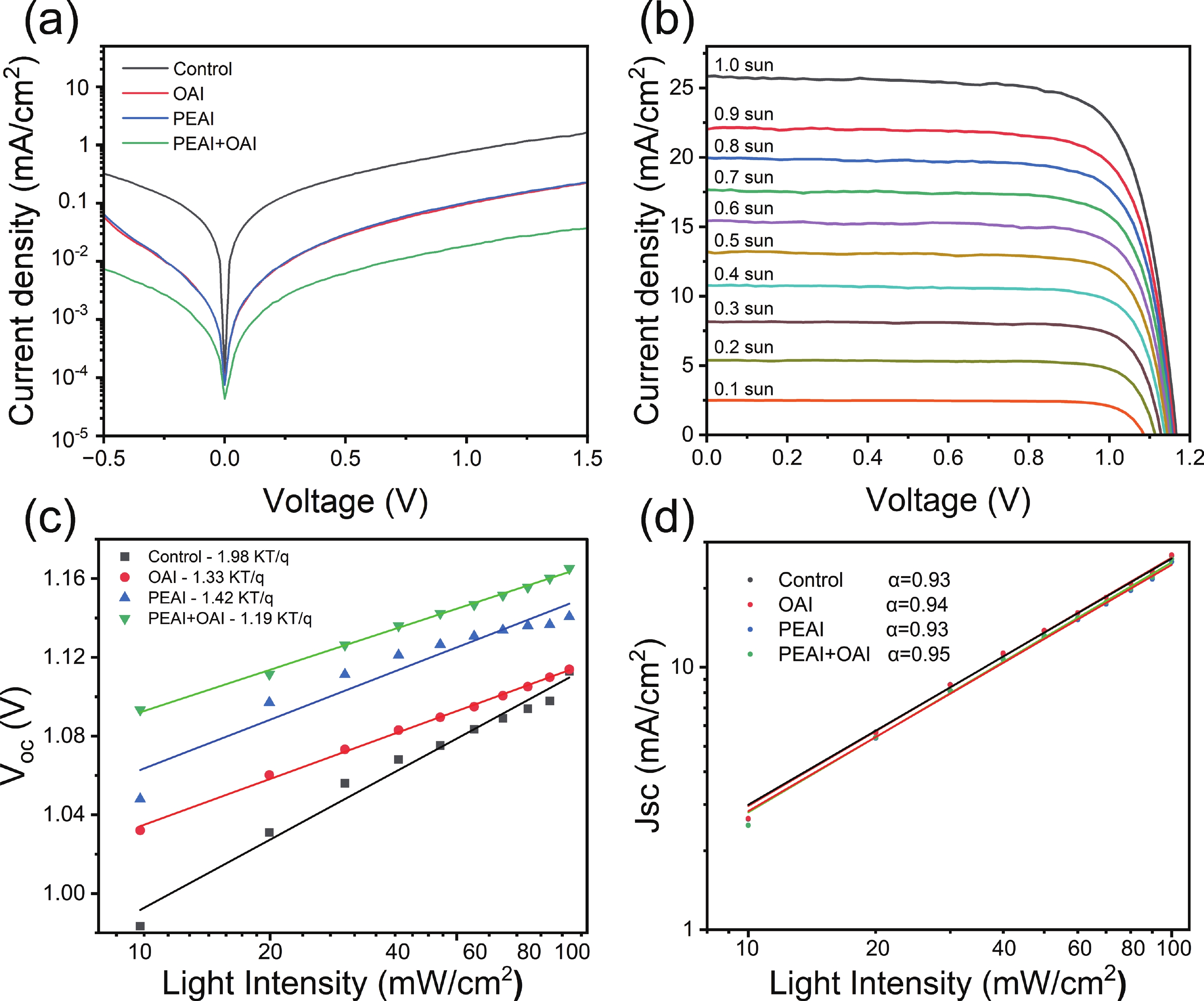
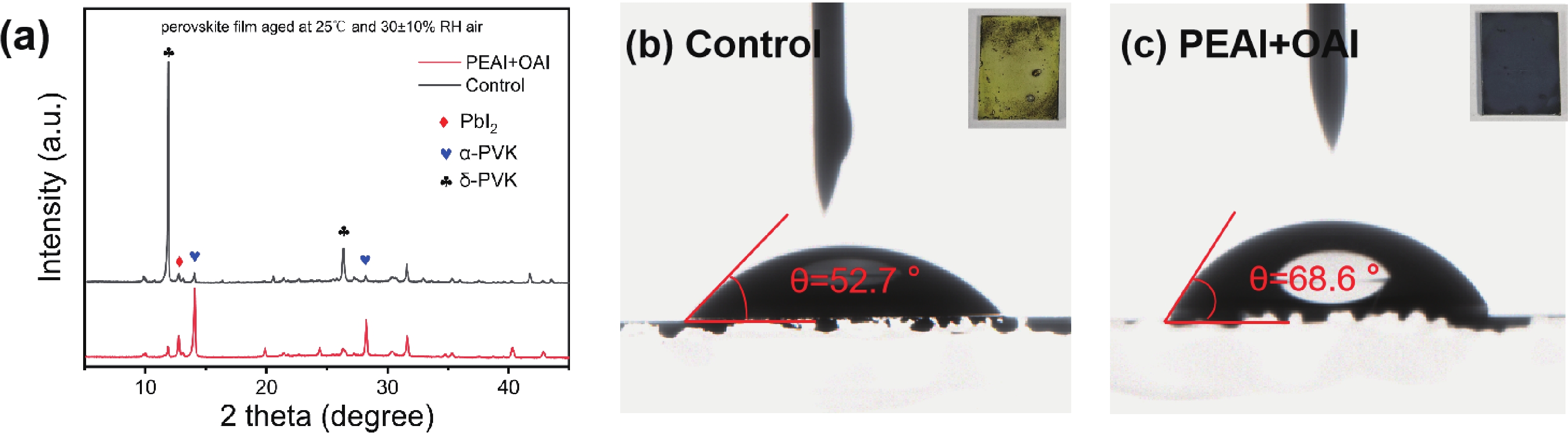
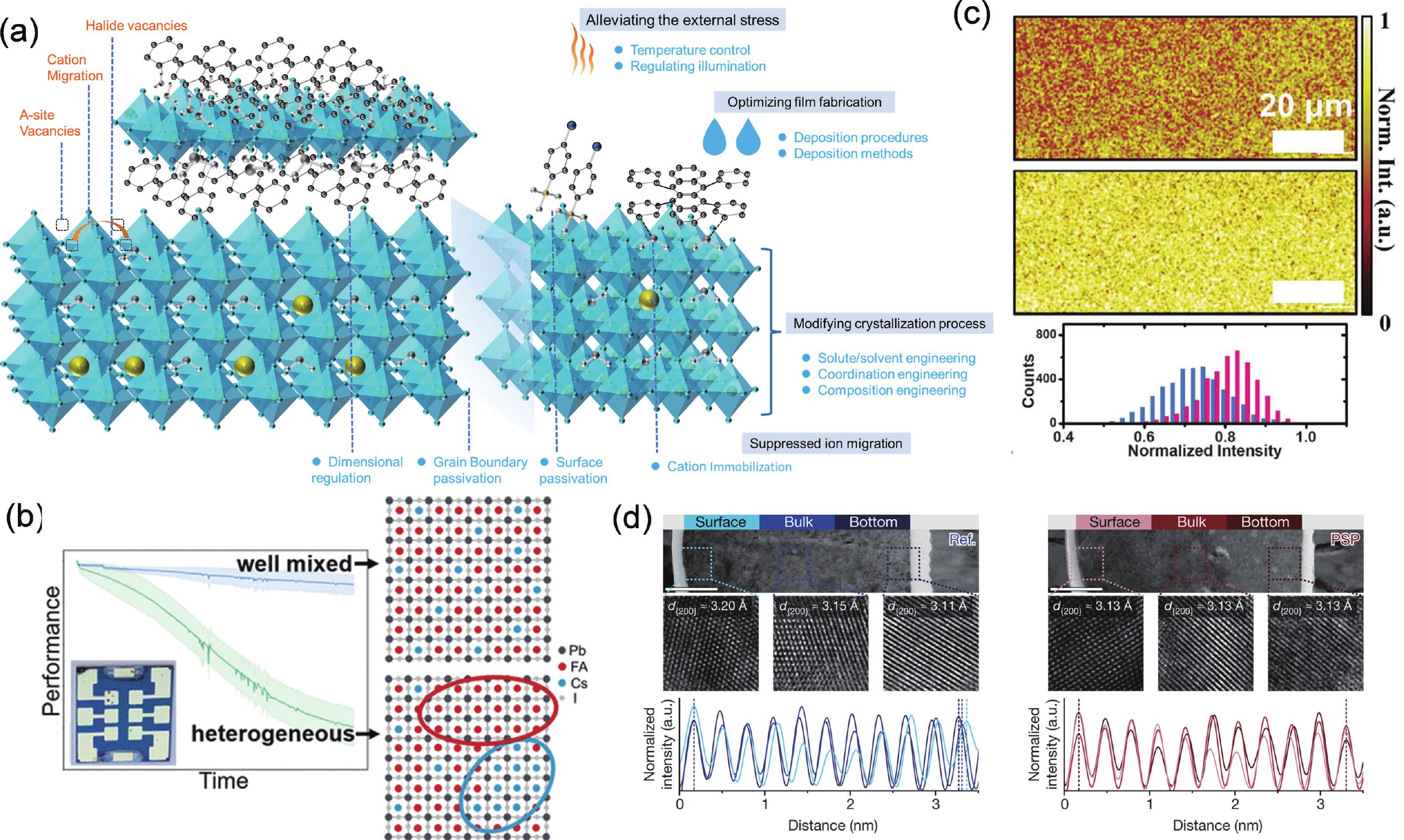
Interfacial defects and environmental instability at perovskite surfaces pose significant challenges for inverted perovskite solar cells (PSCs). Surface post-treatment strategies have emerged as a viable approach to improve film quality and passivate defects. Although organic molecules can passivate both surfaces and grain boundaries via hydrogen or covalent bonding, their limited adsorption specificity often results in incomplete defect neutralization. In this work, we introduce a bilayer passivation approach employing phenethylammonium iodide (PEAI) and n-octylammonium iodide (OAI) to concurrently mitigate non-radiative recombination and improve stability. PEAI passivates undercoordinated Pb2+ at grain boundaries and surfaces, effectively eliminating deep-level traps and suppressing non-radiative losses. Meanwhile, OAI forms a hydrophobic barrier on the perovskite surface through its long alkyl chains, inhibiting moisture penetration without compromising interfacial charge transport. As a result, the perovskite film exhibits significantly enhanced optoelectronic performance and environmental stability, achieving a champion power conversion efficiency (PCE) of 24.48%.