Issue Browser
Volume 46, Issue 7,
Jul 2025
Column

Review on three-dimensional graphene: synthesis and joint photoelectric regulation in photodetectors
J. Semicond.
2025, 46(7): 071401 doi: 10.1088/1674-4926/25010015

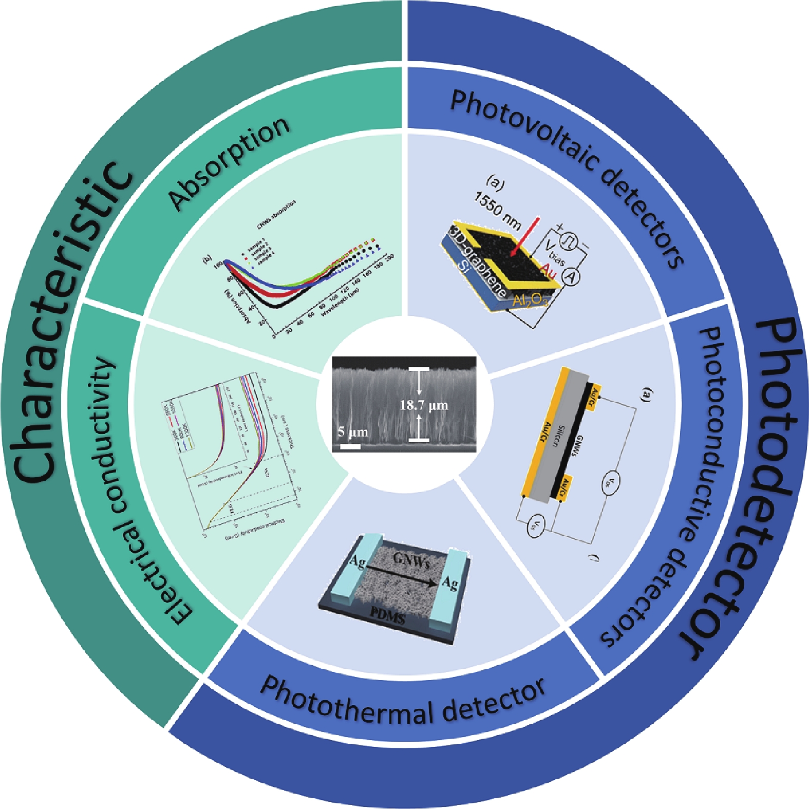
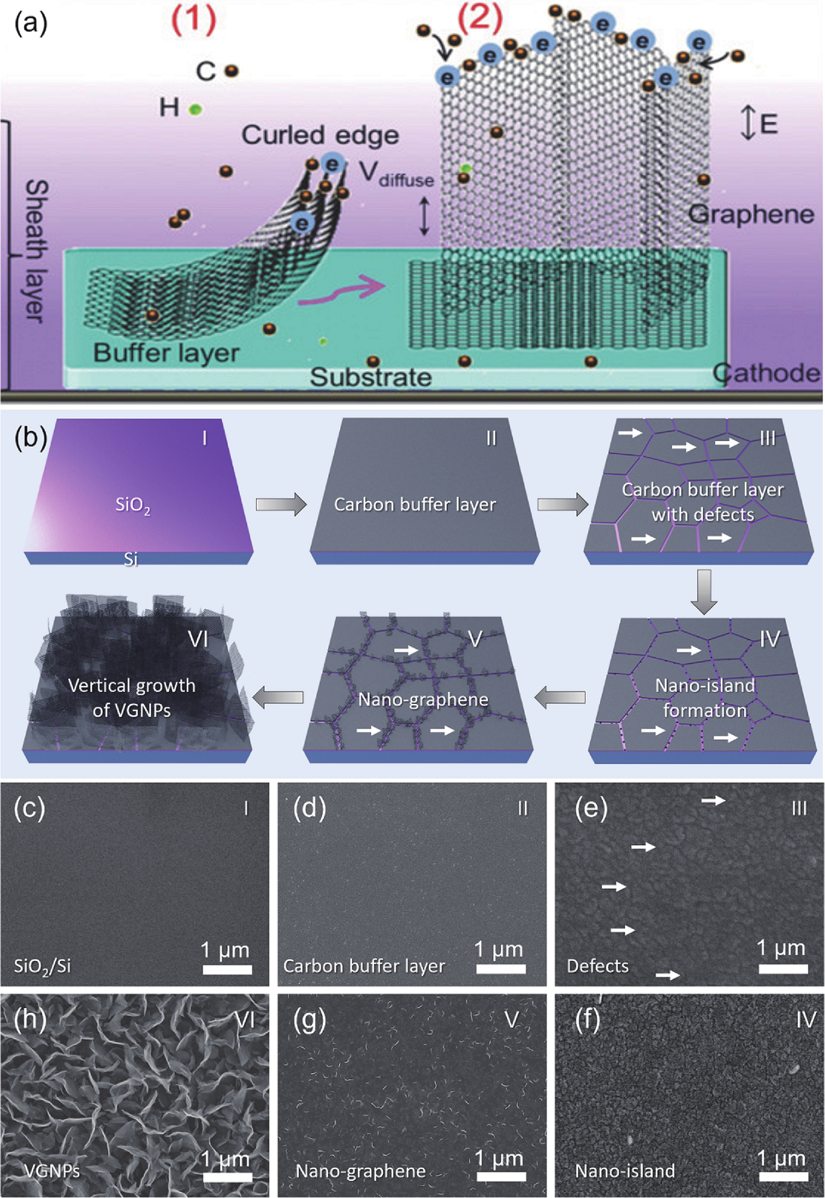
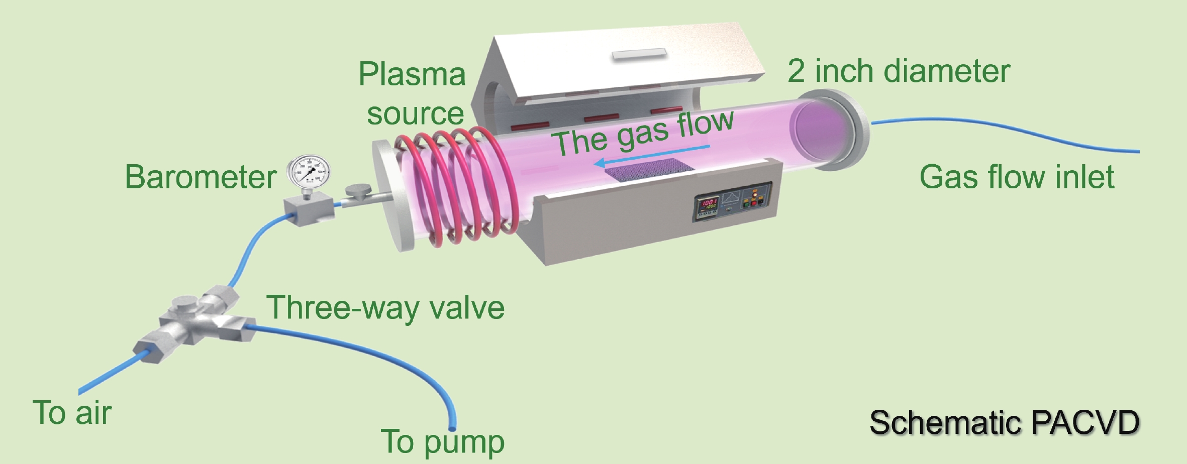
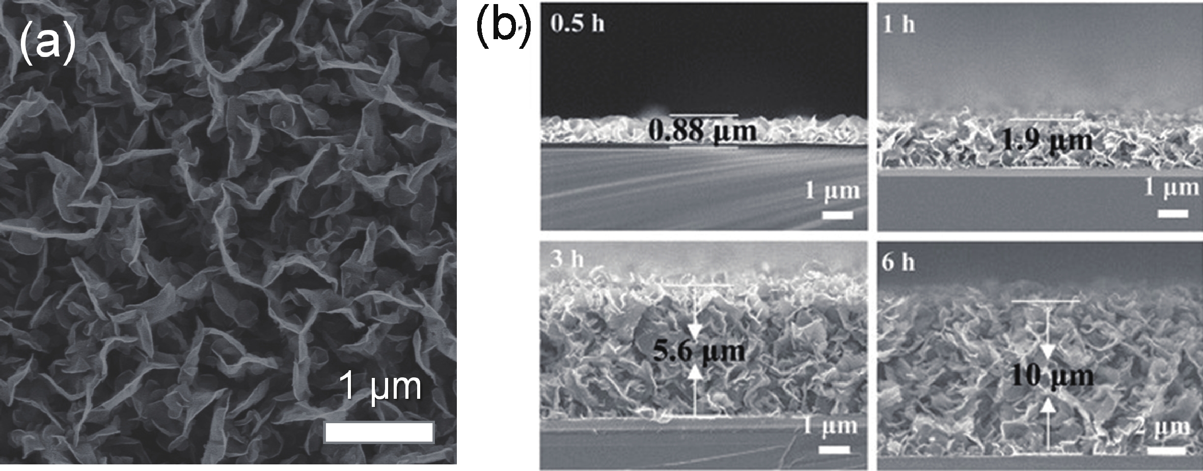
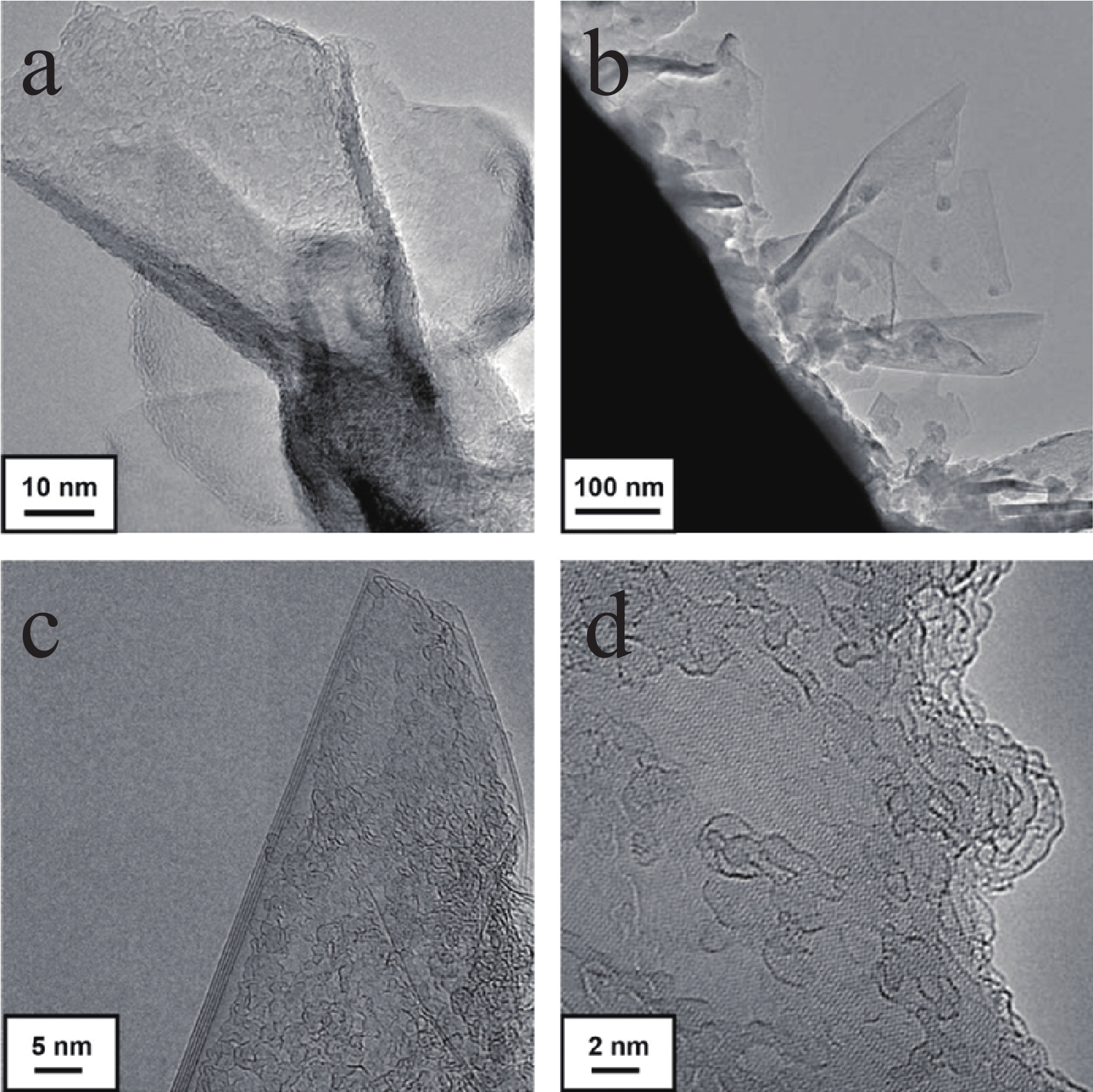
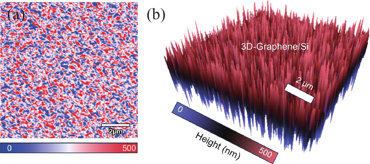
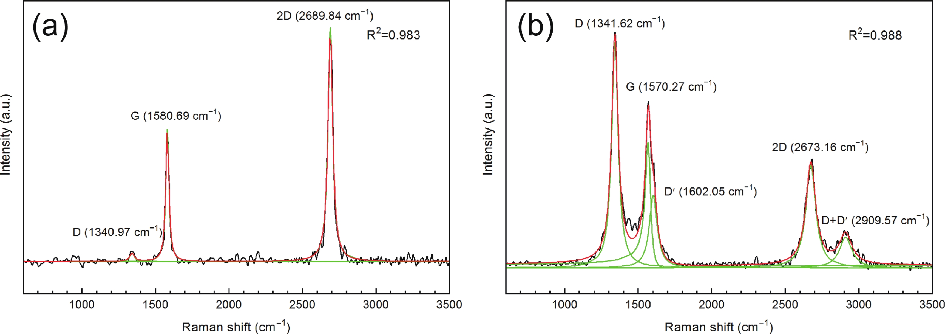
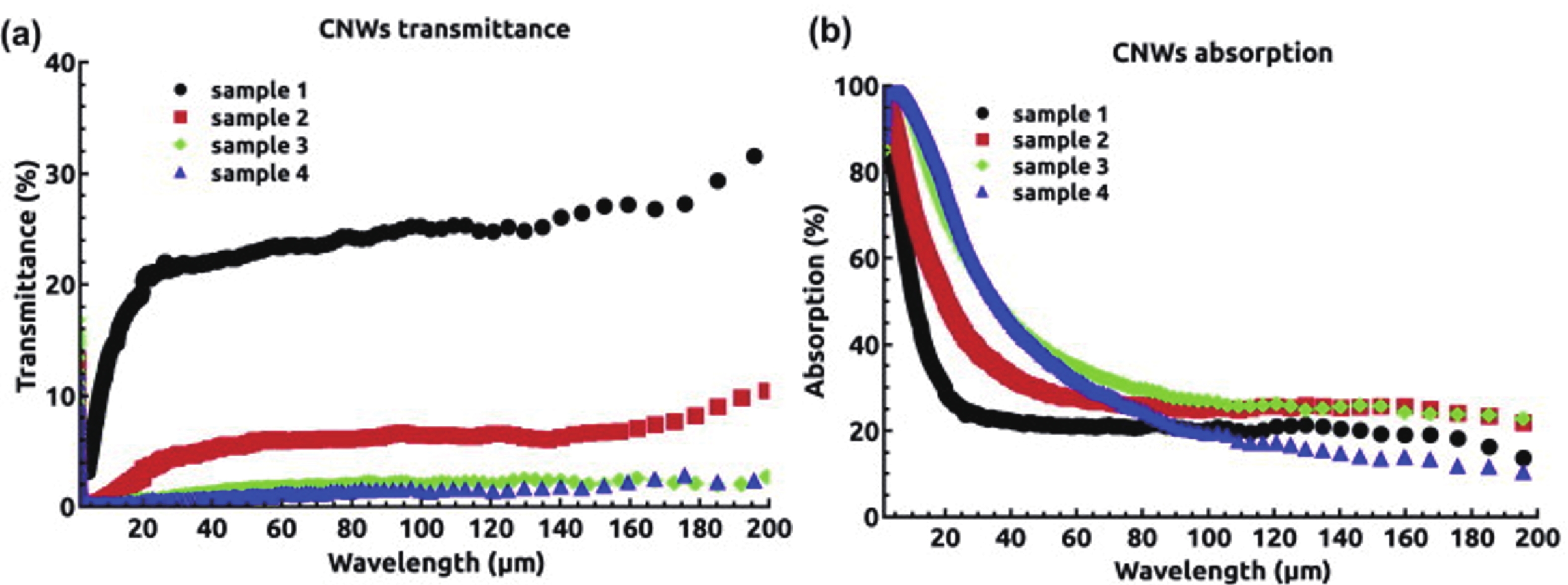
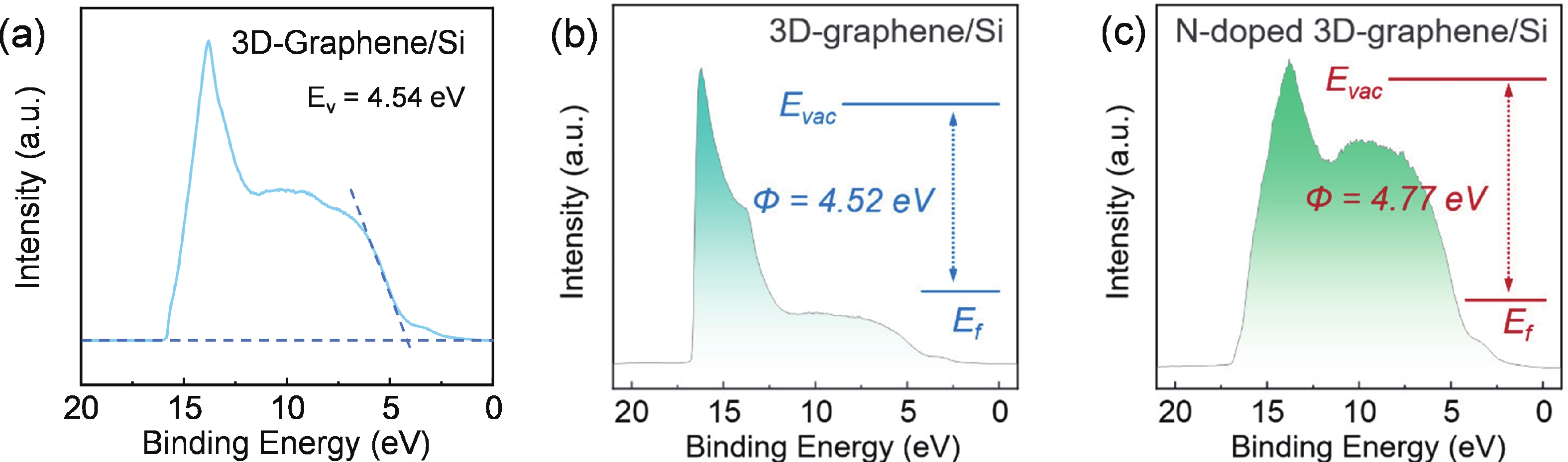
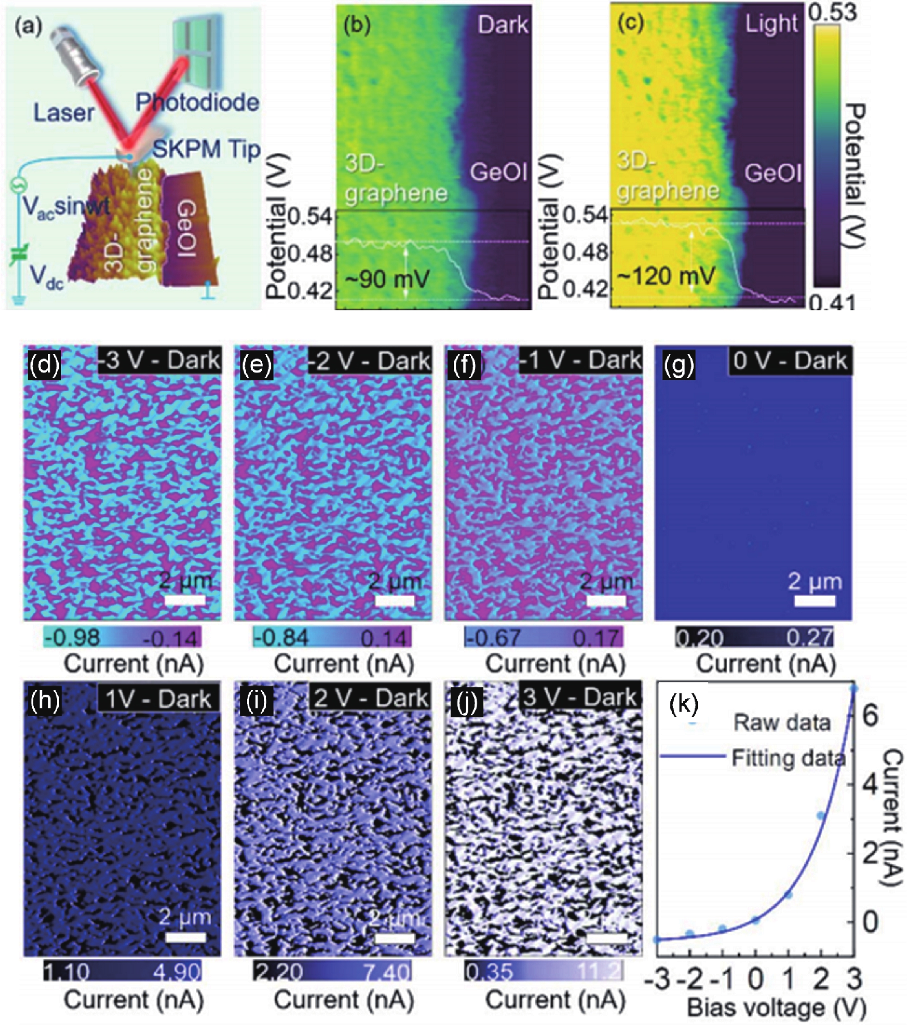
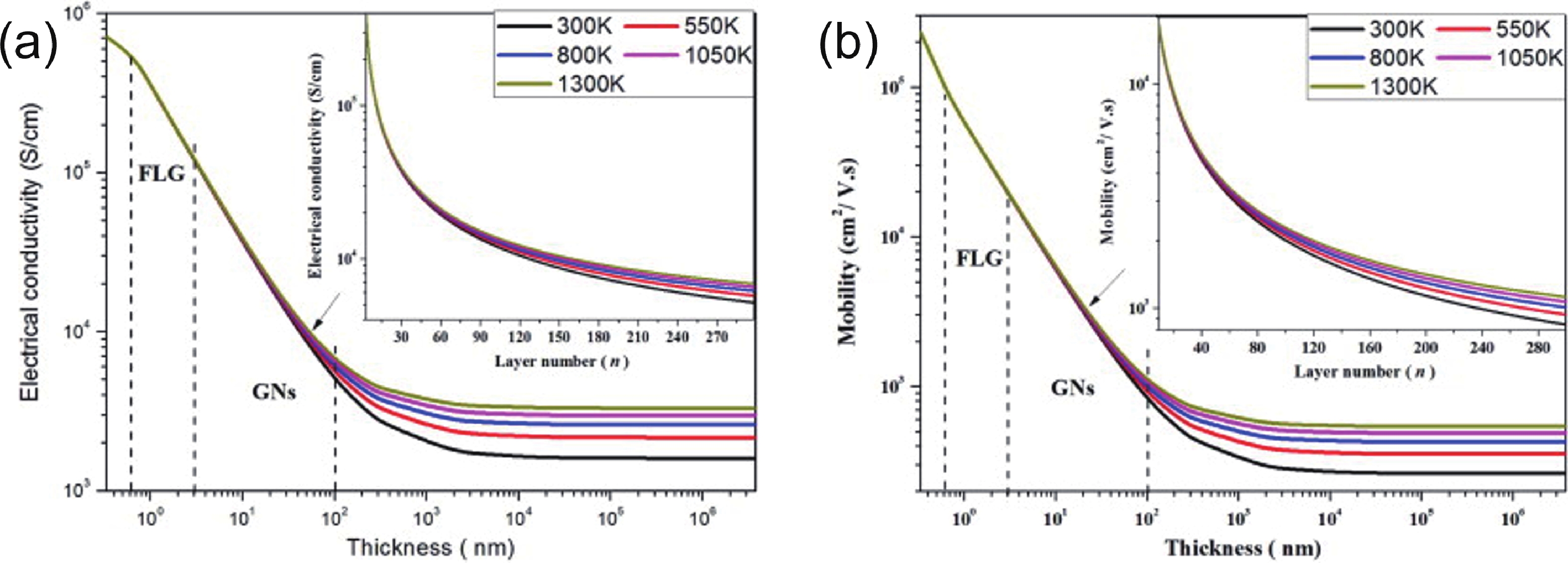
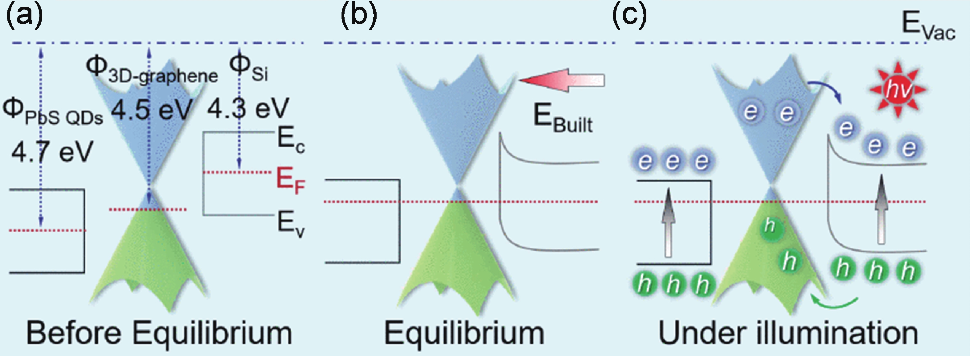
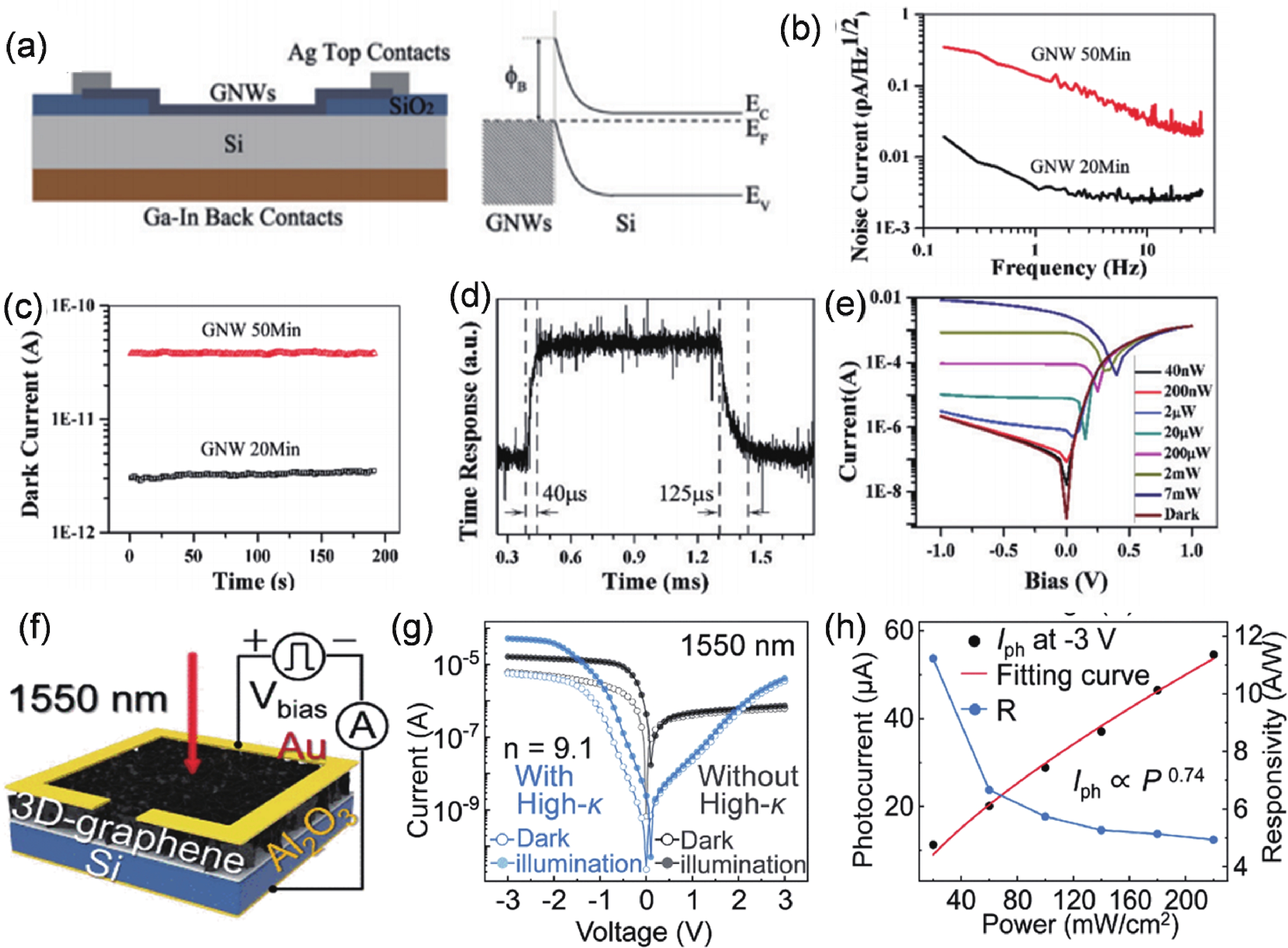
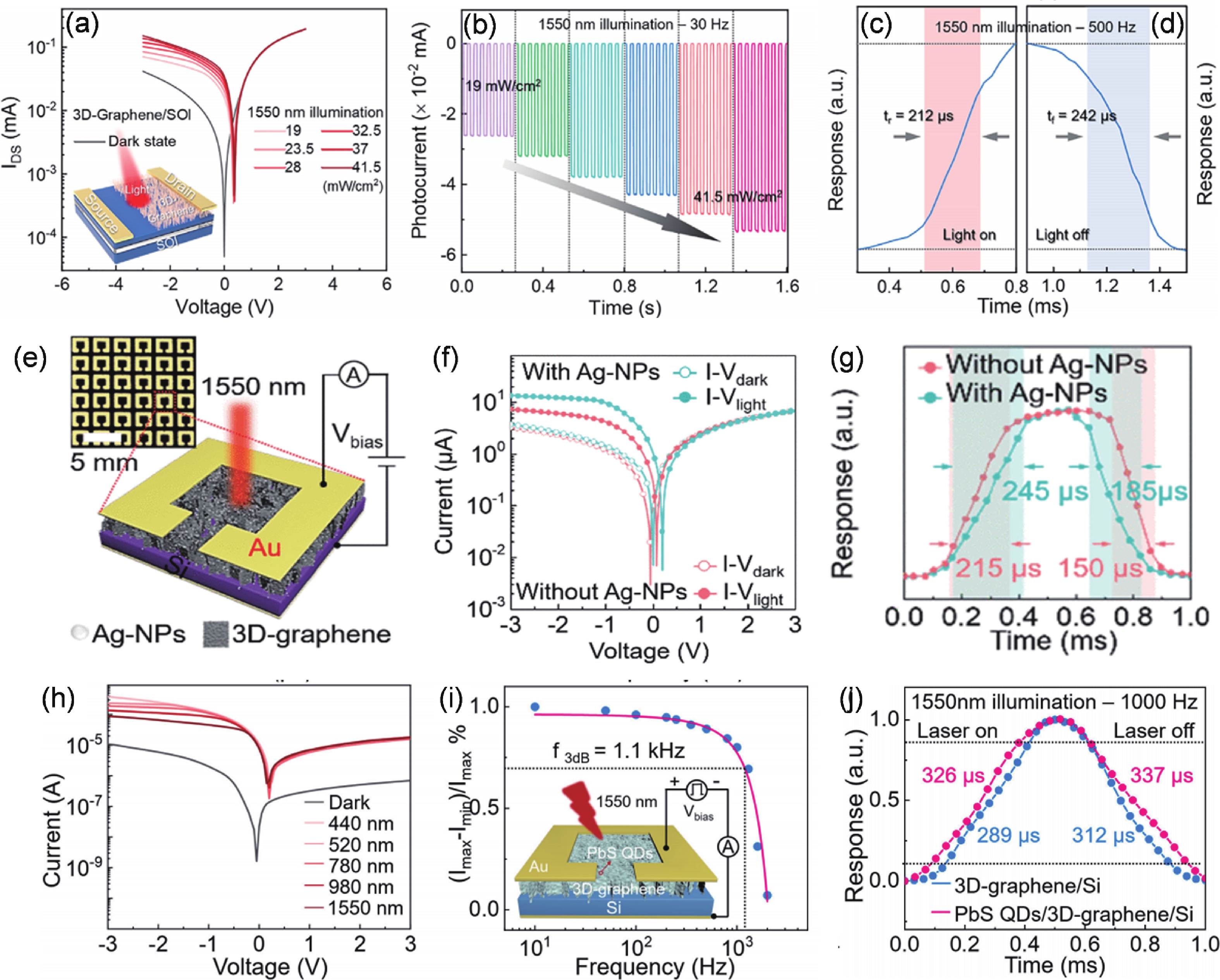
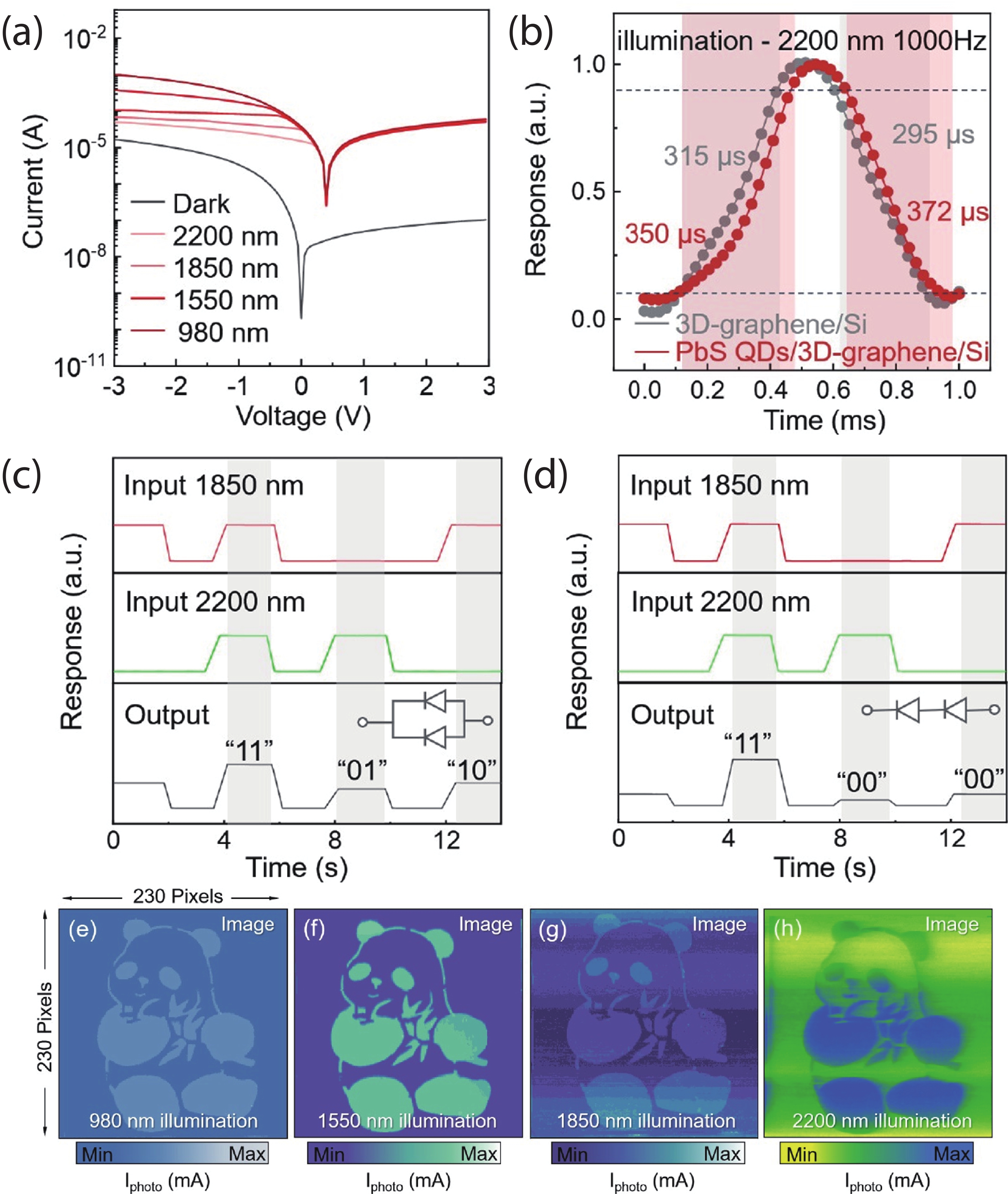
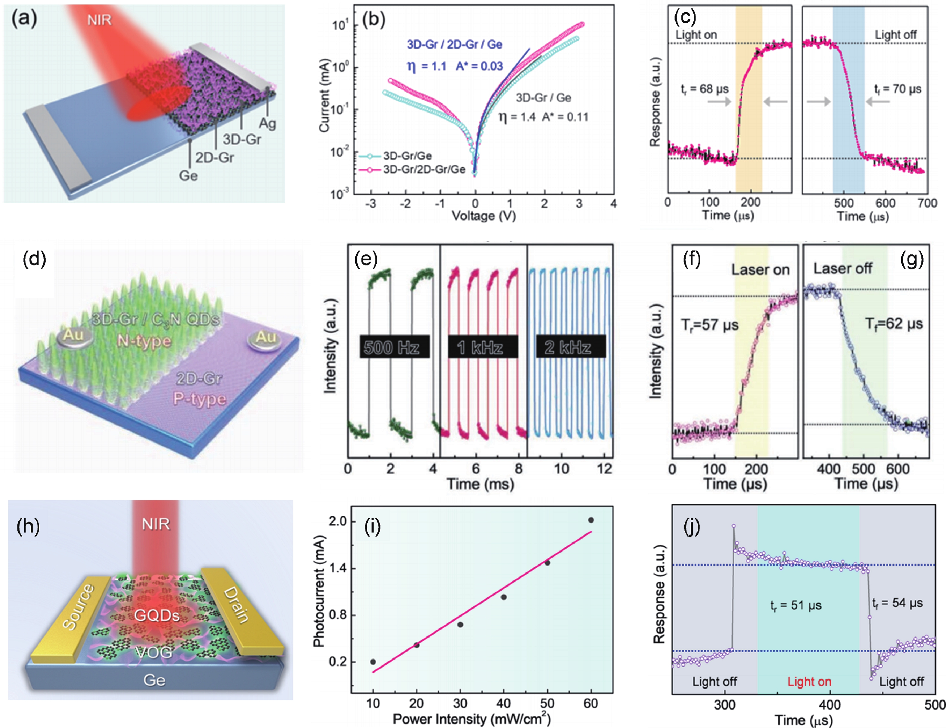
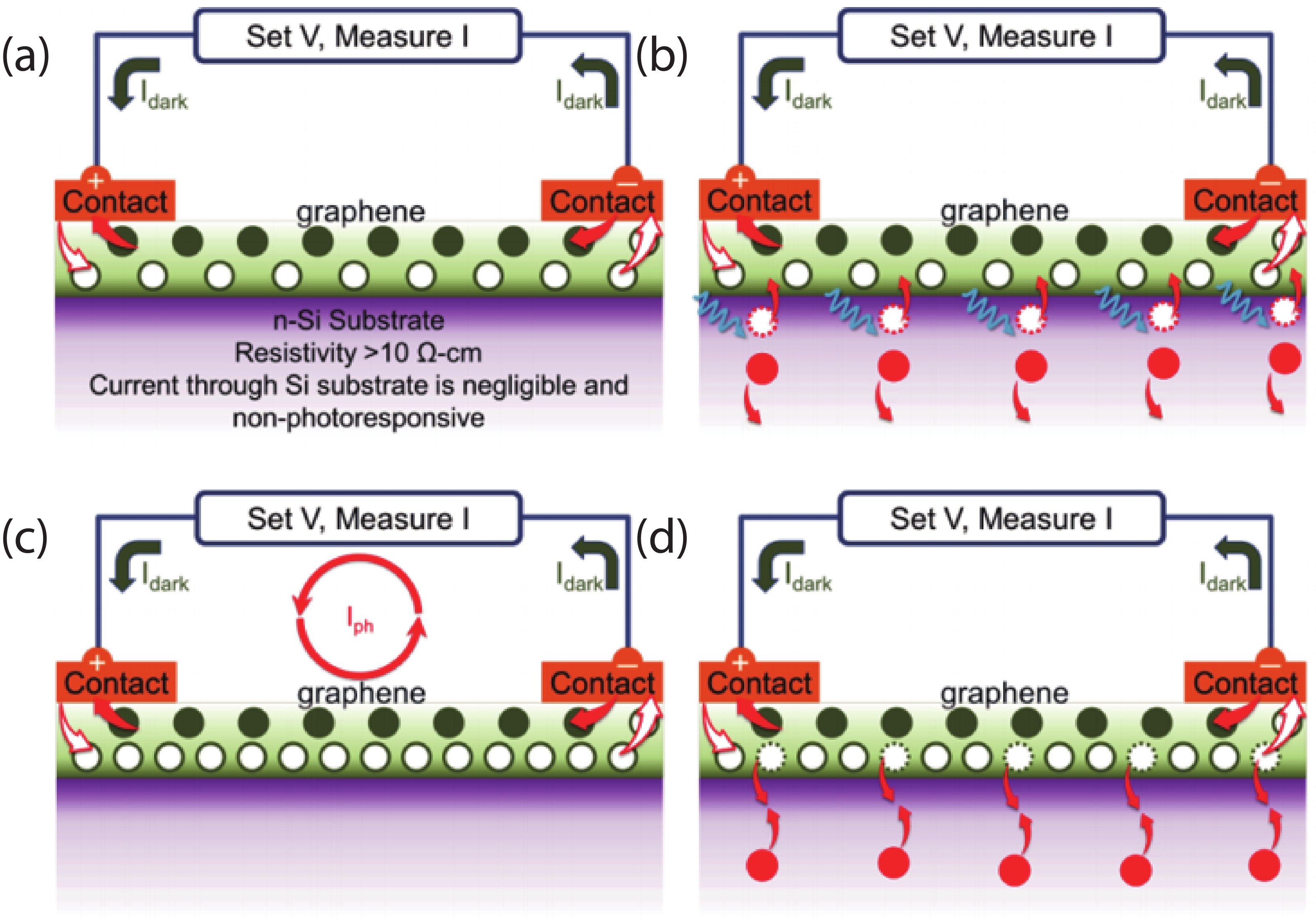
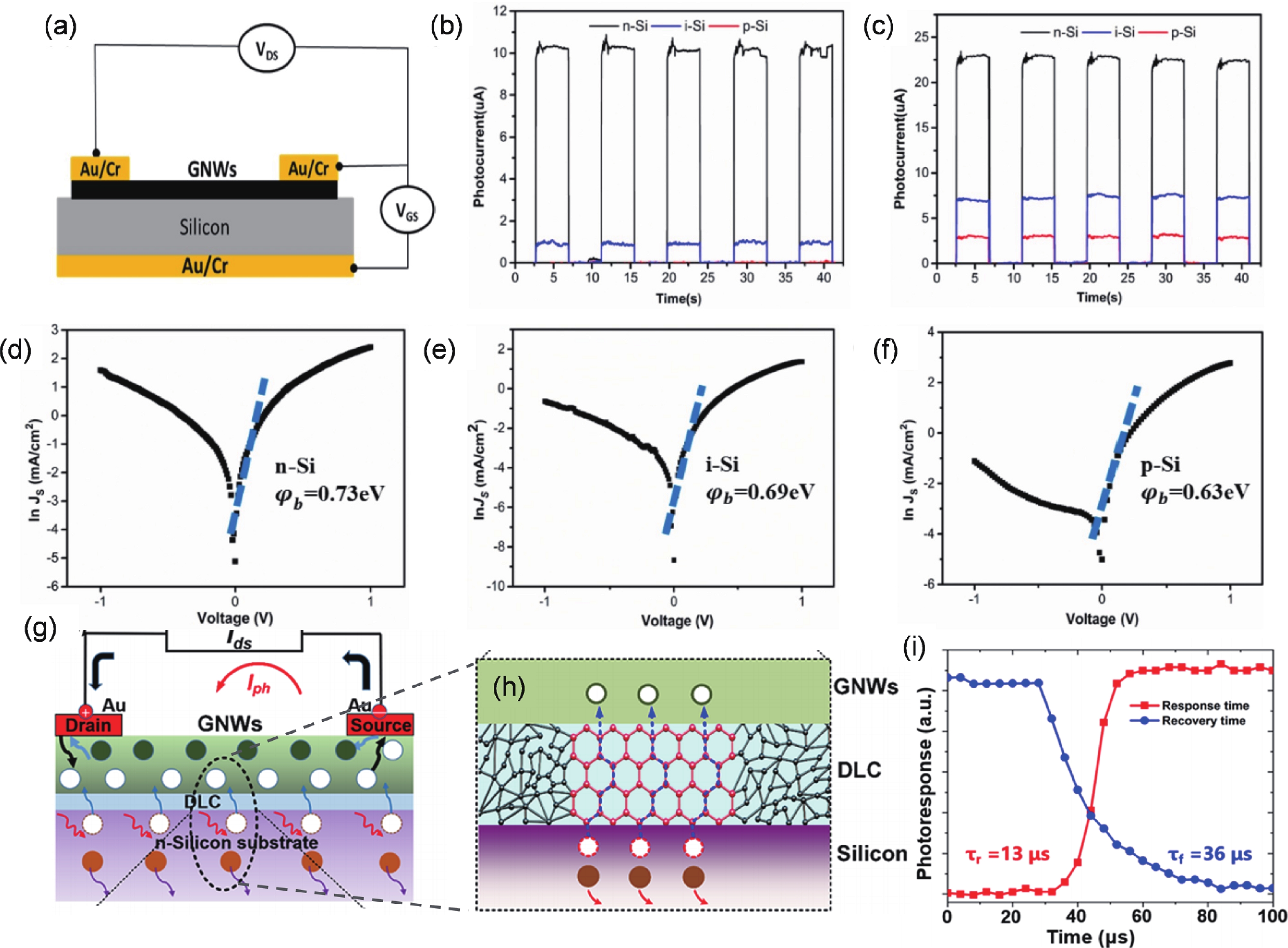
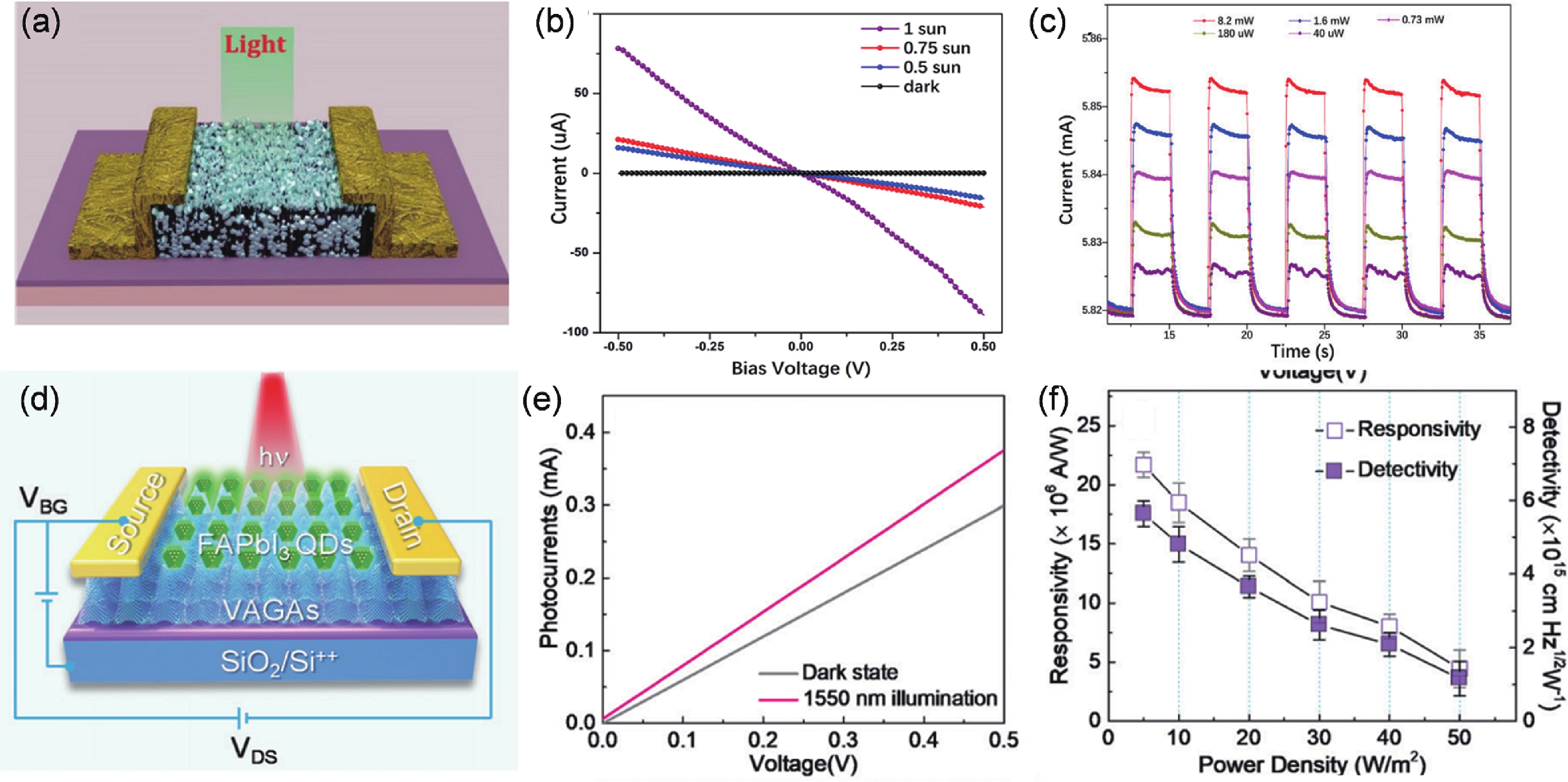
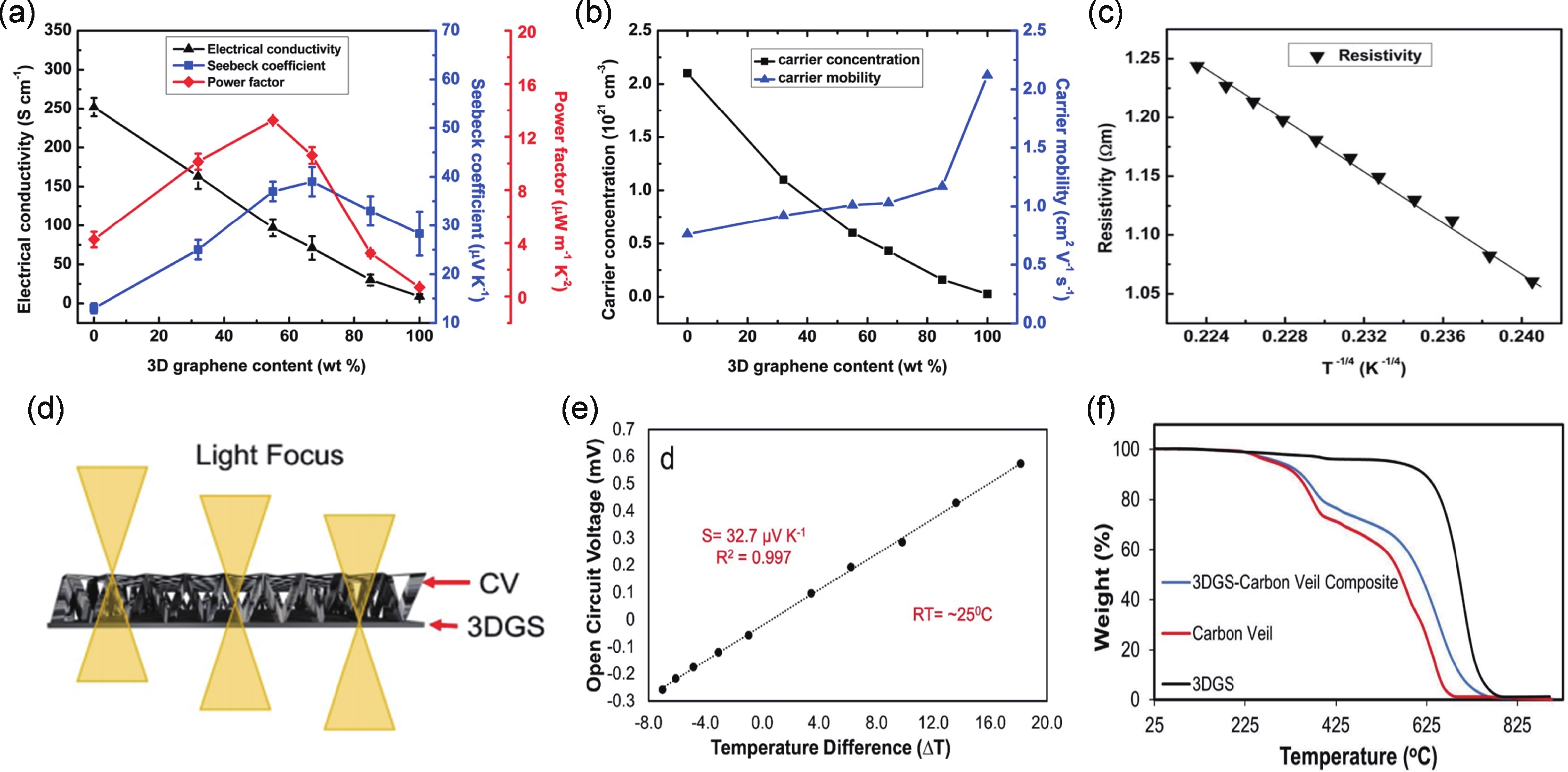
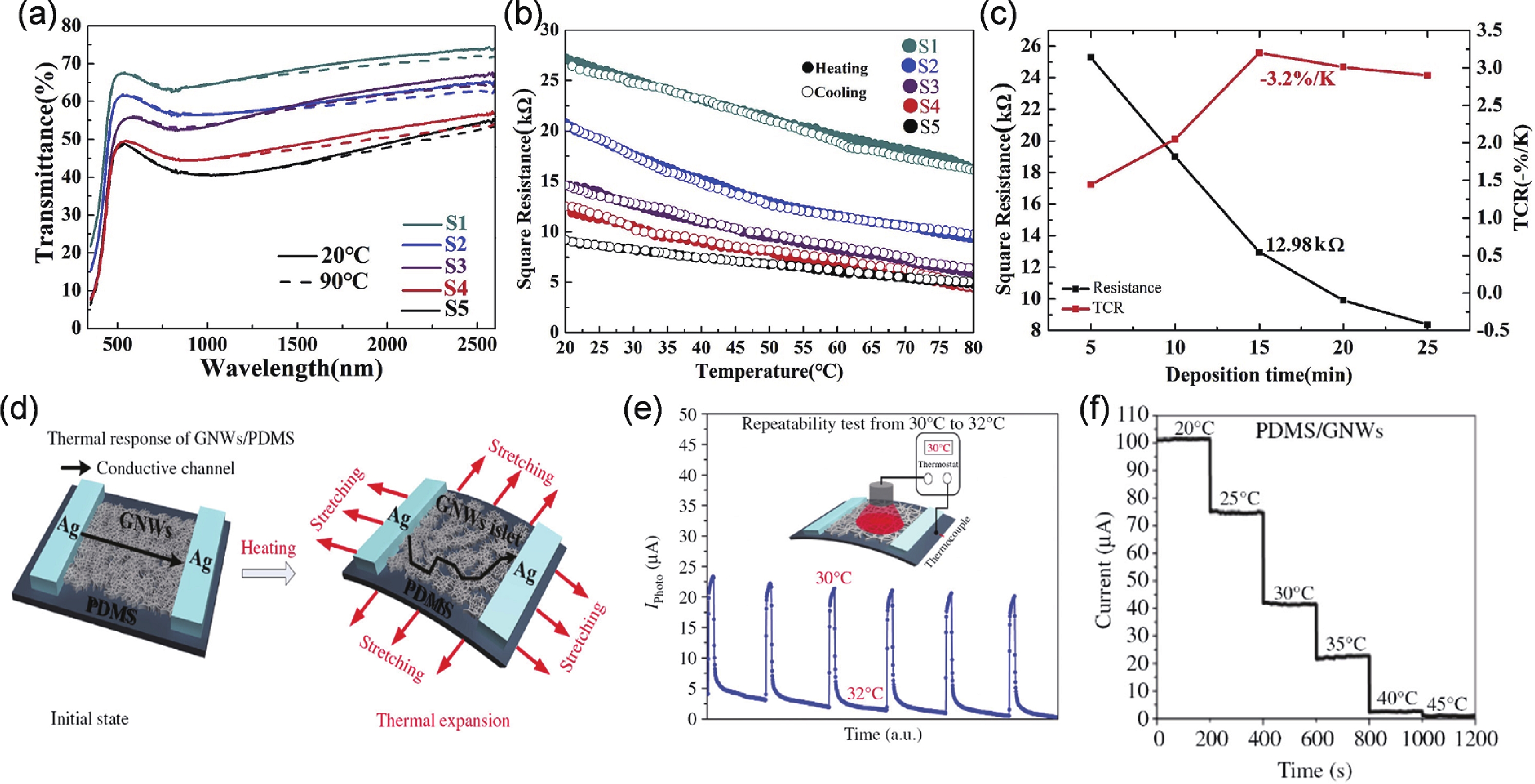
Graphene has garnered significant attention in photodetection due to its exceptional optical, electrical, mechanical, and thermal properties. However, the practical application of two-dimensional (2D) graphene in optoelectronic fields is limited by its weak light absorption (only 2.3%) and zero bandgap characteristics. Increasing light absorption is a critical scientific challenge for developing high-performance graphene-based photodetectors. Three-dimensional (3D) graphene comprises vertically grown stacked 2D-graphene layers and features a distinctive porous structure. Unlike 2D-graphene, 3D-graphene offers a larger specific surface area, improved electrochemical activity, and high chemical stability, making it a promising material for optoelectronic detection. Importantly, 3D-graphene has an optical microcavity structure that enhances light absorption through interaction with incoming light. This paper systematically reviews and analyzes the current research status and challenges of 3D-graphene-based photodetectors, aiming to explore feasible development paths for these devices and promote their industrial application.
J. Semicond.
2025, 46(7): 071701 doi: 10.1088/1674-4926/24100005

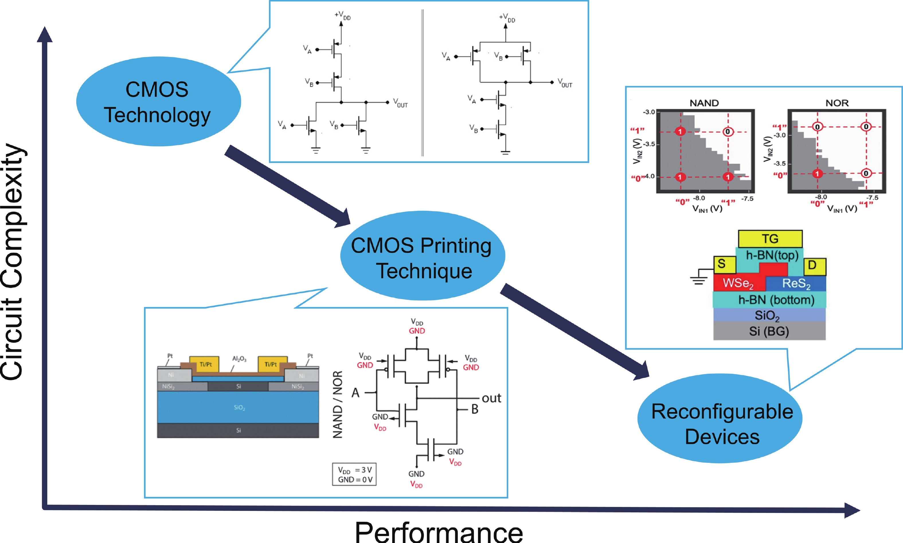
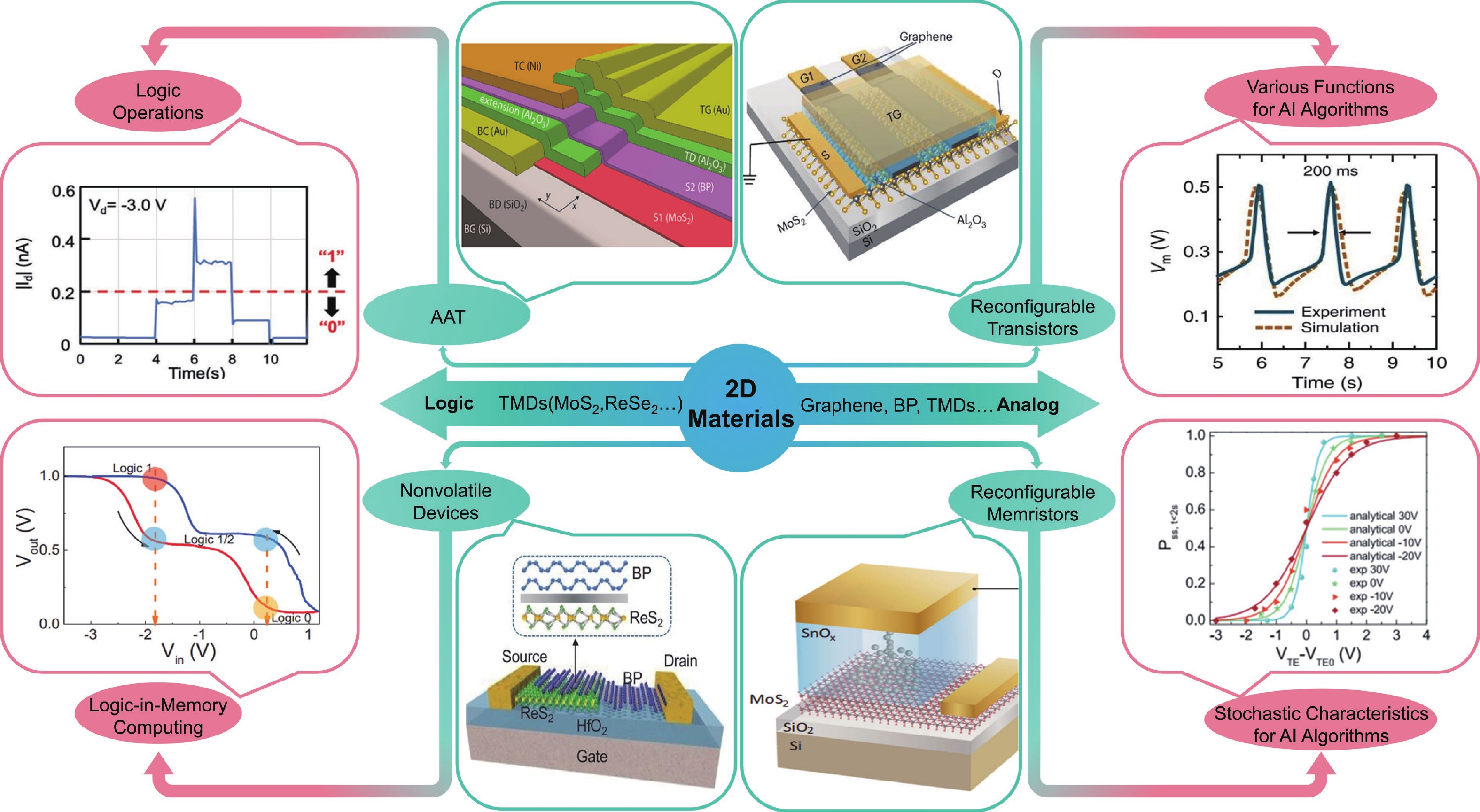
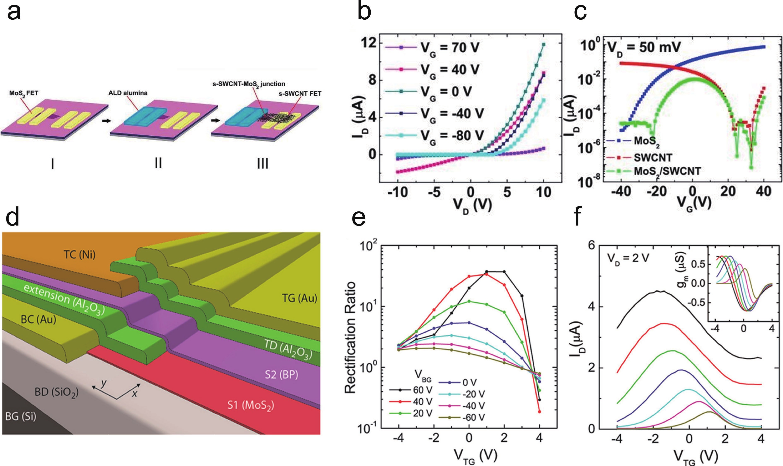
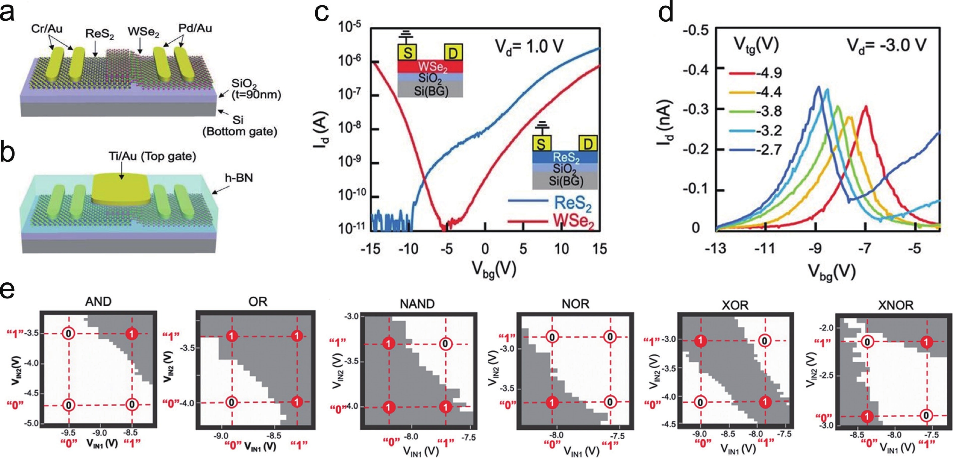
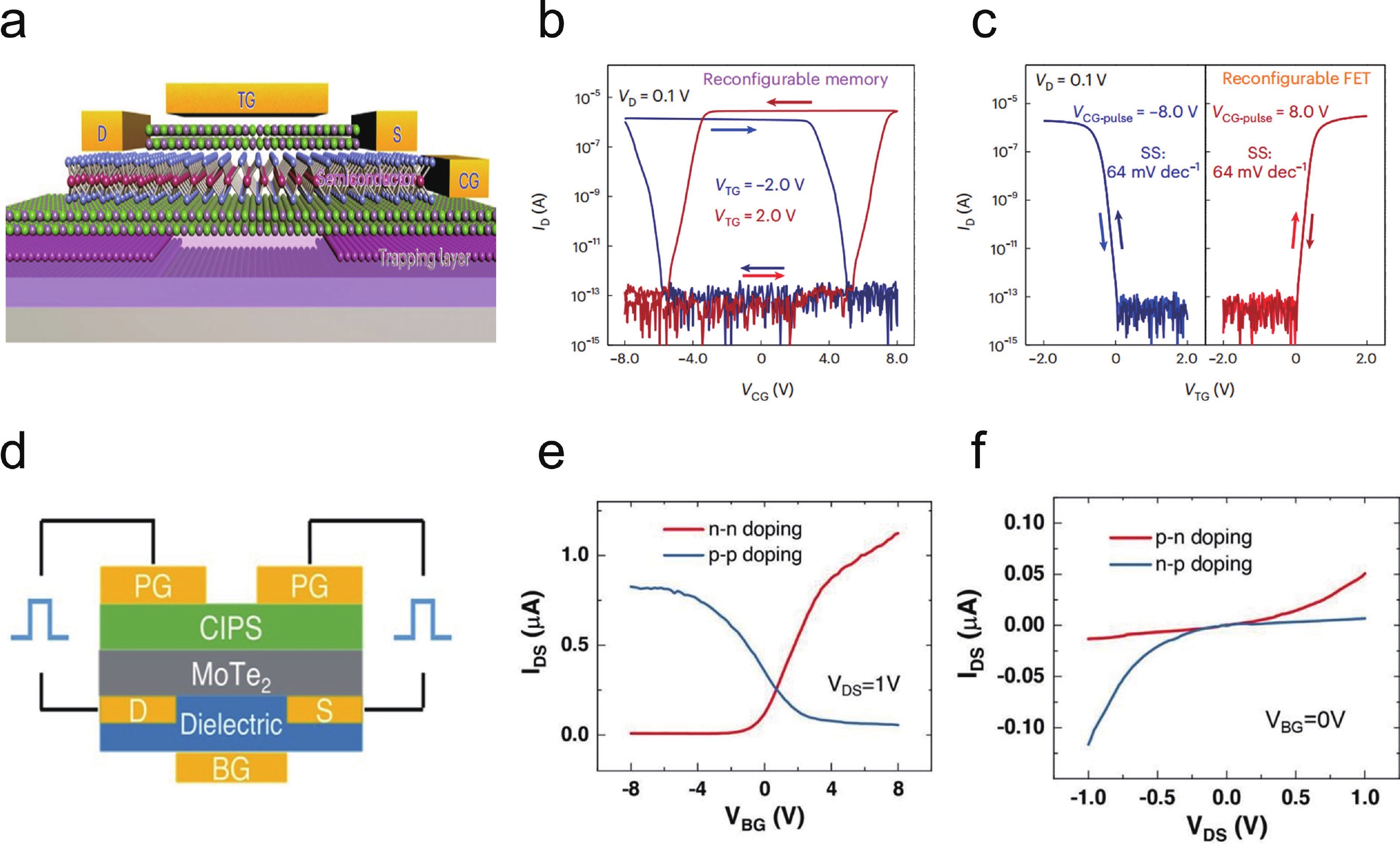
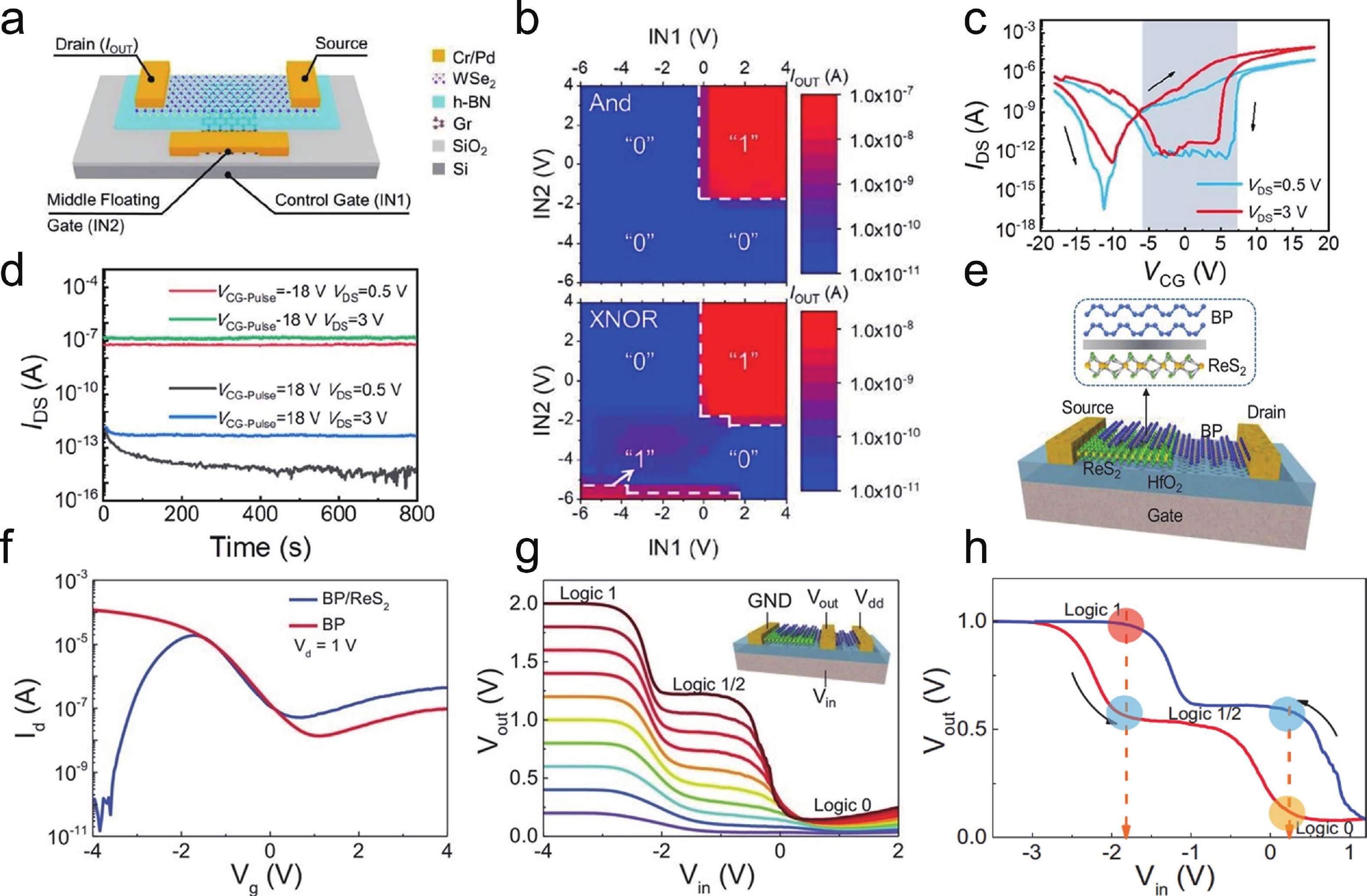
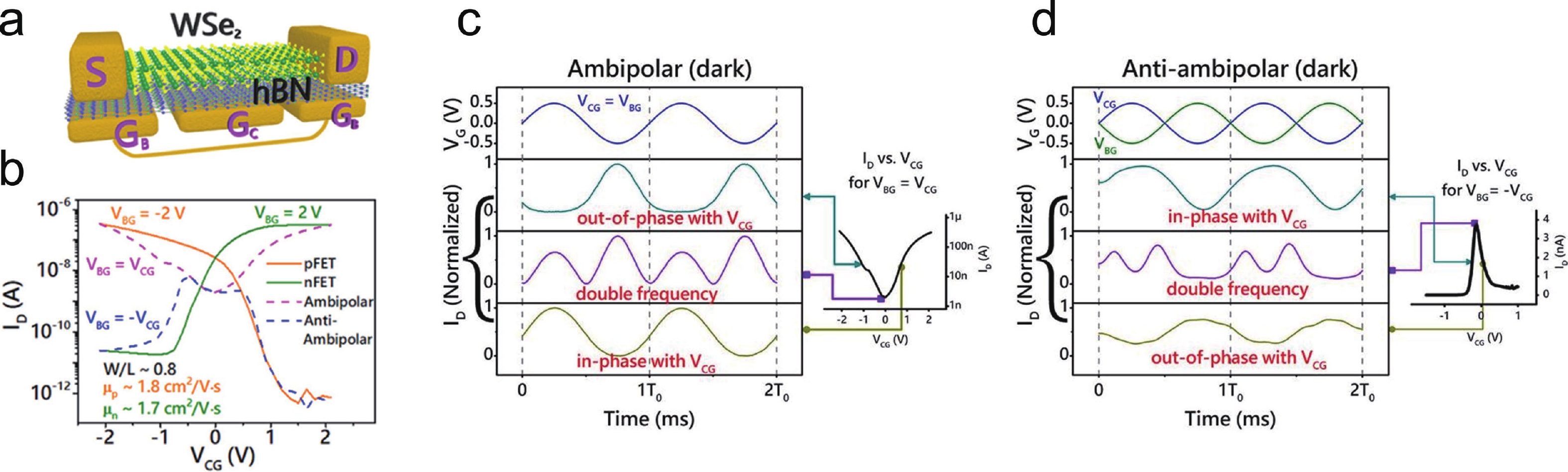
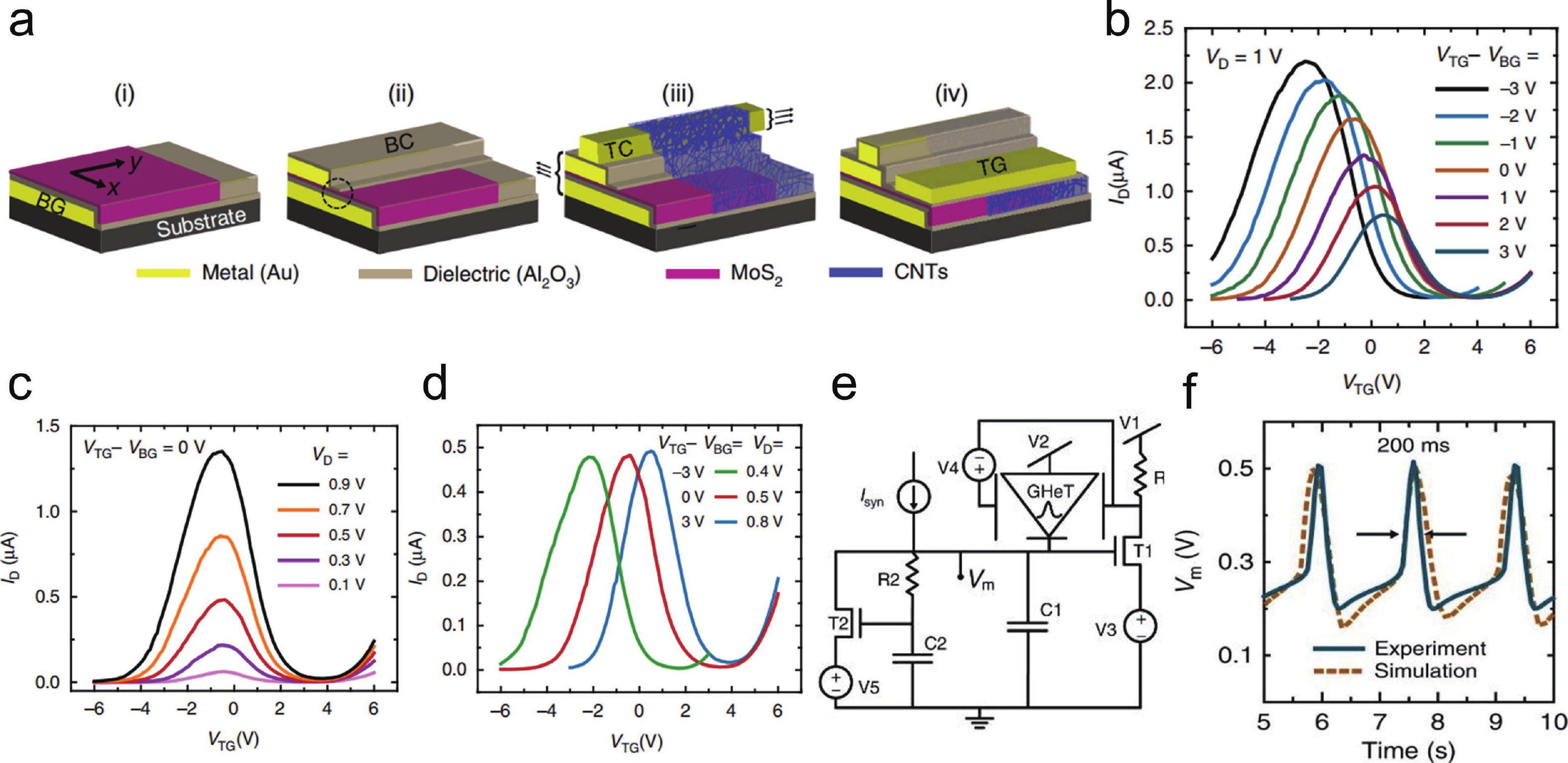
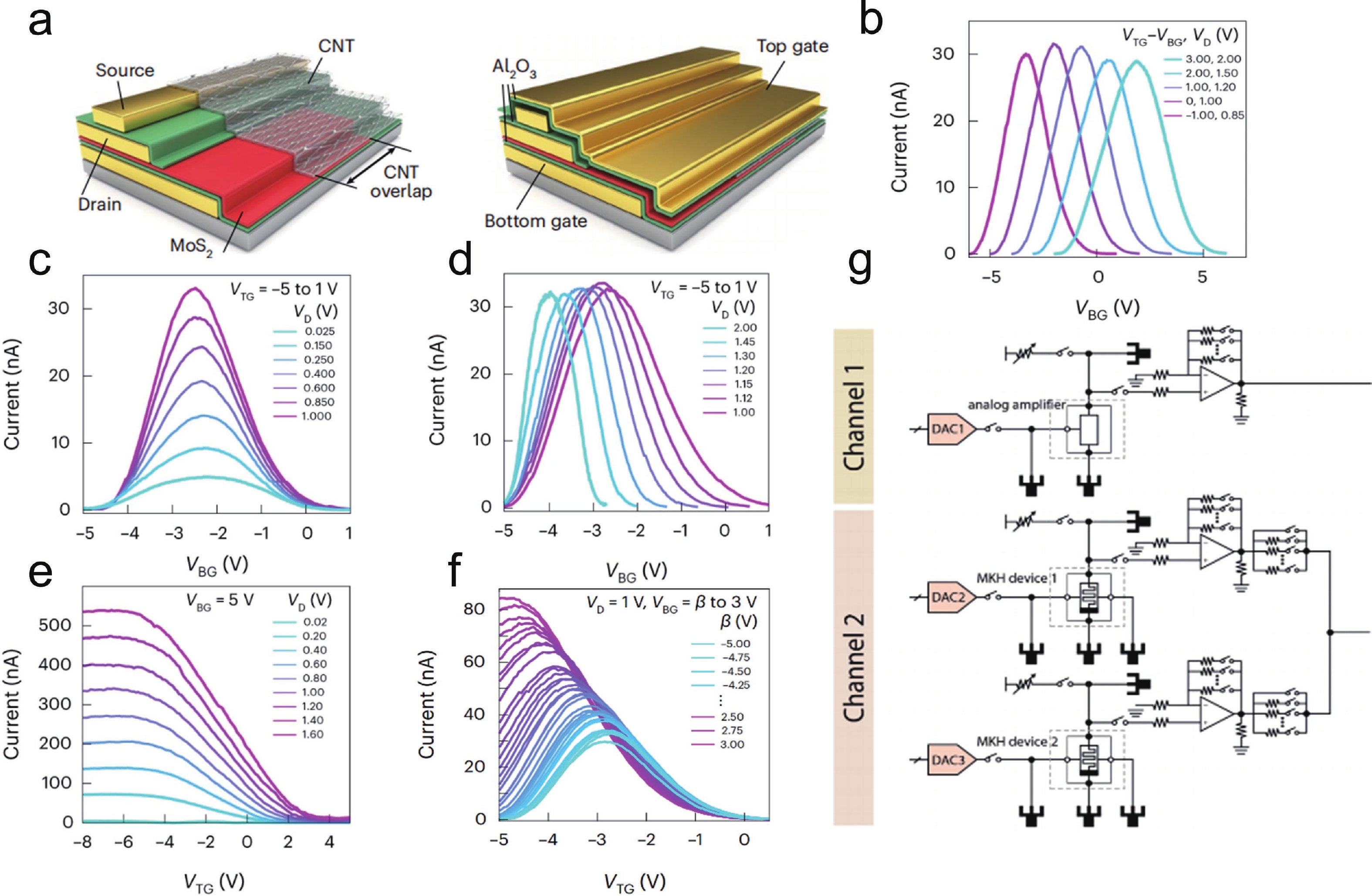
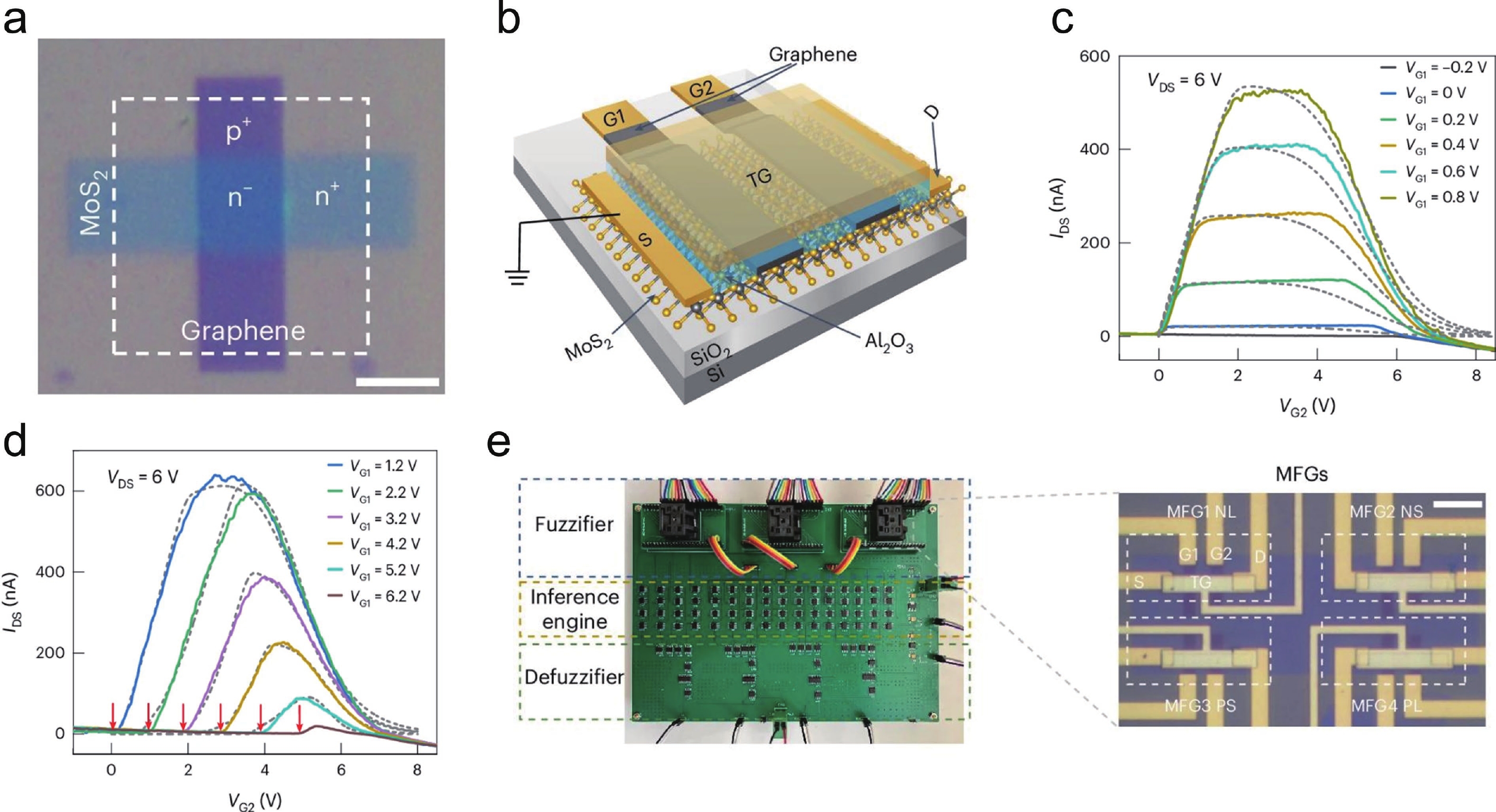
In recent years, as the dimensions of the conventional semiconductor technology is approaching the physical limits, while the multifunction circuits are restricted by the relatively fixed characteristics of the traditional metal−oxide−semiconductor field-effect transistors, reconfigurable devices that can realize reconfigurable characteristics and multiple functions at device level have been seen as a promising method to improve integration density and reduce power consumption. Owing to the ultrathin structure, effective control of the electronic characteristics and ability to modulate structural defects, two-dimensional (2D) materials have been widely used to fabricate reconfigurable devices. In this review, we summarize the working principles and related logic applications of reconfigurable devices based on 2D materials, including generating tunable anti-ambipolar responses and demonstrating nonvolatile operations. Furthermore, we discuss the analog signal processing applications of anti-ambipolar transistors and the artificial intelligence hardware implementations based on reconfigurable transistors and memristors, respectively, therefore highlighting the outstanding advantages of reconfigurable devices in footprint, energy consumption and performance. Finally, we discuss the challenges of the 2D materials-based reconfigurable devices.
J. Semicond.
2025, 46(7): 072101 doi: 10.1088/1674-4926/24090005
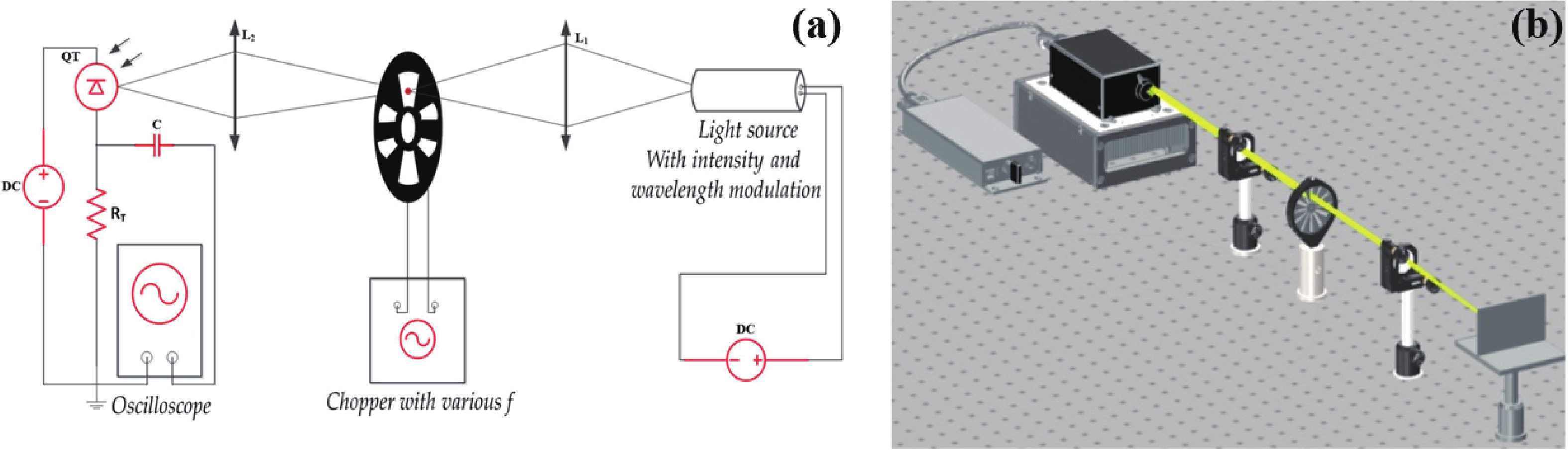
Minority carrier lifetimes τ are a fundamental parameter in semiconductor devices, representing the average time it takes for excess minority carriers to recombine. This characteristic is crucial for understanding and optimizing the performance of semiconductor materials, as it directly influences charge carrier dynamics and overall device efficiency. This work presents a development of PbS thin film deposited by thermal evaporation, at which the PbS thin film was further employed for structural, optical properties, and τ. Especially, the PbS film is probed with an in-house setup for identifying the τ. The procedure is to subject the PbS thin film with a flashlight from a light source with a middle rotating frequency. The derived τ in the in-house characterization setup agrees well with the value from the higher cost characterizing approach of photoluminescence. Therefore, the in-house setup provides additional tools for identifying the τ values for semiconductor devices.
J. Semicond.
2025, 46(7): 072102 doi: 10.1088/1674-4926/24110034
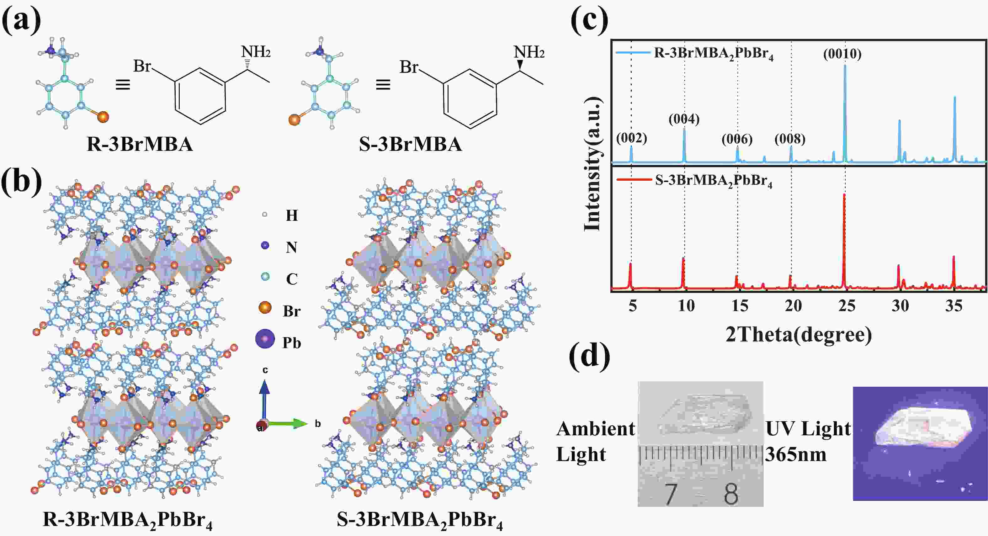
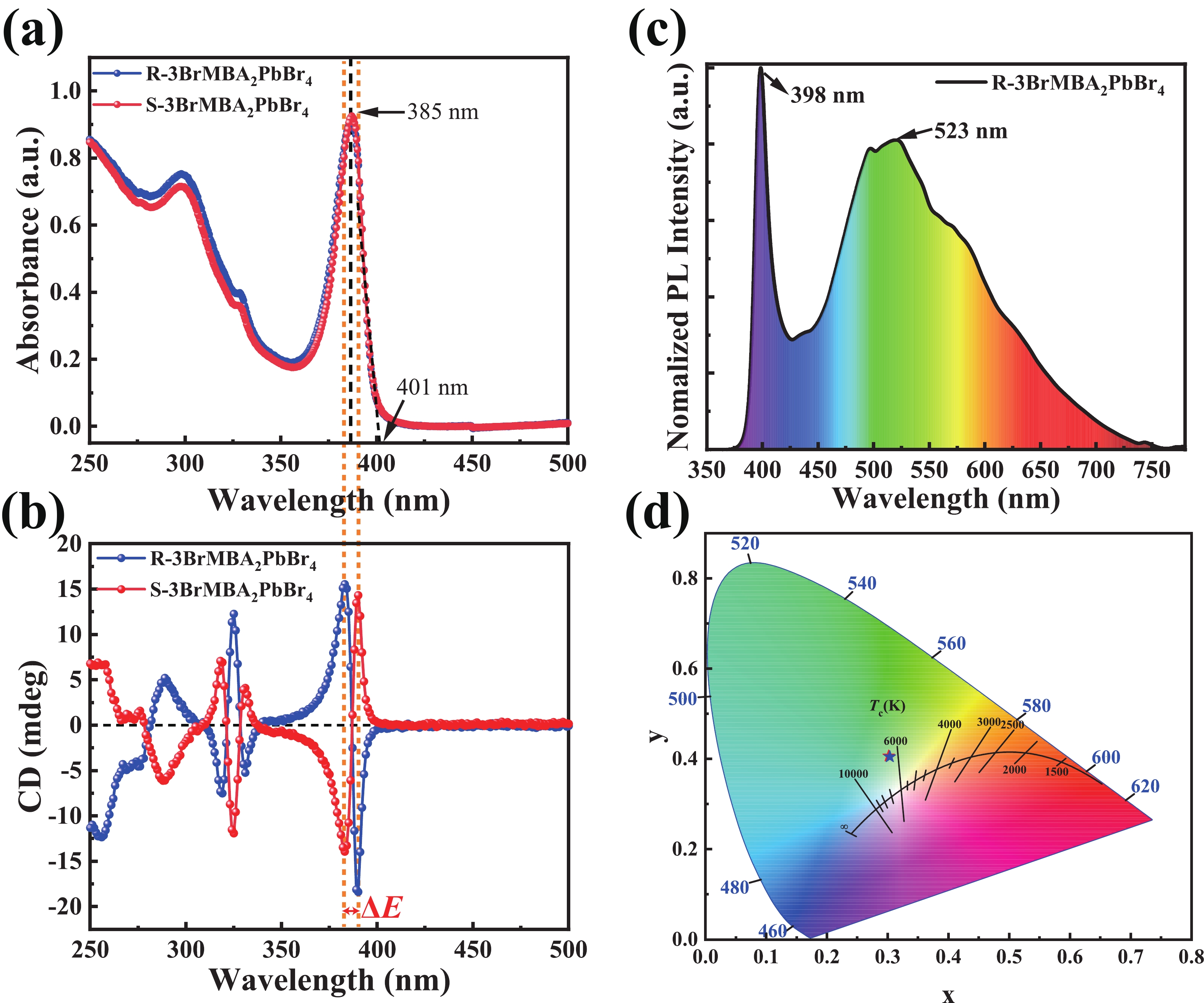
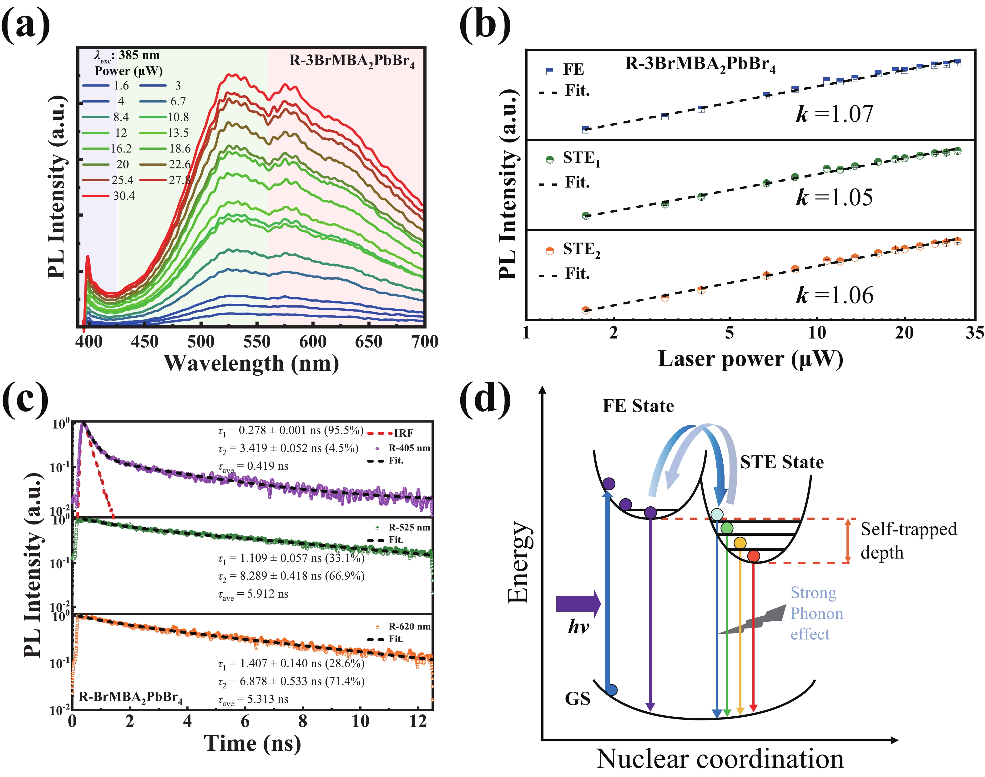
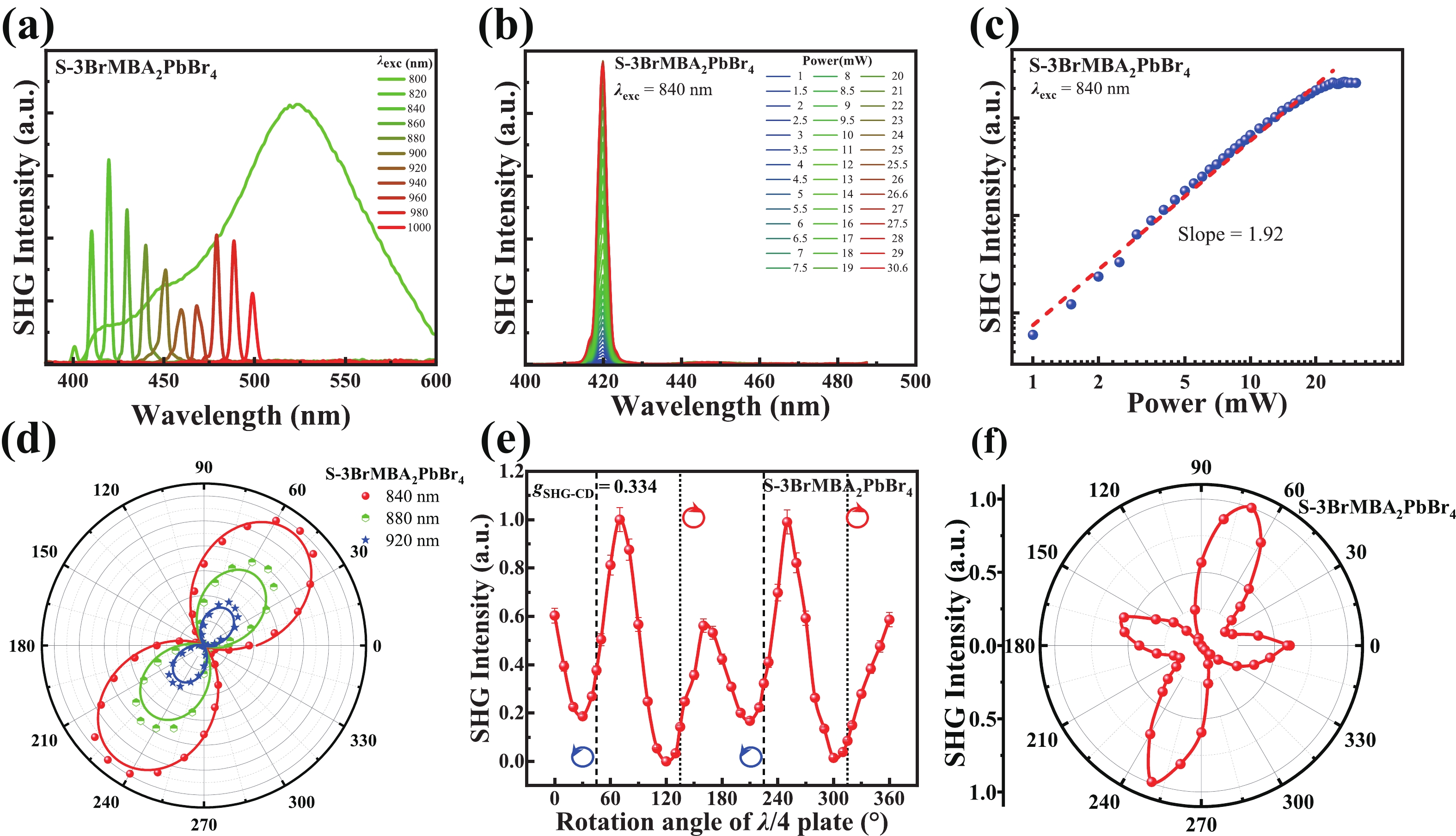
Two-dimensional (2D) chiral halide perovskites (CHPs) have attracted broad interest due to their distinct spin-dependent properties and promising applications in chiroptics and spintronics. Here, we report a new type of 2D CHP single crystals, namely R/S-3BrMBA2PbBr4. The chirality of the as-prepared samples is confirmed by exploiting circular dichroism spectroscopy, indicating a successful chirality transfer from chiral organic cations to their inorganic perovskite sublattices. Furthermore, we observed bright photoluminescence spanning from 380 to 750 nm in R/S-3BrMBA2PbBr4 crystals at room temperature. Such broad photoluminescence originates from free excitons and self-trapped excitons. In addition, efficient second-harmonic generation (SHG) performance was observed in chiral perovskite single crystals with high circular polarization ratios and non-linear optical circular dichroism. This demonstrates that R/S-3BrMBA2PbBr4 crystals can be used to detect and generate left- and right-handed circularly polarized light. Our study provides a new platform to develop high-performance chiroptical and spintronic devices.
J. Semicond.
2025, 46(7): 072501 doi: 10.1088/1674-4926/25010017
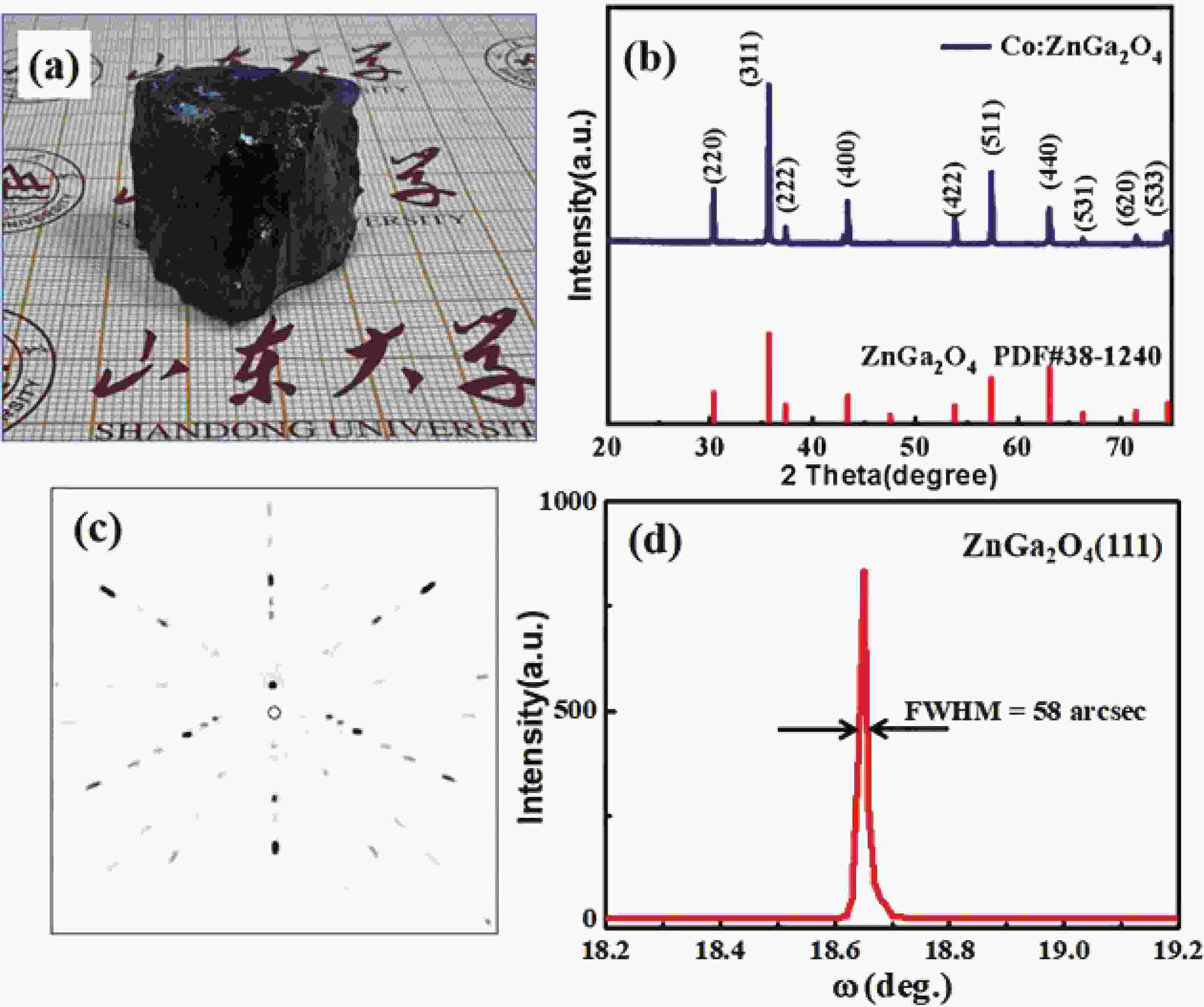
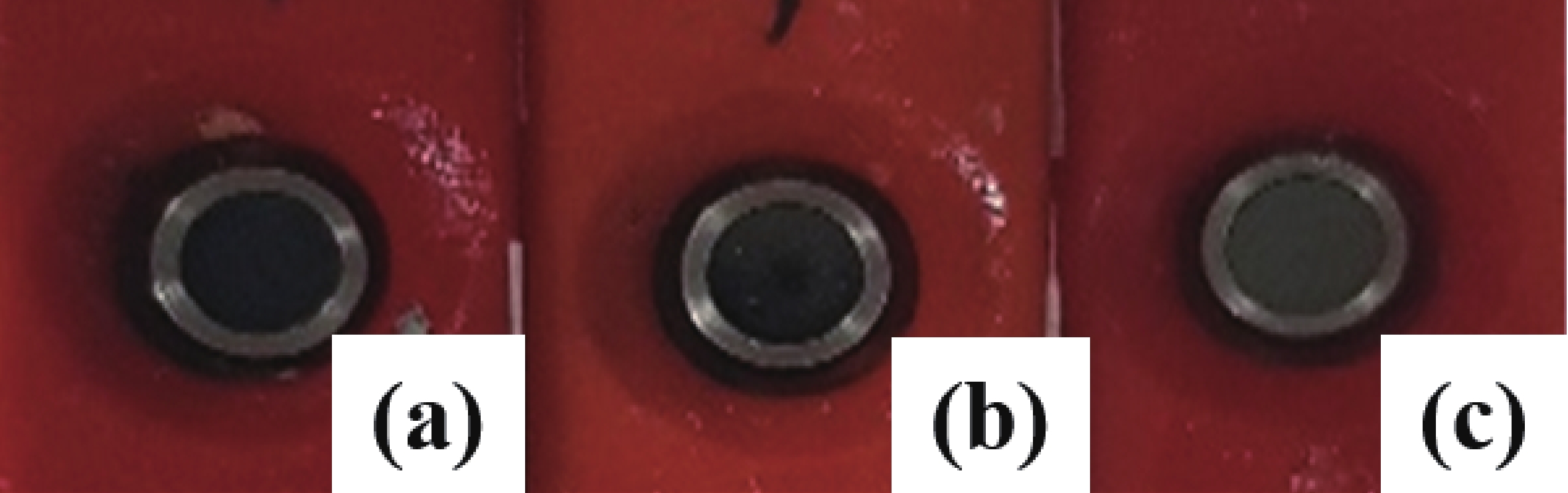
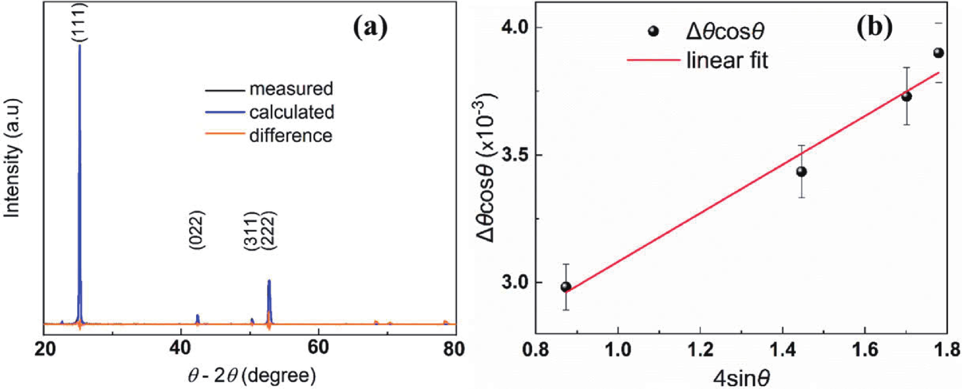
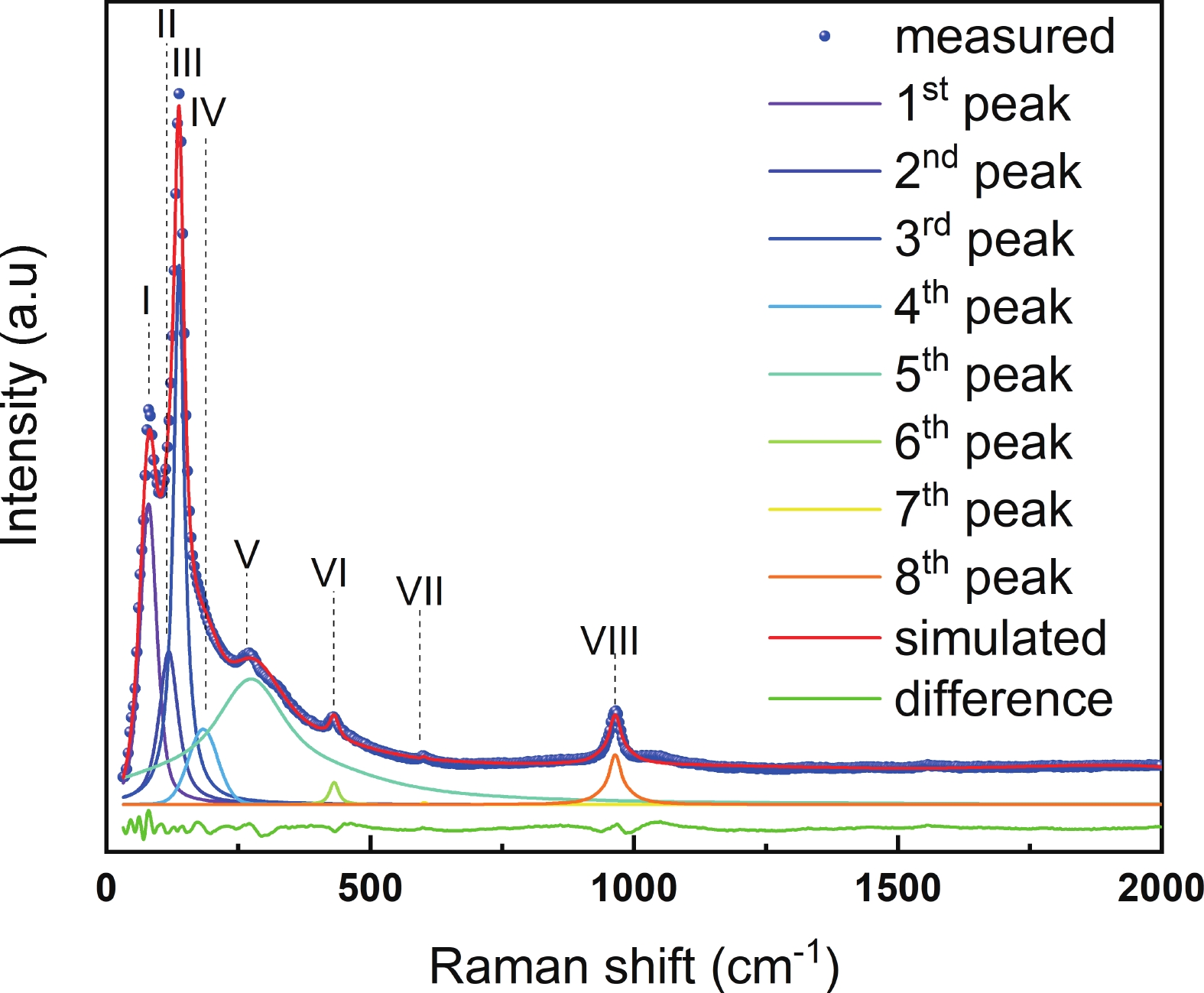
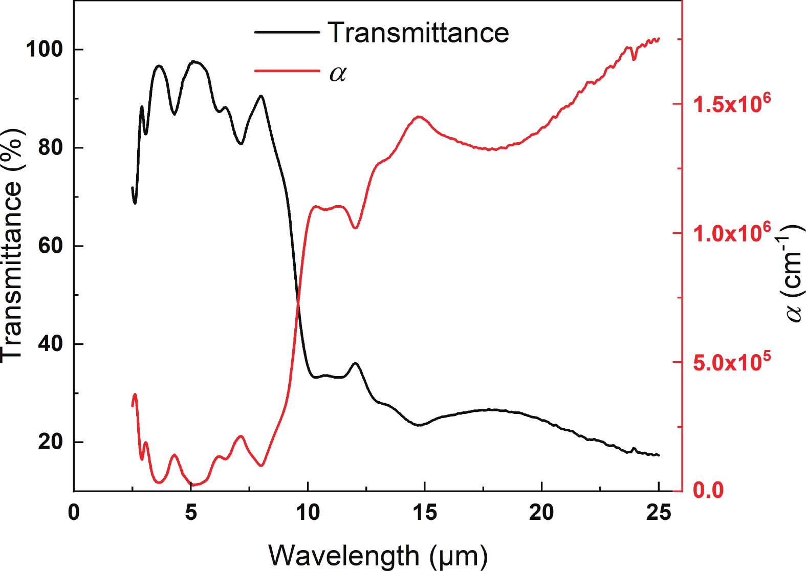
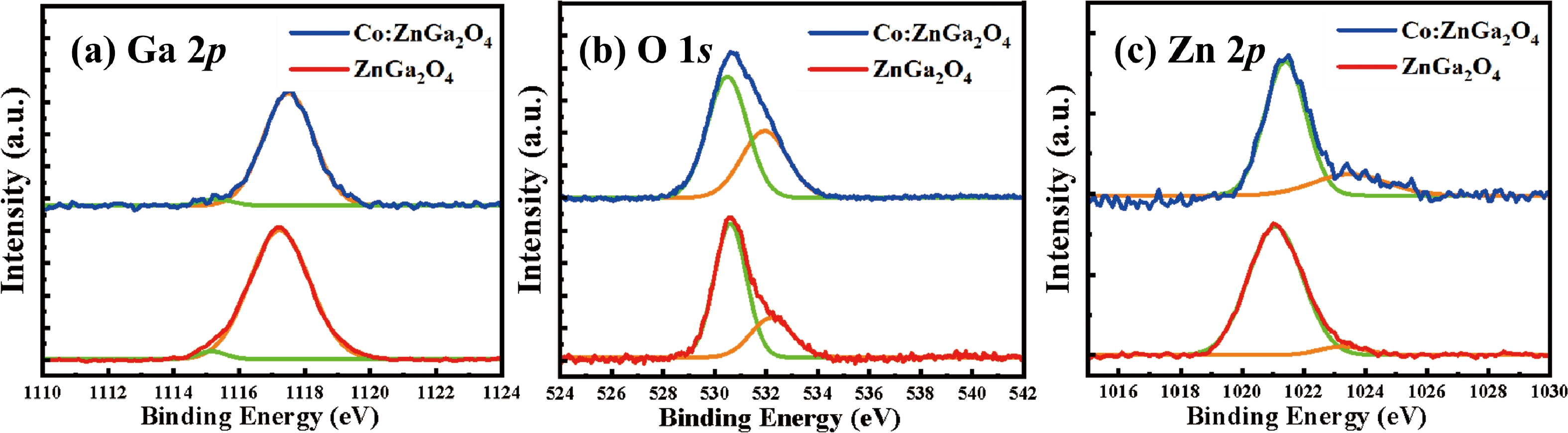
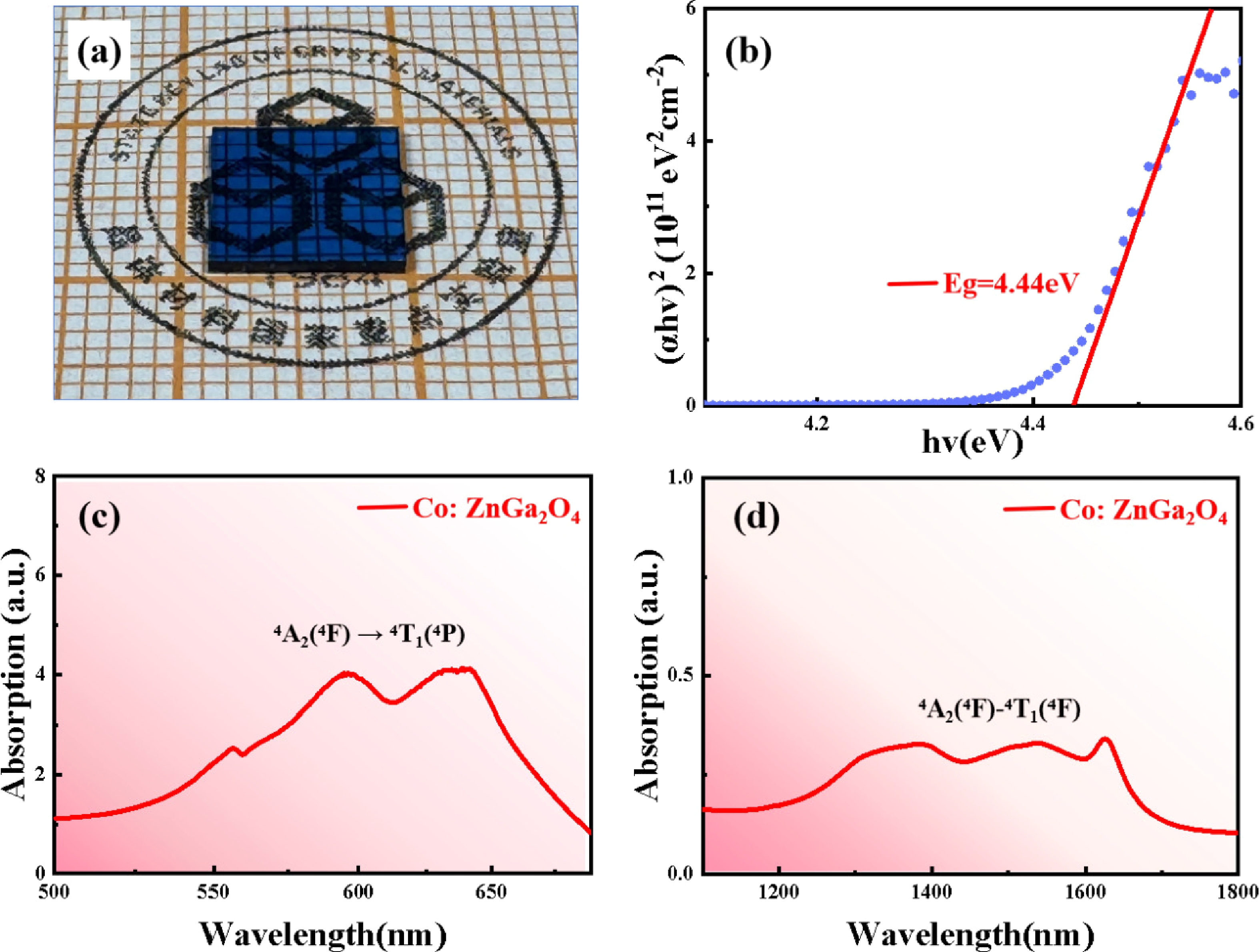
The transition of cobalt ions located at tetrahedral sites will produce strong absorption in the visible and near-infrared regions, and is expected to work in a passively Q-switched solid-state laser at the eye-safe wavelength of 1.5 µm. In this study, Co2+ ions were introduced into the wide bandgap semiconductor material ZnGa2O4, and large-sized and high-quality Co2+-doped ZnGa2O4 crystals with a volume of about 20 cm3 were grown using the vertical gradient freeze (VGF) method. Crystal structure and optical properties were analyzed using X-ray powder diffraction (XRD), X-ray photoelectron spectroscopy (XPS), and absorption spectroscopy. XRD results show that the Co2+-doped ZnGa2O4 crystal has a pure spinel phase without impurity phases and the rocking curve full width at half maximum (FWHM) is only 58 arcsec. The concentration of Co2+ in Co2+-doped ZnGa2O4 crystals was determined to be 0.2 at.% by the energy dispersive X-ray spectroscopy. The optical band gap of Co2+-doped ZnGa2O4 crystals is 4.44 eV. The optical absorption spectrum for Co2+-doped ZnGa2O4 reveals a prominent visible absorption band within 550−670 nm and a wide absorption band spanning from 1100 to 1700 nm. This suggests that the Co2+ ions have substituted the Zn2+ ions, which are typically tetrahedrally coordinated, within the lattice structure of ZnGa2O4. The visible region's absorption peak and the near-infrared broad absorption band are ascribed to the 4A2(4F) → 4T1(4P) and 4A2(4F) →4T1(4F) transitions, respectively. The optimal ground state absorption cross section was determined to be 3.07 × 10⁻¹⁹ cm2 in ZnGa2O4, a value that is comparatively large within the context of similar materials. This finding suggests that ZnGa2O4 is a promising candidate for use in near-infrared passive Q-switched solid-state lasers.
J. Semicond.
2025, 46(7): 072701 doi: 10.1088/1674-4926/24090048
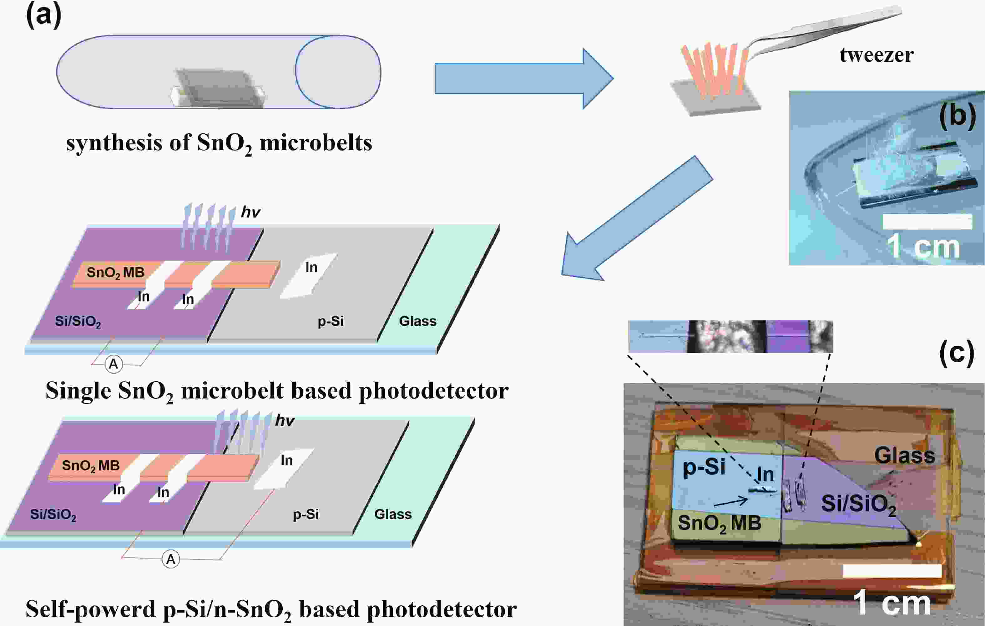
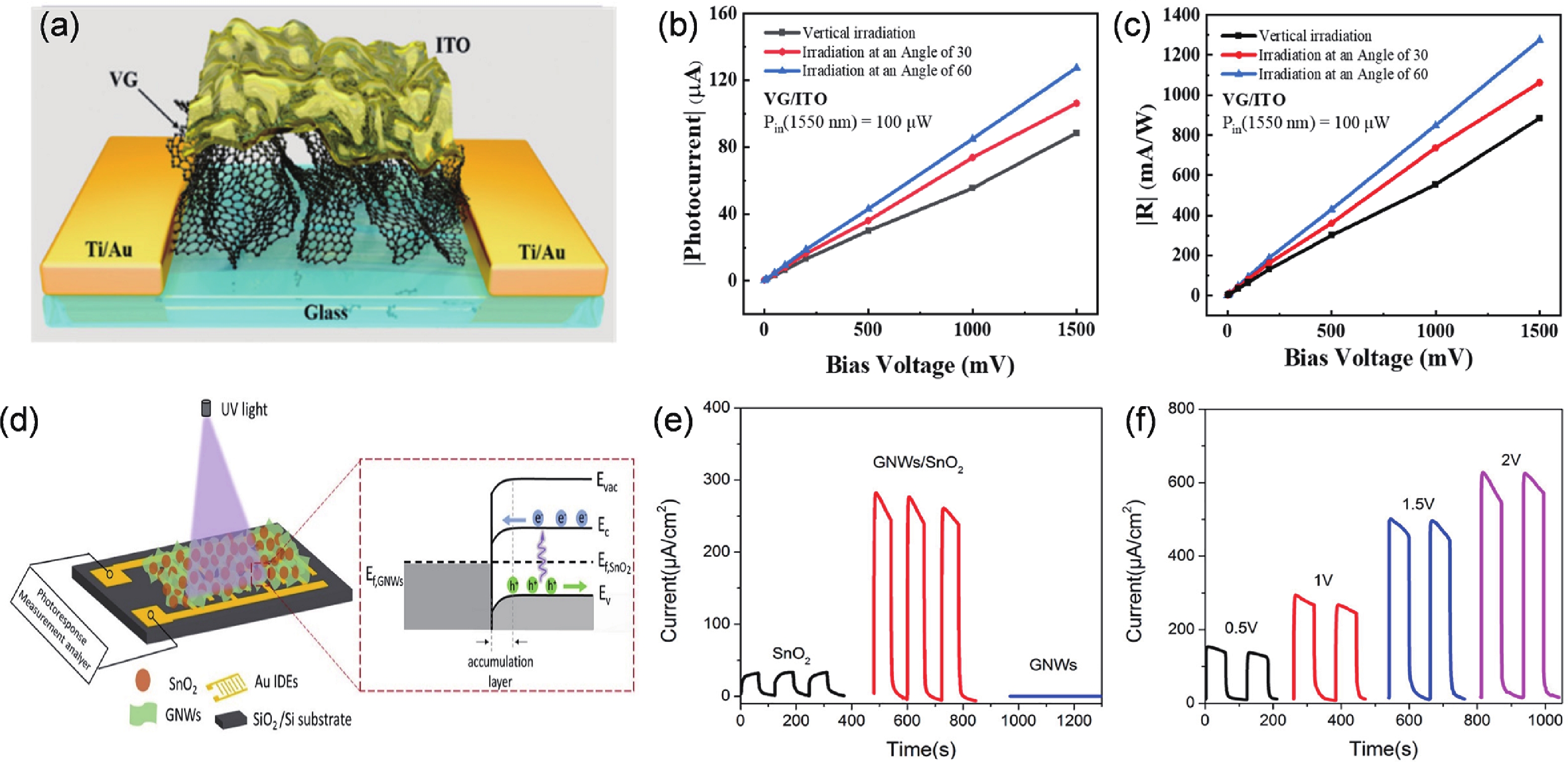
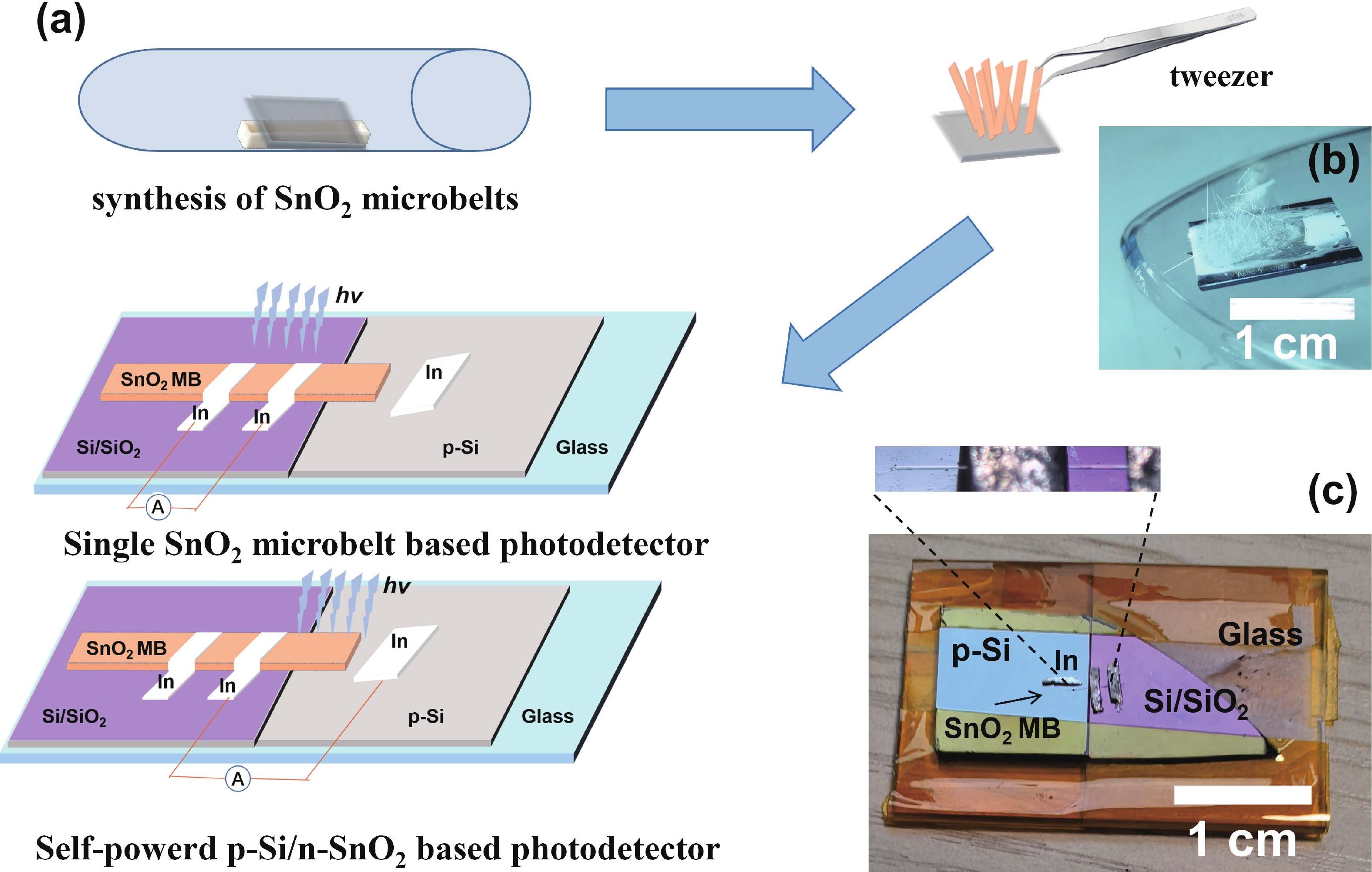
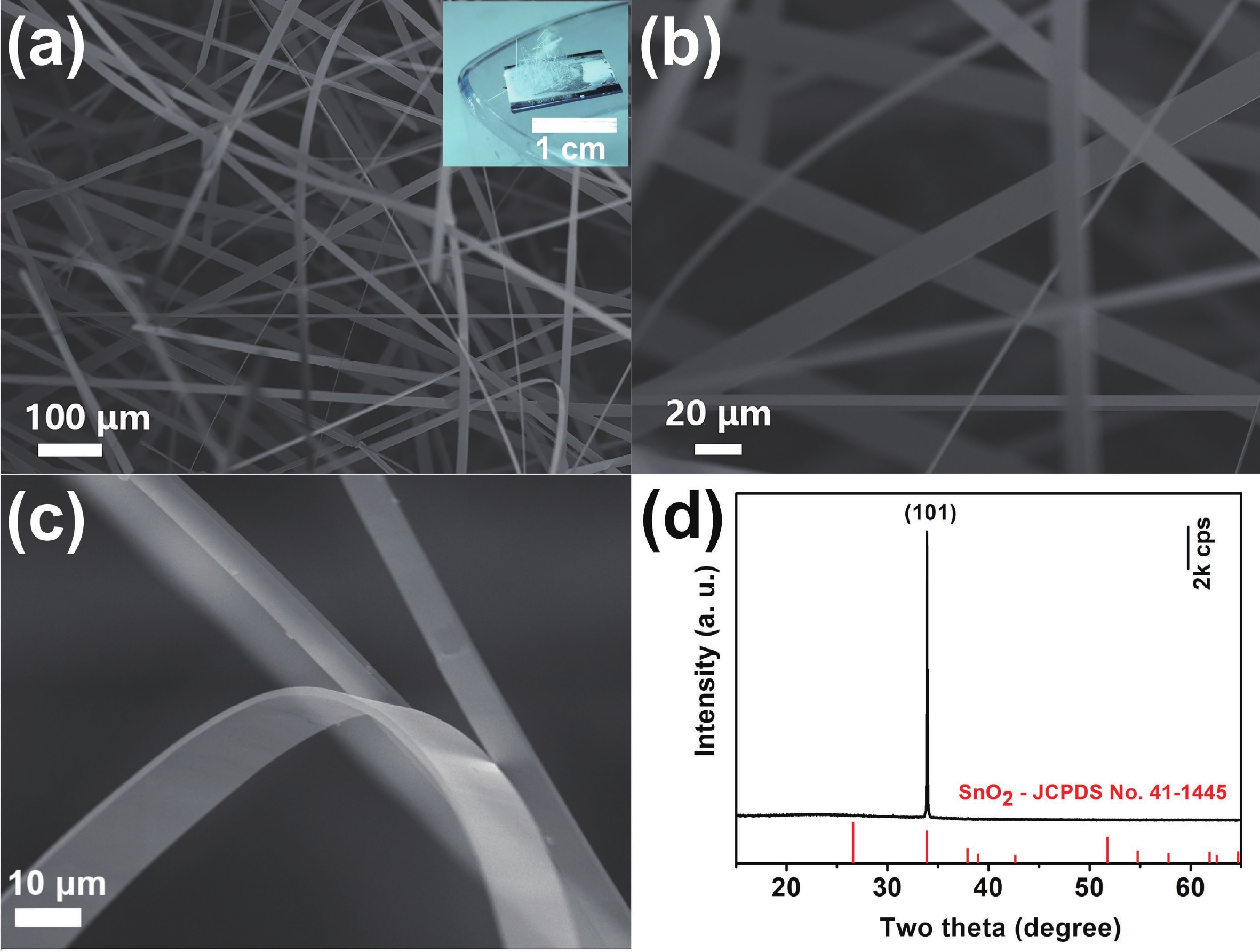
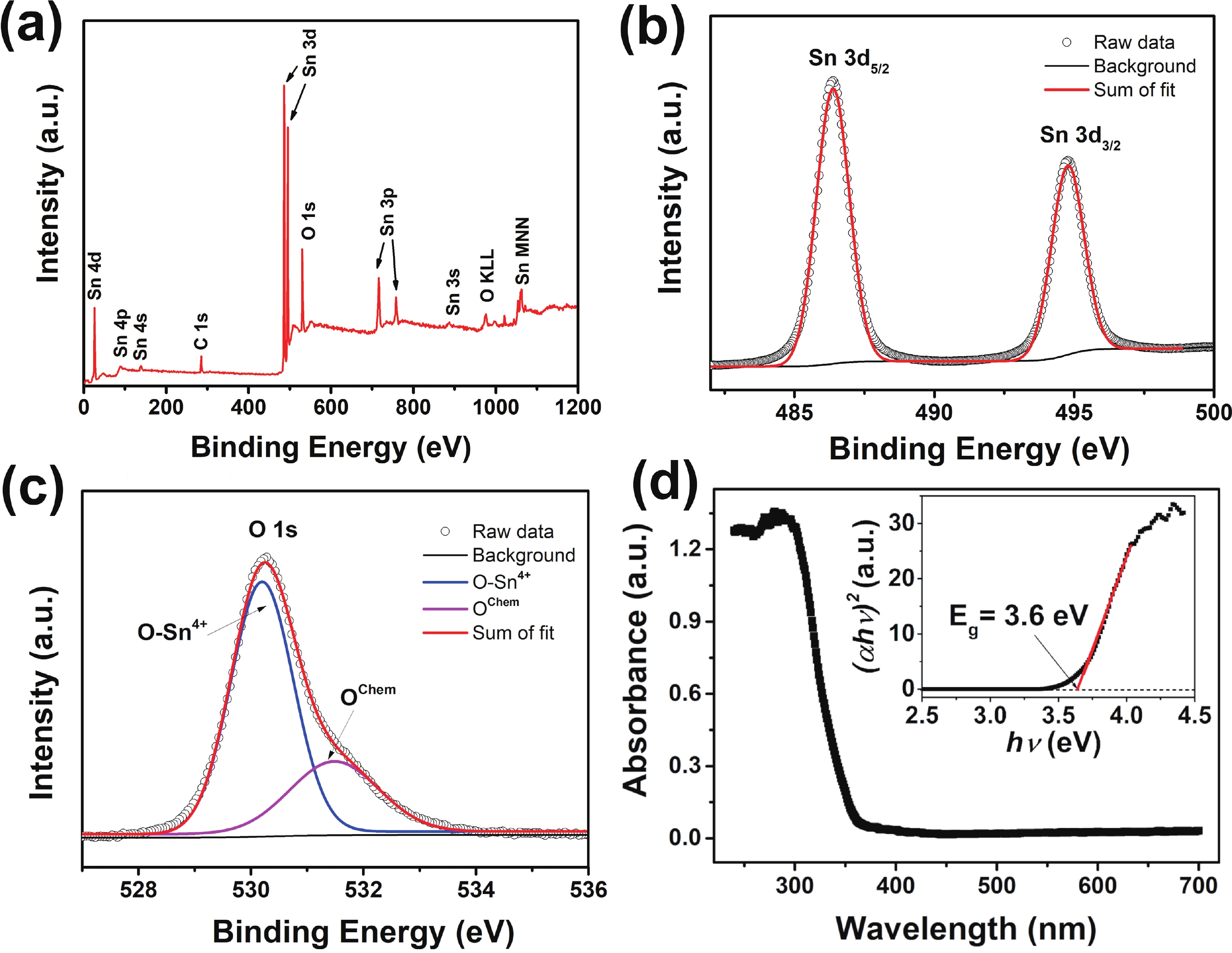
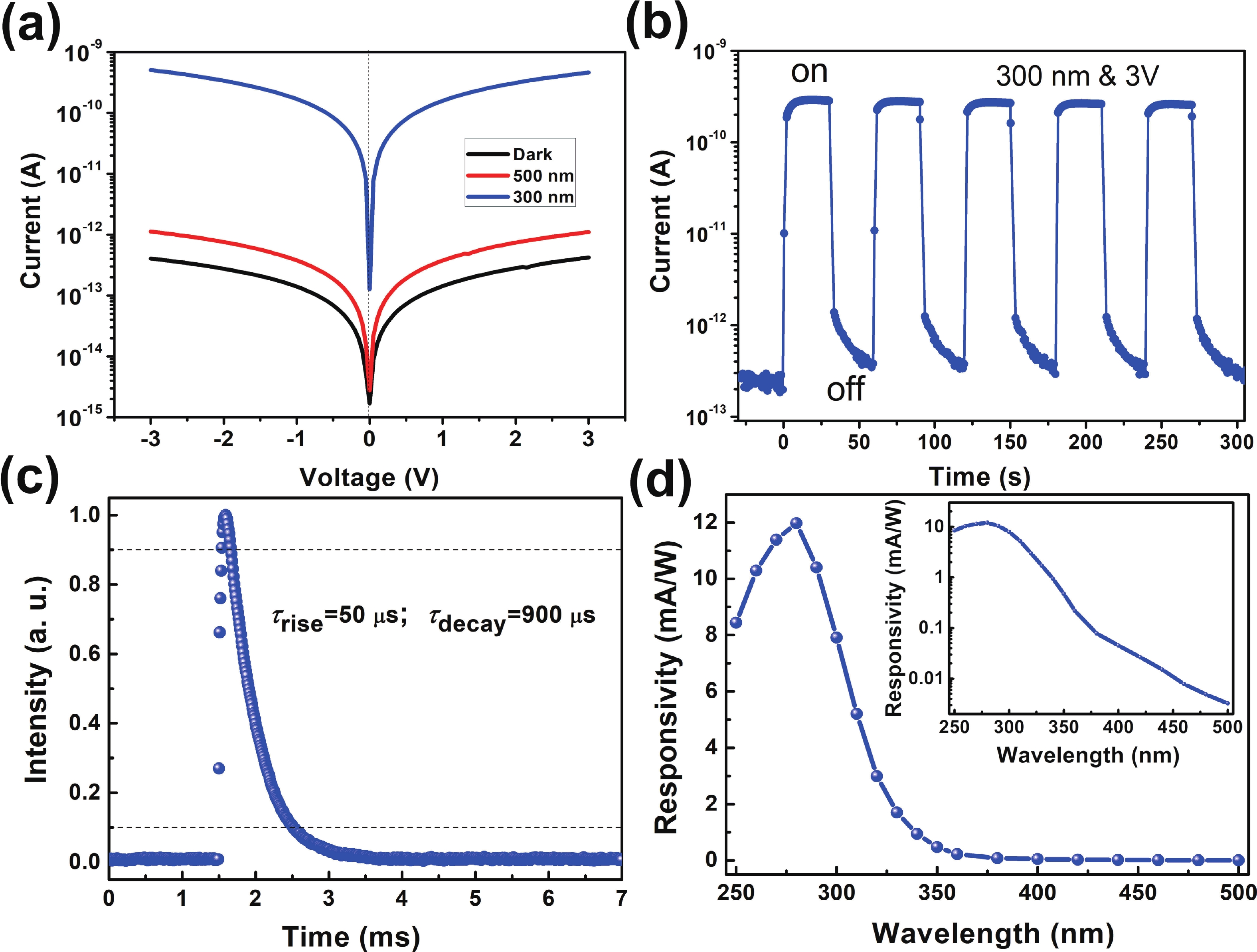
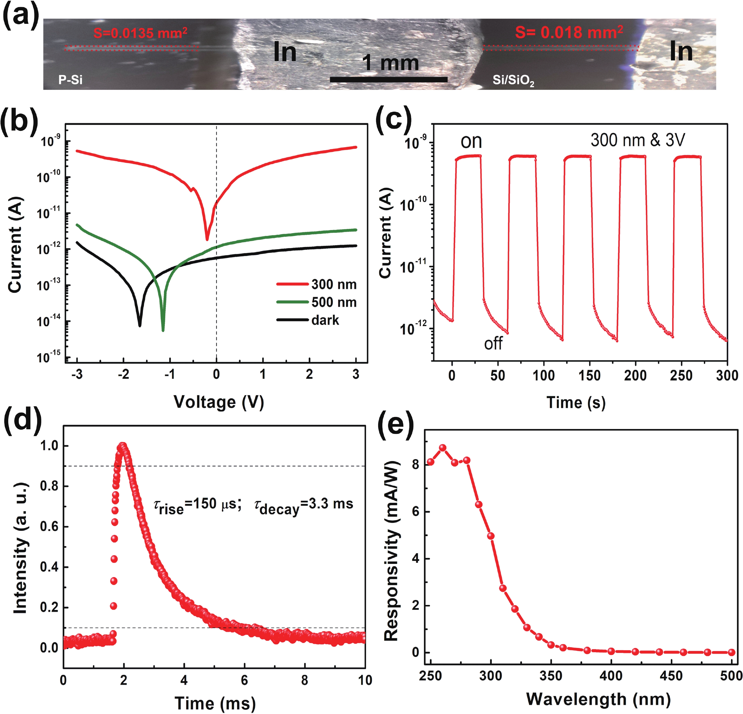
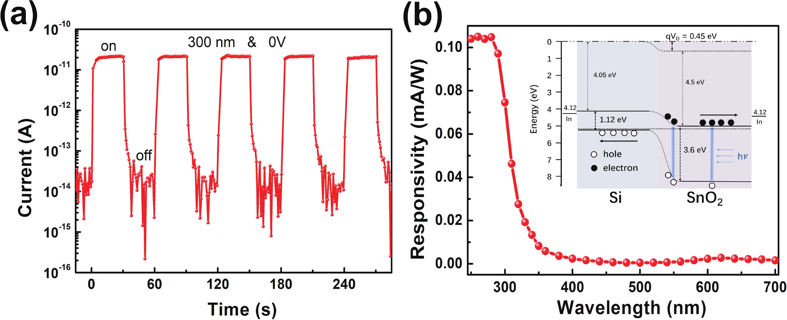
Recently, self-powered ultraviolet photodetectors (UV PDs) based on SnO2 have gained increasing interest due to its feature of working continuously without the need for external power sources. Nevertheless, the production of the majority of these existing UV PDs necessitates additional manufacturing stages or intricate processes. In this work, we present a facile, cost-effective approach for the fabrication of a self-powered UV PD based on p-Si/n-SnO2 junction. The self-powered device was achieved simply by integrating a p-Si substrate with a n-type SnO2 microbelt, which was synthesized via the chemical vapor deposition (CVD) method. The high-quality feature, coupled with the belt-like shape of the SnO2 microbelt enables the favorable contact between the n-type SnO2 and p-type silicon. The built-in electric field created at the interface endows the self-powered performance of the device. The p-Si/n-SnO2 junction photodetector demonstrated a high responsivity (0.12 mA/W), high light/dark current ratio (>103), and rapid response speed at zero bias. This method offers a practical way to develop cost-effective and high-performance self-powered UV PDs.
J. Semicond.
2025, 46(7): 072702 doi: 10.1088/1674-4926/24120033
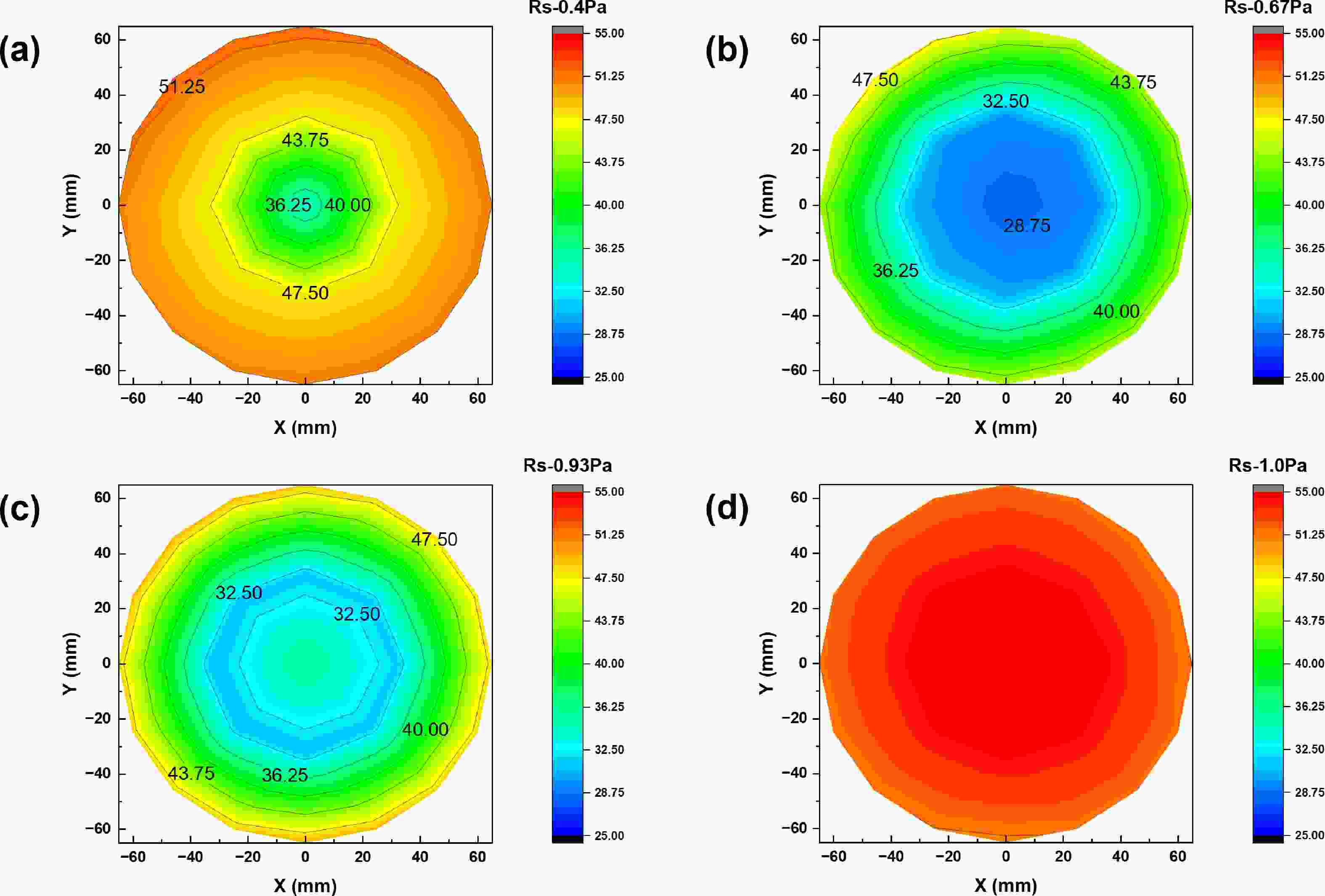
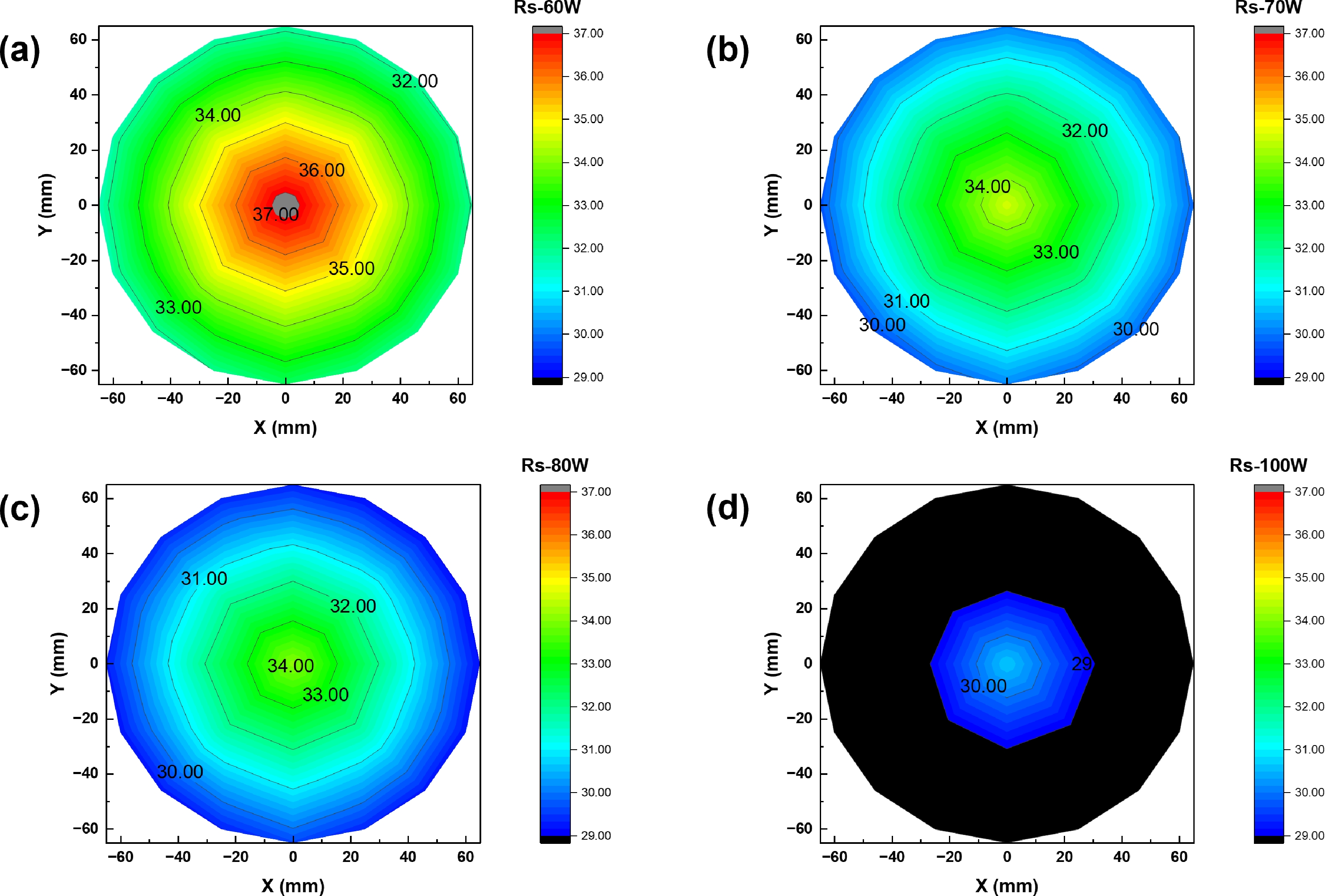
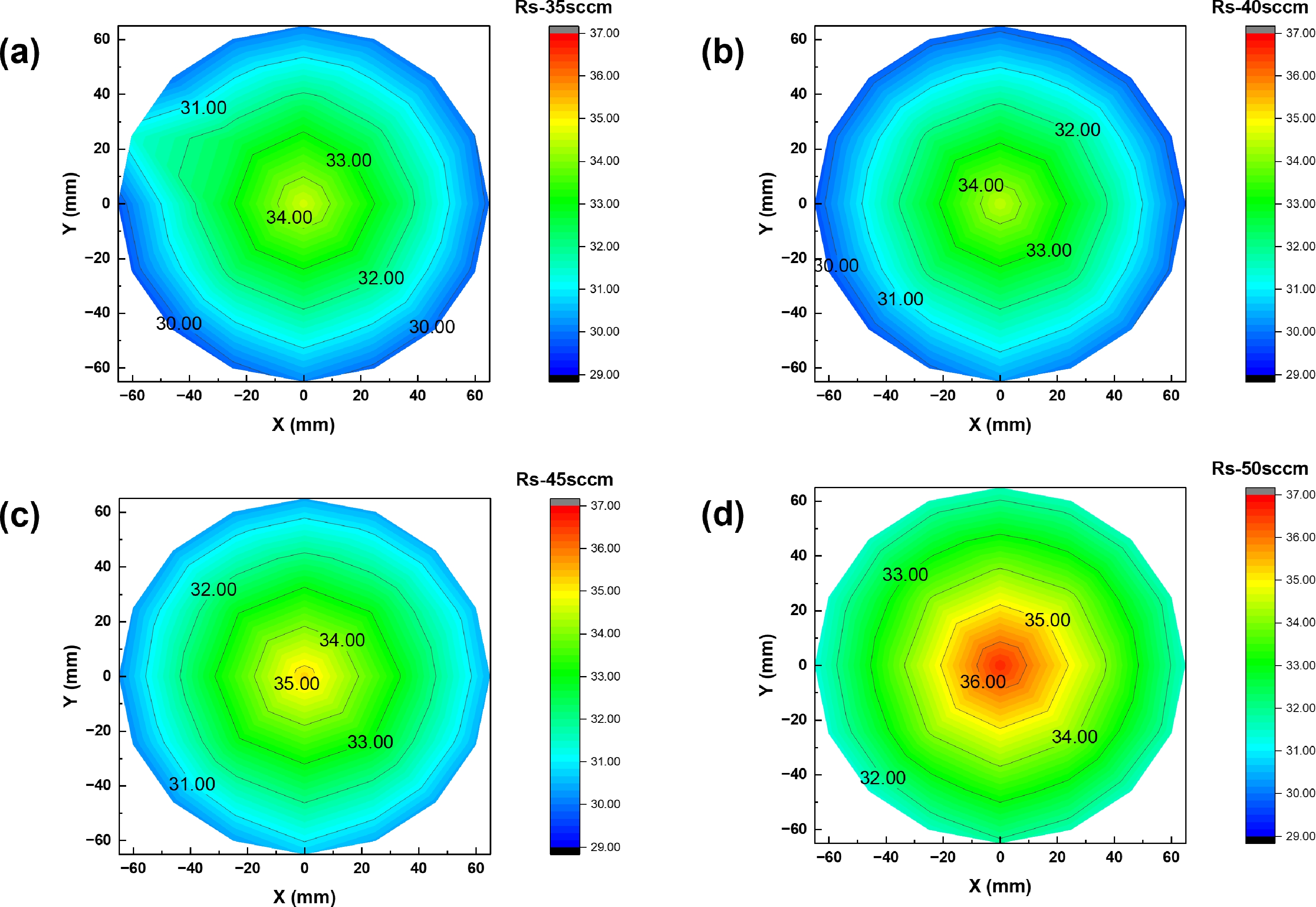
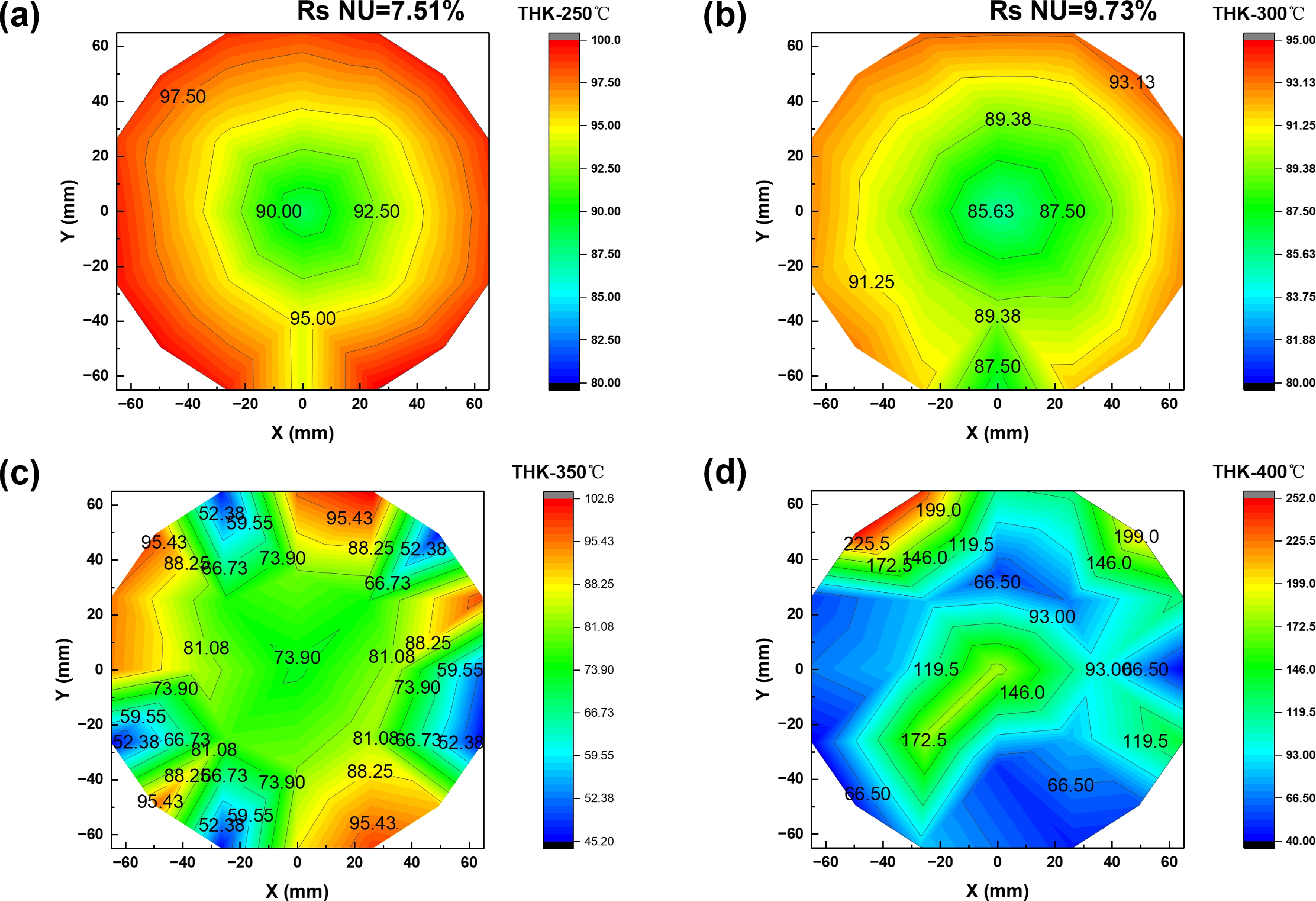
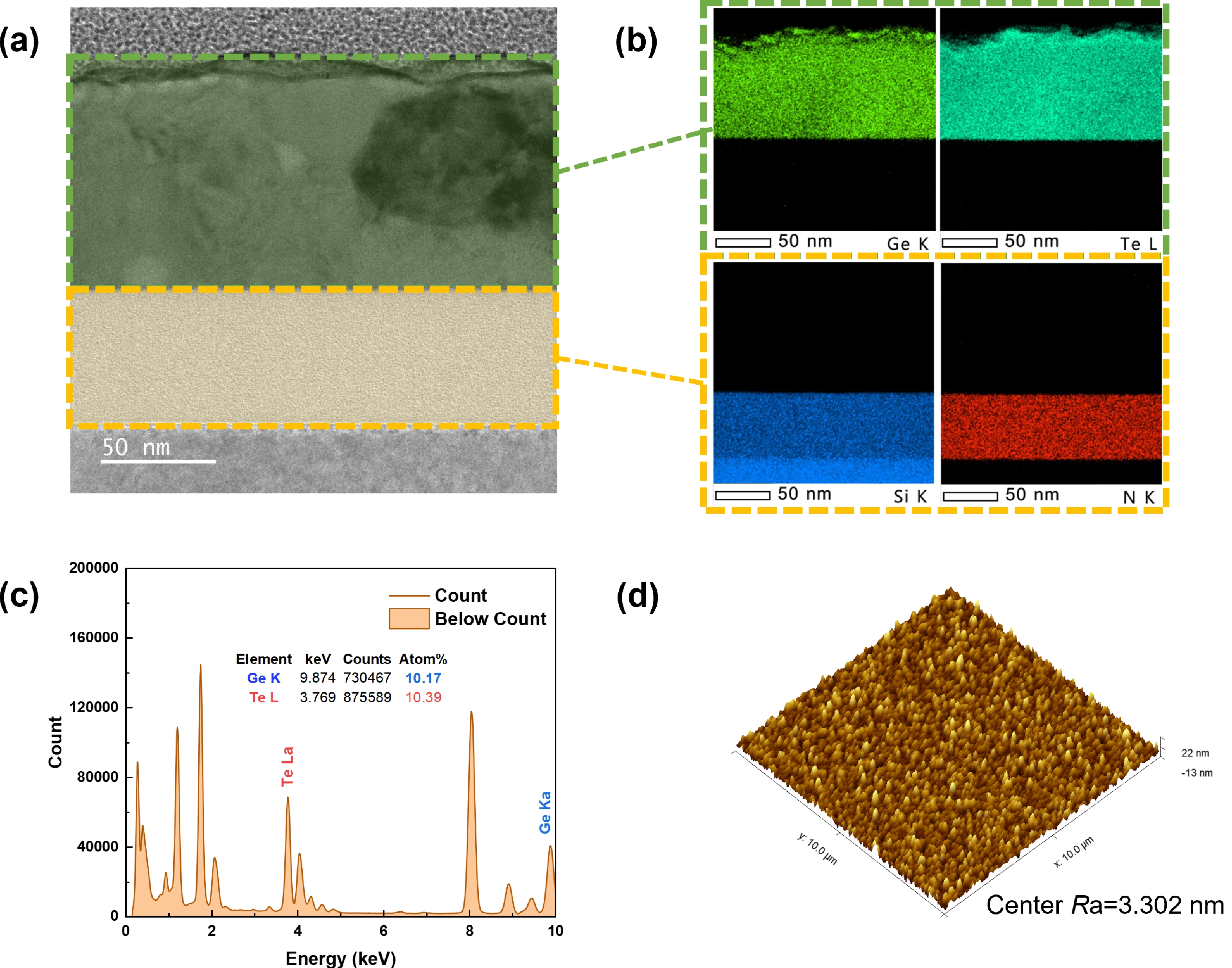
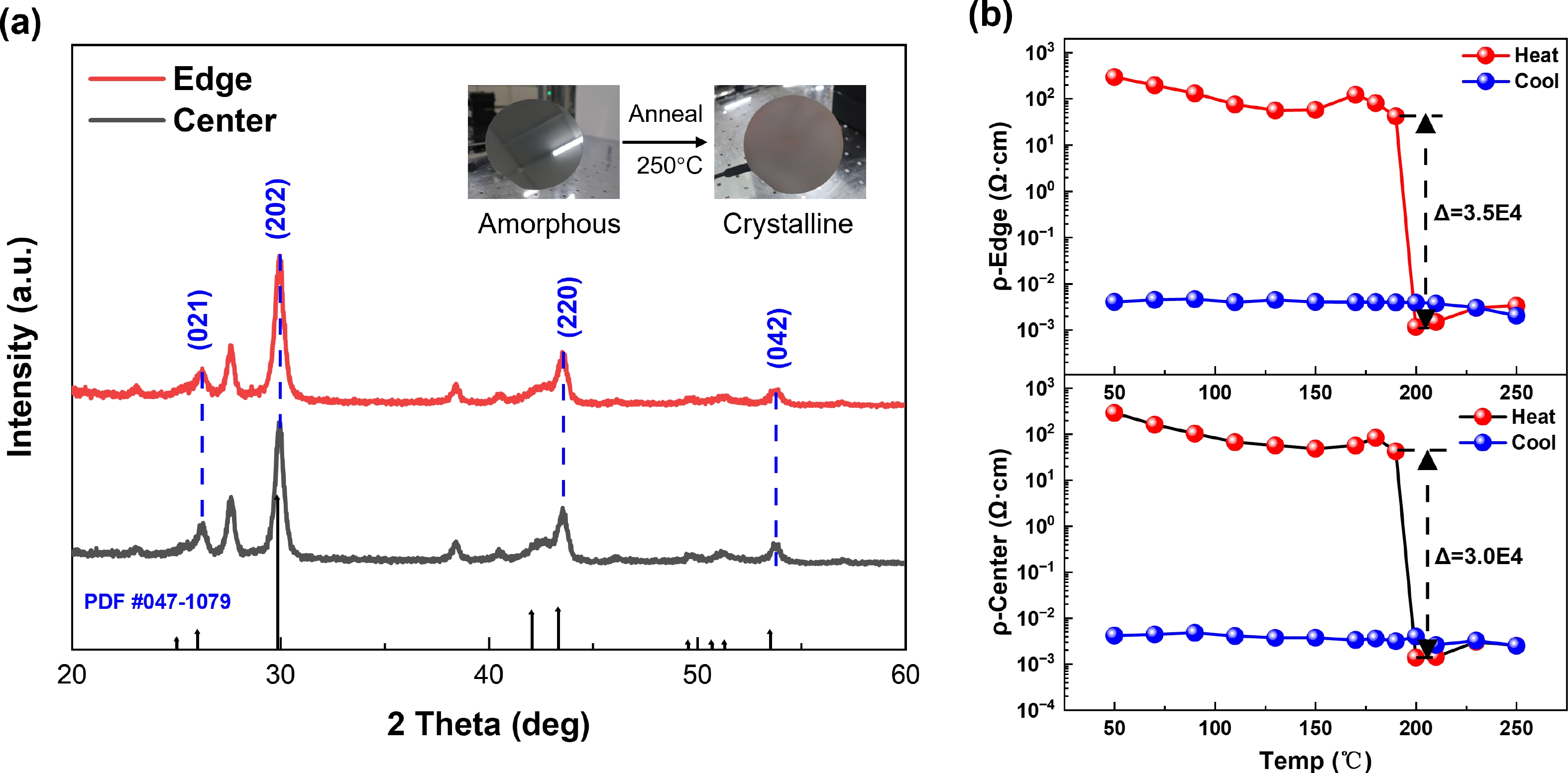
With the rapid advancement of 5G communication technology, increasingly stringent demands are placed on the performance and functionality of phase change switches. Given that RF and microwave signals exhibit characteristics of high frequency, high speed, and high precision, it is imperative for phase change switches to possess fast, accurate, and reliable switching capabilities. Moreover, wafer-level compositional homogeneity and resistivity uniformity during semiconductor manufacturing are crucial for ensuring the yield and reliability of RF switches. By controlling magnetron sputter of GeTe through from four key parameters (pressure, power, Ar flow, and post-annealing) and incorporating elemental proportional compensation in the target, we achieved effective modulation over GeTe uniformity. Finally, we successfully demonstrated the process integration of GeTe phase-change RF switches on 6-inch scaled wafers.

J. Semicond.
2025, 46(7): 072801 doi: 10.1088/1674-4926/24120010
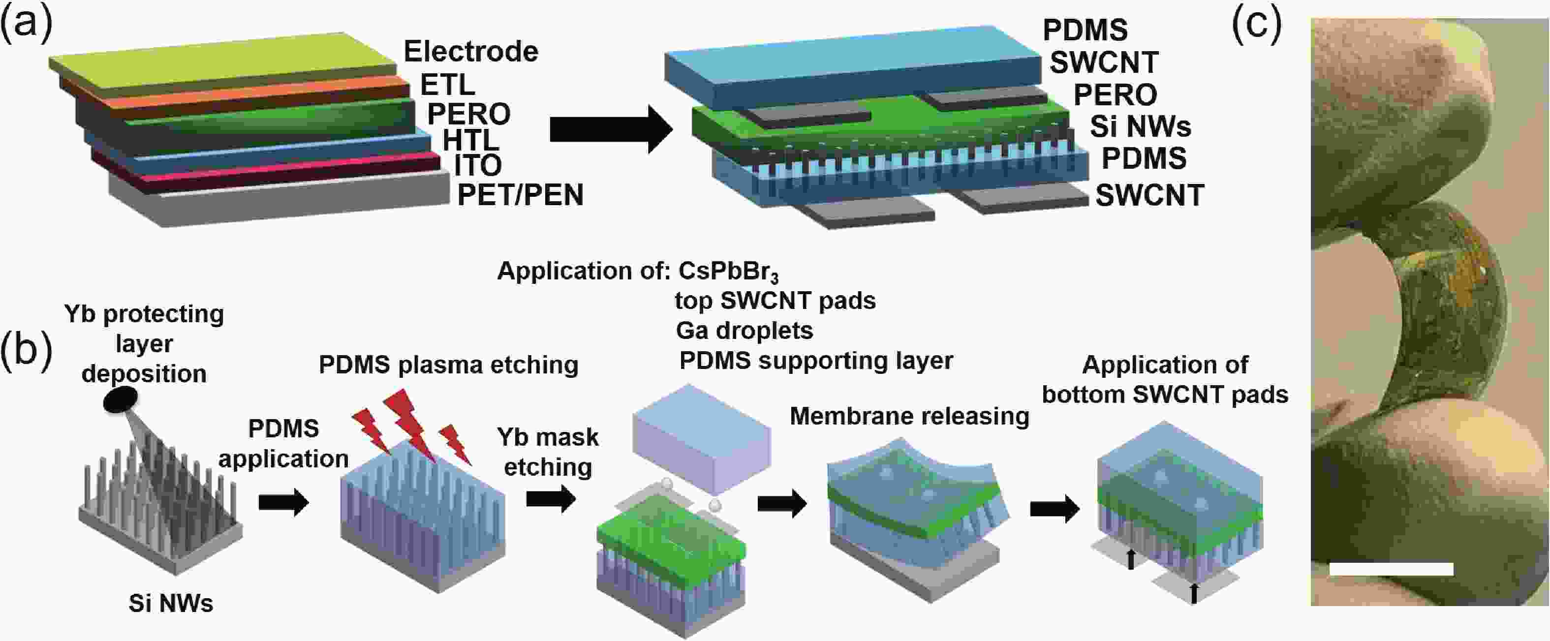
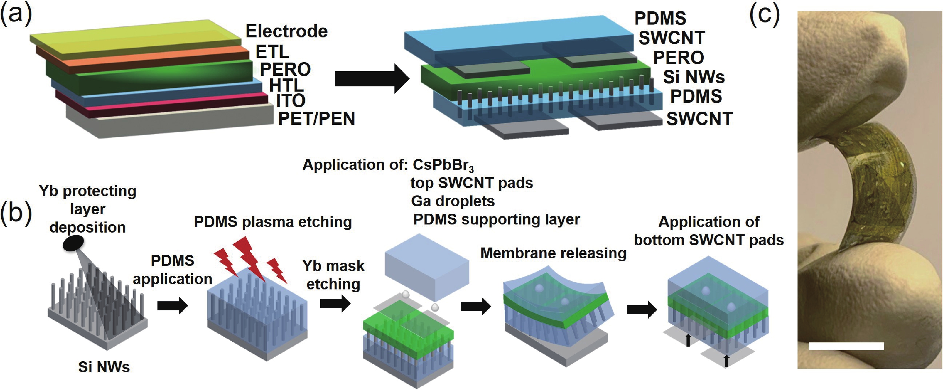
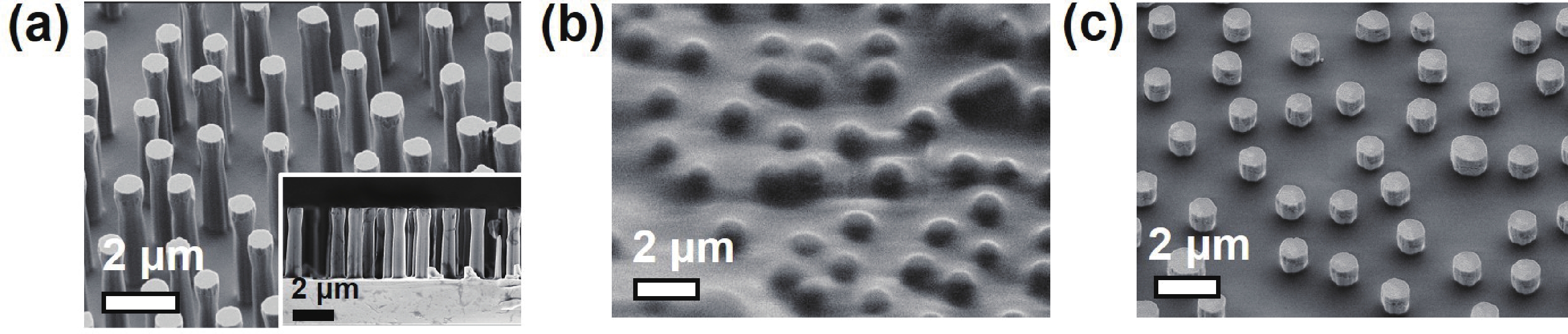
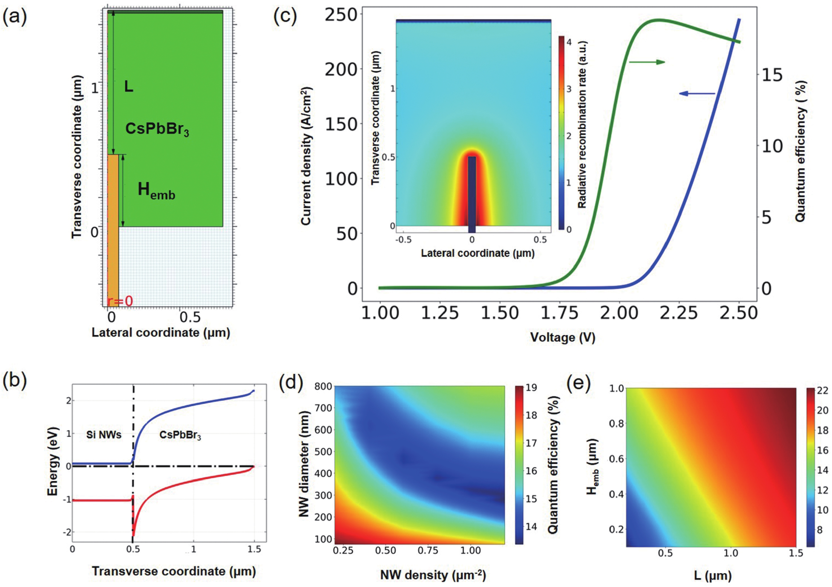
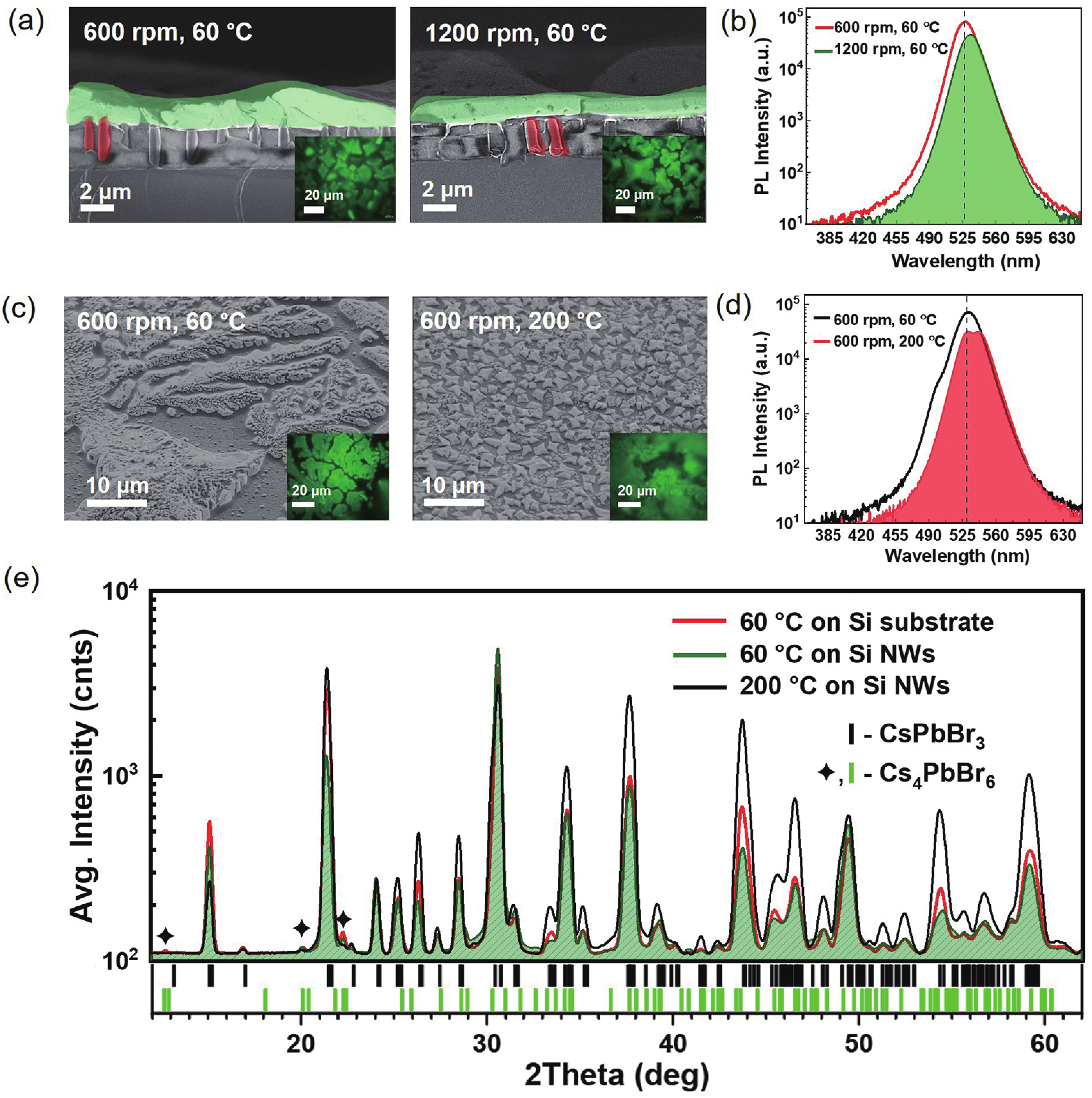
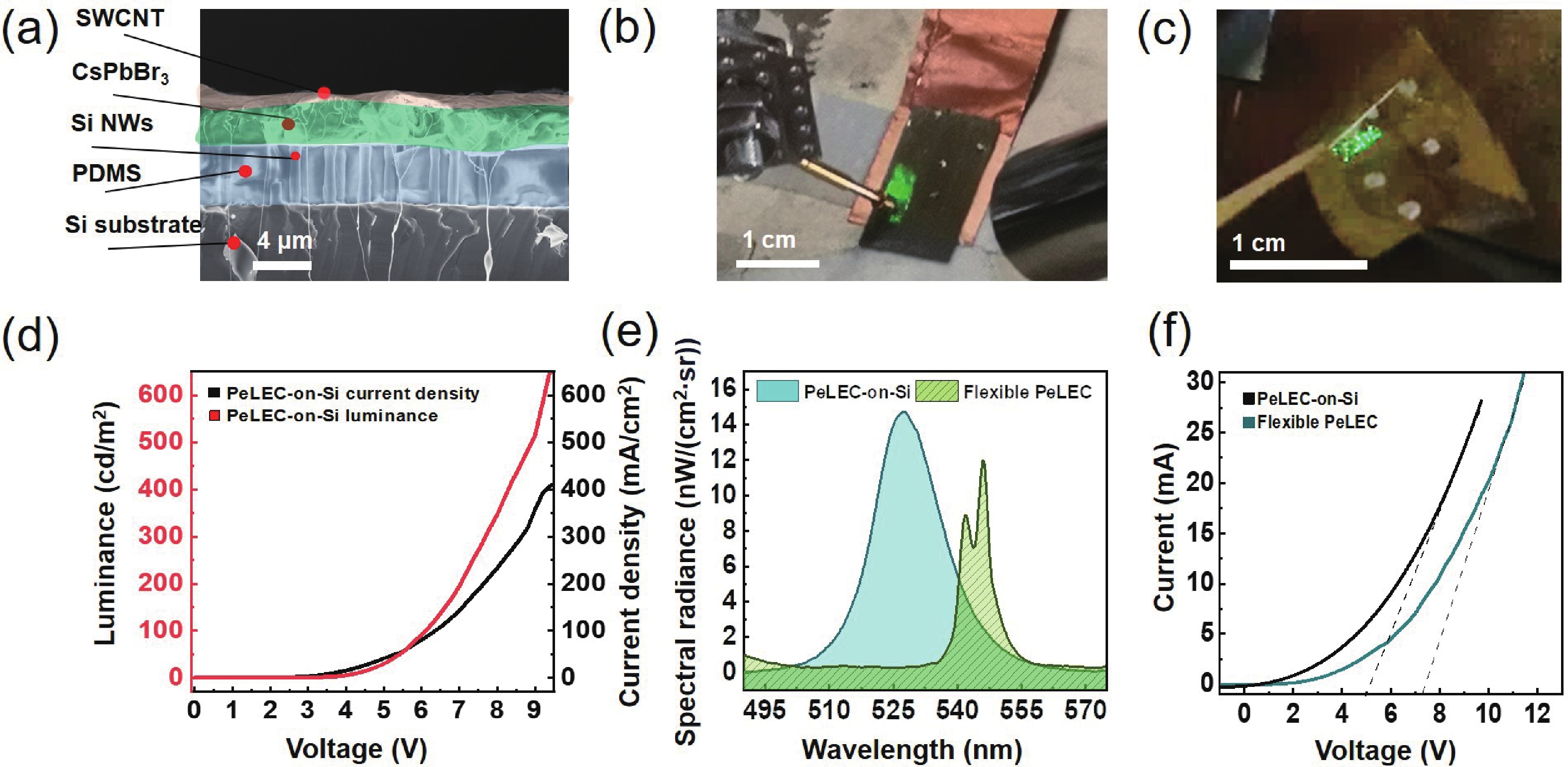
The emergence of cesium lead halide perovskite materials stable at air opened new prospects for the optoelectronic industry. In this work we present an approach to fabricating a flexible green perovskite light-emitting electrochemical cell (PeLEC) with a CsPbBr3 perovskite active layer using a highly-ordered silicon nanowire (Si NW) array as a distributed electrode integrated within a thin polydimethylsiloxane film (PDMS). Numerical simulations reveal that Si NWs-based distributed electrode aids the improvement of carrier injection into the perovskite layer with an increased thickness and, therefore, the enhancement of light-emitting performance. The X-ray diffraction study shows that the perovskite layer synthesized on the PDMS membrane with Si NWs has a similar crystal structure to the ones synthesized on planar Si wafers. We perform a comparative analysis of the light-emitting devices’ properties fabricated on rigid silicon substrates and flexible Si NW-based membranes released from substrates. Due to possible potential barriers in a flexible PeLEC between the bottom electrode (made of a network of single-walled carbon nanotube film) and Si NWs, the electroluminescence performance and I ̶ V properties of flexible devices deteriorated compared to rigid devices. The developed PeLECs pave the way for further development of inorganic flexible uniformly light-emitting devices with improved properties.