


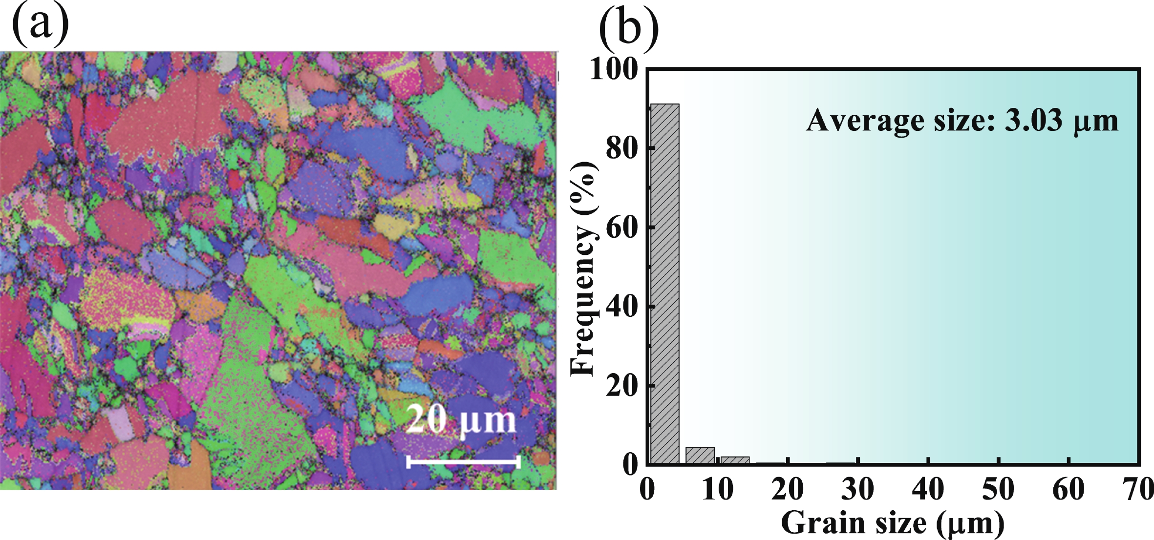
Fig. 1.
(Color online) EBSD results of (a) unintentionally doped and (b) nitrogen doped samples.
ARTICLES
Guo Li, Lei Ge, Mingsheng Xu, Jisheng Han and Xiangang Xu
Corresponding author: Lei Ge, leige@sdu.edu.cn
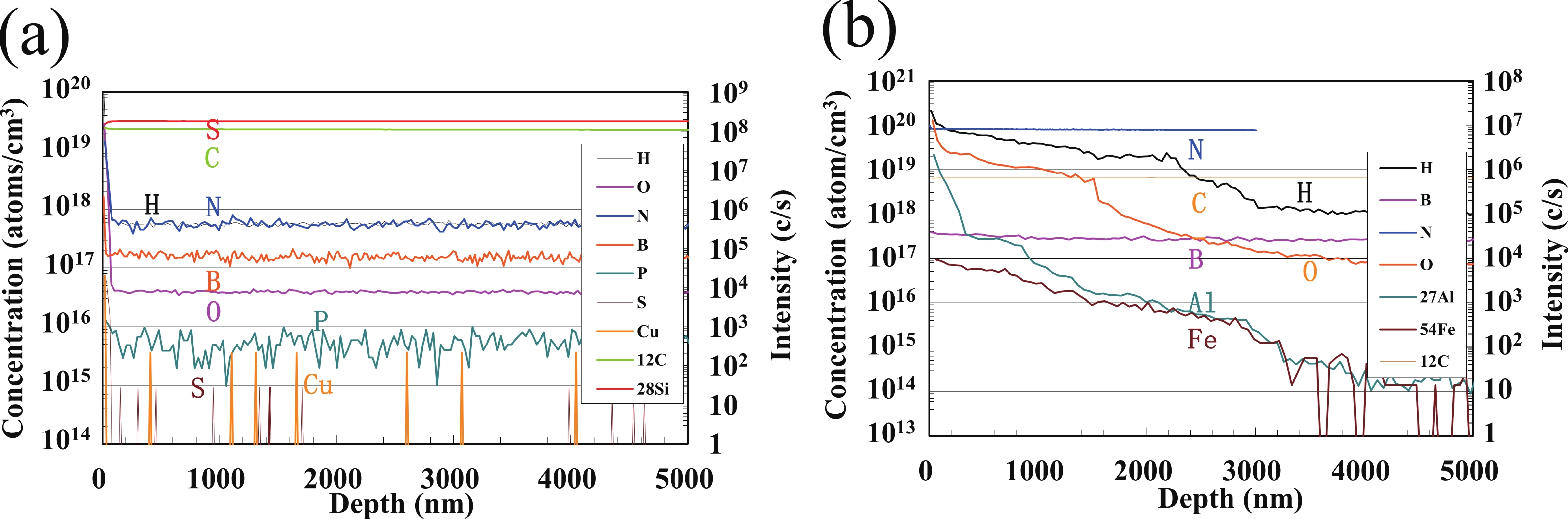
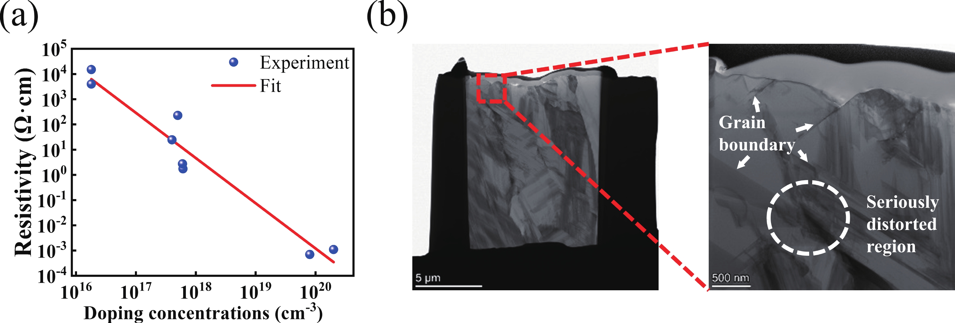
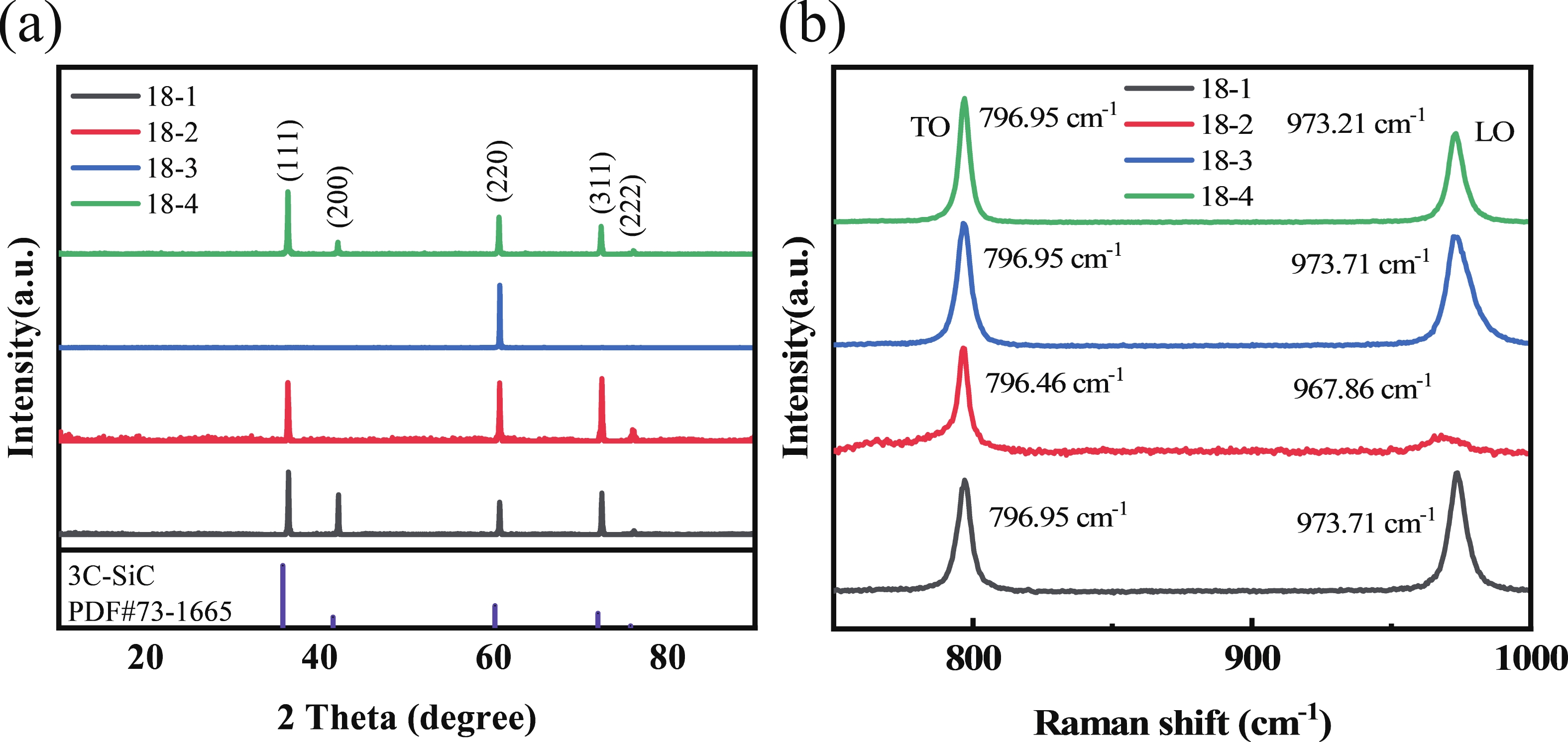
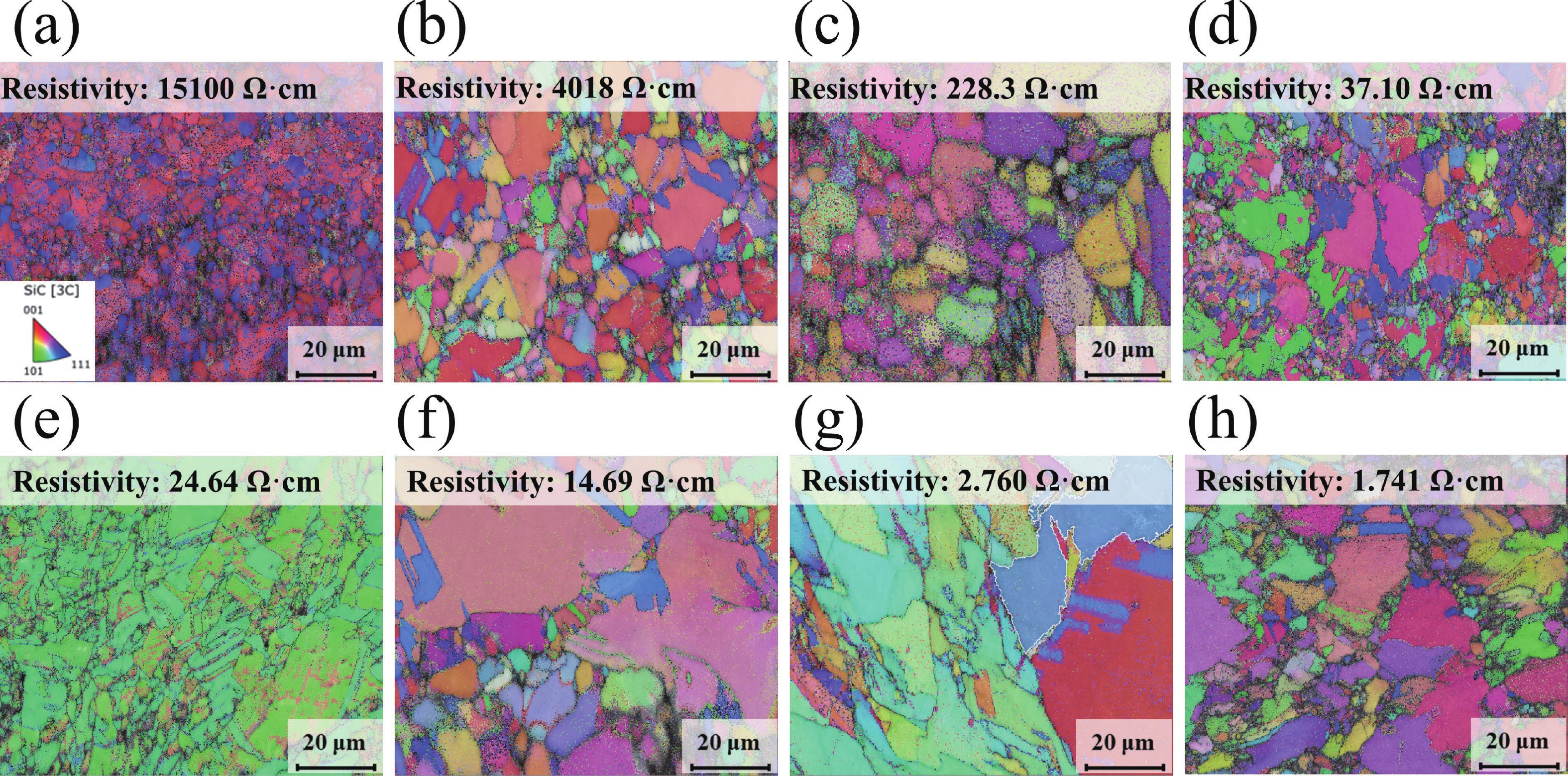
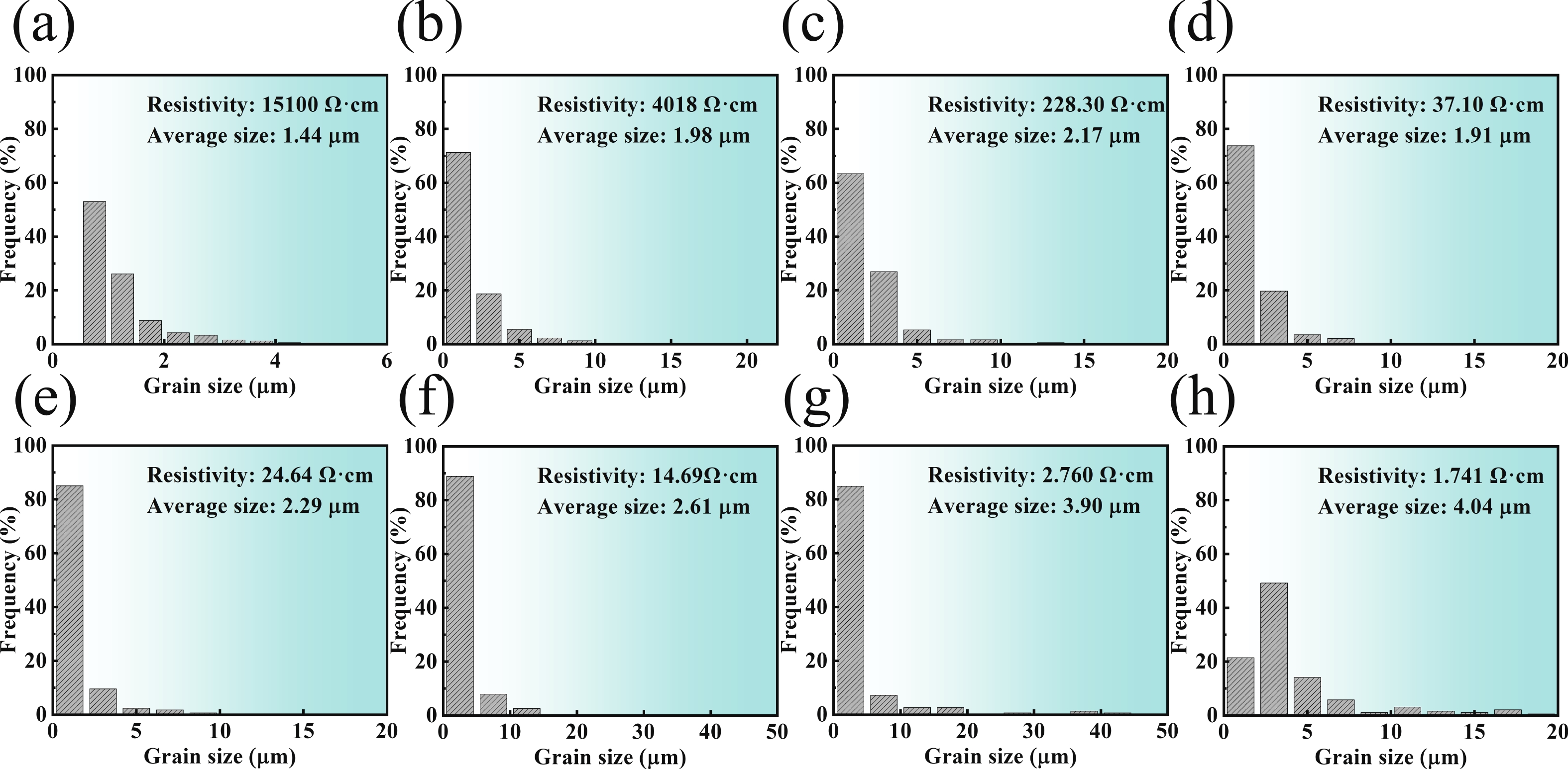
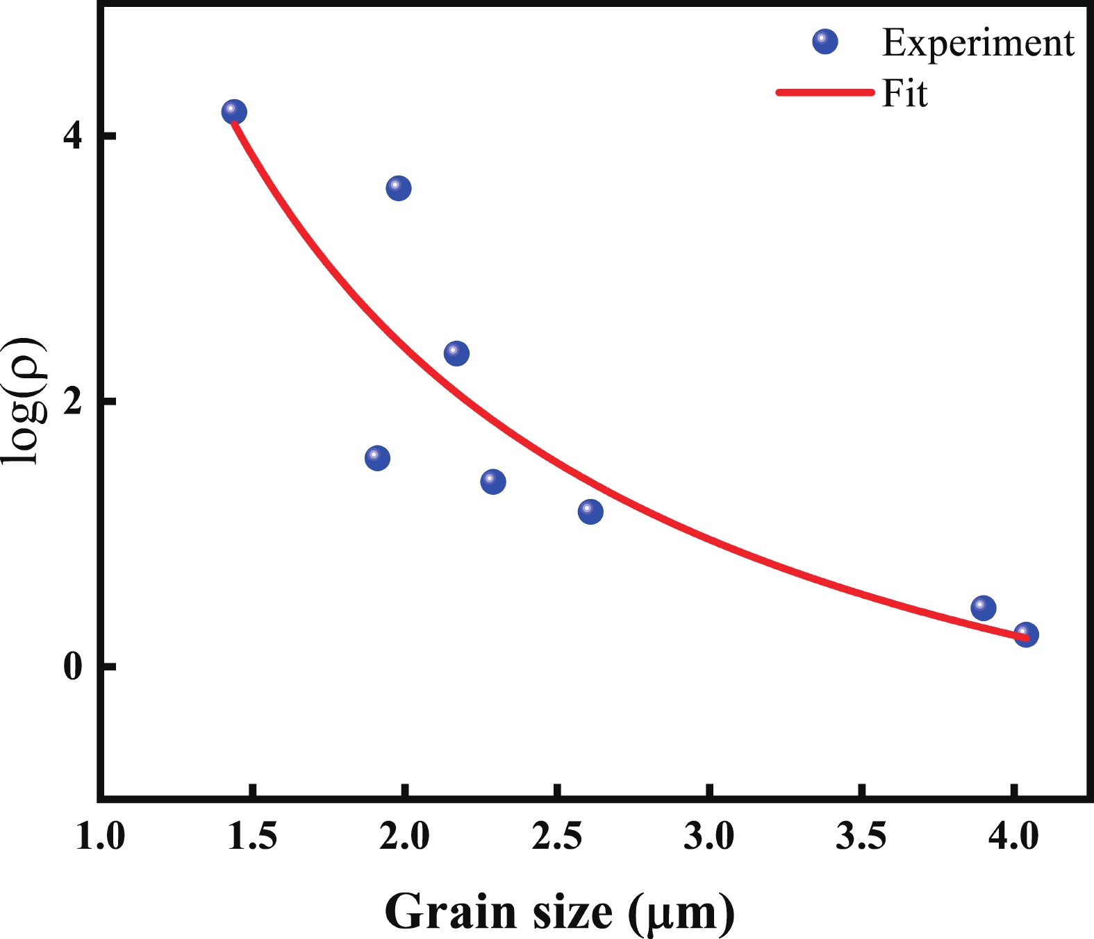
Abstract: Silicon carbide offers distinct advantages in the field of power electronic devices. However, manufacturing processes remain a significant barrier to its widespread adoption. Polycrystalline SiC is less expensive and easier to produce than single crystal. But stabilizing and controlling its performance are critical challenges that must be addressed urgently. Due to its material properties and excellent performance in applications, 3C-SiC is gaining increasing attention in research. This article presents the electrical and material properties of a series of polycrystalline 3C-SiC samples and investigates their interrelationship. The samples were examined using TEM, which confirmed their polycrystalline structure. Combined with XRD and Raman spectroscopy, the grain orientations within the samples were analyzed, and the presence of stress was verified. EBSD was employed to statistically examine the grain structure and size across samples. For samples with similar doping levels, grain size is the most influential factor in determining electrical characteristics. Further EBSD measurements reveal the relationship between resistivity and grain size as log(ρ) = −1.93 + 8.67/d. These findings provide a foundation for the quantitative control and application of polycrystalline 3C-SiC. This work offers theoretical evidence for optimizing the performance tuning of 3C-SiC ceramics and enhancing their effectiveness in electronic applications.
Keywords: 3C-SiC, polycrystalline, electrical properties, grain size
| [1] |
Itoh A, Matsunami H. Single crystal growth of SiC and electronic devices. Crit Rev Solid State Mater Sci, 1997, 22(2), 111 doi: 10.1080/10408439708241260
|
| [2] |
Fu X A, Dunning J L, Zorman C A, et al. Polycrystalline 3C-SiC thin films deposited by dual precursor LPCVD for MEMS applications. Sens Actuat A Phys, 2005, 119(1), 169 doi: 10.1016/j.sna.2004.09.009
|
| [3] |
Fissel A. Artificially layered heteropolytypic structures based on SiC polytypes: Molecular beam epitaxy, characterization and properties. Phys Rep, 2003, 379(3/4), 149 doi: 10.1016/S0370-1573(02)00632-4
|
| [4] |
Via F L, Severino A, Anzalone R, et al. From thin film to bulk 3C-SiC growth: Understanding the mechanism of defects reduction. Mater Sci Semicond Process, 2018, 78, 57 doi: 10.1016/j.mssp.2017.12.012
|
| [5] |
Bhatnagar M, Baliga B J. Comparison of 6H-SiC, 3C-SiC, and Si for power devices. IEEE Trans Electron Devices, 1993, 40(3), 645 doi: 10.1109/16.199372
|
| [6] |
Bakowski M, Schöner A, Ericsson P, et al. Development of 3C-SiC MOSFETs. J Telecommun Inf Technol, 2007, (2), 49 doi: 10.26636/jtit.2007.2.808
|
| [7] |
Ohtani N, Fujimoto T, Katsuno M, et al. Growth of large high-quality SiC single crystals. J Cryst Growth, 2002, 237, 1180 doi: 10.1016/S0022-0248(01)02153-4
|
| [8] |
Matsunami H, Kimoto T. Step-controlled epitaxial growth of SiC: High quality homoepitaxy. Mater Sci Eng R Rep, 1997, 20(3), 125 doi: 10.1016/S0927-796X(97)00005-3
|
| [9] |
Du J G, Ko W H, Mehregany M, et al. Poly-SiC capacitive pressure sensors made by wafer bonding. SENSORS, 2005 IEEE, 2005, 4 doi: 10.1109/ICSENS.2005.1597937
|
| [10] |
Zhang J C, Carraro C, Howe R T, et al. Electrical, mechanical and metal contact properties of polycrystalline 3C-SiC films for MEMS in harsh environments. Surf Coat Technol, 2007, 201(22/23), 8893 doi: 10.1016/j.surfcoat.2007.05.007
|
| [11] |
Kim K J, Lim K Y, Kim Y W, et al. Temperature dependence of electrical resistivity (4–300 K) in aluminum- and boron-doped SiC ceramics. J Am Ceram Soc, 2013, 96(8), 2525 doi: 10.1111/jace.12351
|
| [12] |
Noh S, Fu X A, Chen L, et al. A study of electrical properties and microstructure of nitrogen-doped poly-SiC films deposited by LPCVD. Sens Actuat A Phys, 2007, 136(2), 613 doi: 10.1016/j.sna.2006.12.024
|
| [13] |
Zhang J C, Howe R T, Maboudian R. Electrical characterization of n-type polycrystalline 3C-silicon carbide thin films deposited by 1, 3-disilabutane. J Electrochem Soc, 2006, 153(6), G548 doi: 10.1149/1.2188327
|
| [14] |
Asada S, Jun S D, Kimoto T. Analytical formula for temperature dependence of resistivity in p-type 4H-SiC with wide-range doping concentrations. Jpn J Appl Phys, 2018, 57(8), 088002 doi: 10.7567/JJAP.57.088002
|
| [15] |
Lu Y P, Zang X R, Du B. Investigation of the effect of the SiC particle size on the properties of the AlN–SiC composite ceramic. Mater Chem Phys, 2021, 261, 124222 doi: 10.1016/j.matchemphys.2021.124222
|
| [16] |
Xiong H F, Mao W W, Wang R, et al. Characterizations on the doping of single-crystal silicon carbide. Mater Today Phys, 2022, 29, 100906 doi: 10.1016/j.mtphys.2022.100906
|
| [17] |
Chung G S, Jeong-Hak A, Ki-Bong H. Fabrication of poly 3C-SiC thin film diodes for extreme environment applications. 2008 IEEE International Symposium on Industrial Electronics, 2008, 2576 doi: 10.1109/ISIE.2008.4676968
|
| [18] |
Zhou Z W, He W W, Zhang Z Z, et al. Characteristics of Ni-based ohmic contacts on n-type 4H-SiC using different annealing methods. Nanotechnology and Precision Engineering, 2021, 4(1), 013006 doi: 10.1063/10.0003763
|
| [19] |
Huang Y C, Wang R, Yang D R, et al. Impurities in 4H silicon carbide: Site preference, lattice distortion, solubility, and charge transition levels. J Appl Phys, 2024, 135(19), 195703 doi: 10.1063/5.0190242
|
| [20] |
Iwata H, Itoh K M. Donor and acceptor concentration dependence of the electron Hall mobility and the Hall scattering factor in n-type 4H–and 6H–SiC. J Appl Phys, 2001, 89(11), 6228 doi: 10.1063/1.1366660
|
| [21] |
Ferreira da Silva A, Pernot J, Contreras S, et al. Electrical resistivity and metal-nonmetal transition in n-type doped 4H–SiC. Phys Rev B, 2006, 74(24), 245201 doi: 10.1103/PhysRevB.74.245201
|
| [22] |
Ortiz A L, Sánchez-Bajo F, Padture N P, et al. Quantitative polytype-composition analyses of SiC using X-ray diffraction: A critical comparison between the polymorphic and the Rietveld methods. J Eur Ceram Soc, 2001, 21(9), 1237 doi: 10.1016/S0955-2219(00)00332-0
|
| [23] |
Chafai M, Jaouhari A, Torres A, et al. Raman scattering from LO phonon-plasmon coupled modes and Hall-effect in n-type silicon carbide 4H–SiC. J Eur Ceram Soc, 2001, 90(10), 5211 doi: 10.1063/1.1410884
|
| [24] |
Yokomoto K, Shioura K, Yabu M, et al. Novel characterization method for the nitrogen doping concentration in heavily nitrogen-doped 4H-SiC crystals by Raman scattering microscopy. Jpn J Appl Phys, 2020, 59(5), 051003 doi: 10.35848/1347-4065/ab8758
|
| [25] |
Anufriev R, Wu Y H, Ordonez-Miranda J, et al. Nanoscale limit of the thermal conductivity in crystalline silicon carbide membranes, nanowires, and phononic crystals. NPG Asia Mater, 2022, 14, 35 doi: 10.1038/s41427-022-00382-8
|
| [26] |
Wang J G, Huang S, Liu S, et al. EBSD characterization of the growth mechanism of SiC synthesized via direct microwave heating. Mater Charact, 2016, 114, 54 doi: 10.1016/j.matchar.2016.02.006
|
| [27] |
Bishara H, Langenohl L, Zhou X Y, et al. Decoupling the electrical resistivity contribution of grain boundaries in dilute Fe-alloyed Cu thin films. Scr Mater, 2023, 230, 115393 doi: 10.1016/j.scriptamat.2023.115393
|
| [28] |
Sun T, Yao B, Warren A P, et al. Surface and grain-boundary scattering in nanometric Cu films. Phys Rev B, 2010, 81(15), 155454 doi: 10.1103/PhysRevB.81.155454
|
| [29] |
Huang X B. A theoretical calculation for carrier concentration and resistance prediction. Phys Scr, 2020, 95(6), 065228 doi: 10.1088/1402-4896/ab6528
|
| [30] |
Bishara H, Lee S B, Brink T, et al. Understanding grain boundary electrical resistivity in Cu: The effect of boundary structure. ACS Nano, 2021, 15(10), 16607 doi: 10.1021/acsnano.1c06367
|
| [31] |
Bakonyi I, Isnaini V A, Kolonits T, et al. The specific grain-boundary electrical resistivity of Ni. Philos Mag, 2019, 99(9), 1139 doi: 10.1080/14786435.2019.1580399
|


Article views: 1185 Times PDF downloads: 175 Times Cited by: 0 Times
Received: 14 February 2025 Revised: 08 March 2025 Online: Accepted Manuscript: 21 March 2025Uncorrected proof: 16 April 2025Published: 01 August 2025
| Citation: |
Guo Li, Lei Ge, Mingsheng Xu, Jisheng Han, Xiangang Xu. Effect of grain size on the resistivity of polycrystalline 3C-SiC[J]. Journal of Semiconductors, 2025, 46(8): 082502. doi: 10.1088/1674-4926/25020018
****
G Li, L Ge, M S Xu, J S Han, and X G Xu, Effect of grain size on the resistivity of polycrystalline 3C-SiC[J]. J. Semicond., 2025, 46(8), 082502 doi: 10.1088/1674-4926/25020018

|
 Guo Li got his bachelor’s degree in 2018 and master’s degree in 2021 from Shandong University. Now he is a doctoral student at Shandong University under the supervision of Prof. Jisheng Han and Prof. Mingsheng Xu. His research focuses on the characterization SiC materials, fabracation and process of SiC device
 Lei Ge received his bachelor’s degree in 2018 and doctor’s degree in 2023 from Shandong University. He is cerrently a postdoctoral fellow at Shandong University. His research focuses on the fabrication of SiC power devices and the fabrication of diamond optoelectronic devices
| [1] |
Itoh A, Matsunami H. Single crystal growth of SiC and electronic devices. Crit Rev Solid State Mater Sci, 1997, 22(2), 111 doi: 10.1080/10408439708241260
|
| [2] |
Fu X A, Dunning J L, Zorman C A, et al. Polycrystalline 3C-SiC thin films deposited by dual precursor LPCVD for MEMS applications. Sens Actuat A Phys, 2005, 119(1), 169 doi: 10.1016/j.sna.2004.09.009
|
| [3] |
Fissel A. Artificially layered heteropolytypic structures based on SiC polytypes: Molecular beam epitaxy, characterization and properties. Phys Rep, 2003, 379(3/4), 149 doi: 10.1016/S0370-1573(02)00632-4
|
| [4] |
Via F L, Severino A, Anzalone R, et al. From thin film to bulk 3C-SiC growth: Understanding the mechanism of defects reduction. Mater Sci Semicond Process, 2018, 78, 57 doi: 10.1016/j.mssp.2017.12.012
|
| [5] |
Bhatnagar M, Baliga B J. Comparison of 6H-SiC, 3C-SiC, and Si for power devices. IEEE Trans Electron Devices, 1993, 40(3), 645 doi: 10.1109/16.199372
|
| [6] |
Bakowski M, Schöner A, Ericsson P, et al. Development of 3C-SiC MOSFETs. J Telecommun Inf Technol, 2007, (2), 49 doi: 10.26636/jtit.2007.2.808
|
| [7] |
Ohtani N, Fujimoto T, Katsuno M, et al. Growth of large high-quality SiC single crystals. J Cryst Growth, 2002, 237, 1180 doi: 10.1016/S0022-0248(01)02153-4
|
| [8] |
Matsunami H, Kimoto T. Step-controlled epitaxial growth of SiC: High quality homoepitaxy. Mater Sci Eng R Rep, 1997, 20(3), 125 doi: 10.1016/S0927-796X(97)00005-3
|
| [9] |
Du J G, Ko W H, Mehregany M, et al. Poly-SiC capacitive pressure sensors made by wafer bonding. SENSORS, 2005 IEEE, 2005, 4 doi: 10.1109/ICSENS.2005.1597937
|
| [10] |
Zhang J C, Carraro C, Howe R T, et al. Electrical, mechanical and metal contact properties of polycrystalline 3C-SiC films for MEMS in harsh environments. Surf Coat Technol, 2007, 201(22/23), 8893 doi: 10.1016/j.surfcoat.2007.05.007
|
| [11] |
Kim K J, Lim K Y, Kim Y W, et al. Temperature dependence of electrical resistivity (4–300 K) in aluminum- and boron-doped SiC ceramics. J Am Ceram Soc, 2013, 96(8), 2525 doi: 10.1111/jace.12351
|
| [12] |
Noh S, Fu X A, Chen L, et al. A study of electrical properties and microstructure of nitrogen-doped poly-SiC films deposited by LPCVD. Sens Actuat A Phys, 2007, 136(2), 613 doi: 10.1016/j.sna.2006.12.024
|
| [13] |
Zhang J C, Howe R T, Maboudian R. Electrical characterization of n-type polycrystalline 3C-silicon carbide thin films deposited by 1, 3-disilabutane. J Electrochem Soc, 2006, 153(6), G548 doi: 10.1149/1.2188327
|
| [14] |
Asada S, Jun S D, Kimoto T. Analytical formula for temperature dependence of resistivity in p-type 4H-SiC with wide-range doping concentrations. Jpn J Appl Phys, 2018, 57(8), 088002 doi: 10.7567/JJAP.57.088002
|
| [15] |
Lu Y P, Zang X R, Du B. Investigation of the effect of the SiC particle size on the properties of the AlN–SiC composite ceramic. Mater Chem Phys, 2021, 261, 124222 doi: 10.1016/j.matchemphys.2021.124222
|
| [16] |
Xiong H F, Mao W W, Wang R, et al. Characterizations on the doping of single-crystal silicon carbide. Mater Today Phys, 2022, 29, 100906 doi: 10.1016/j.mtphys.2022.100906
|
| [17] |
Chung G S, Jeong-Hak A, Ki-Bong H. Fabrication of poly 3C-SiC thin film diodes for extreme environment applications. 2008 IEEE International Symposium on Industrial Electronics, 2008, 2576 doi: 10.1109/ISIE.2008.4676968
|
| [18] |
Zhou Z W, He W W, Zhang Z Z, et al. Characteristics of Ni-based ohmic contacts on n-type 4H-SiC using different annealing methods. Nanotechnology and Precision Engineering, 2021, 4(1), 013006 doi: 10.1063/10.0003763
|
| [19] |
Huang Y C, Wang R, Yang D R, et al. Impurities in 4H silicon carbide: Site preference, lattice distortion, solubility, and charge transition levels. J Appl Phys, 2024, 135(19), 195703 doi: 10.1063/5.0190242
|
| [20] |
Iwata H, Itoh K M. Donor and acceptor concentration dependence of the electron Hall mobility and the Hall scattering factor in n-type 4H–and 6H–SiC. J Appl Phys, 2001, 89(11), 6228 doi: 10.1063/1.1366660
|
| [21] |
Ferreira da Silva A, Pernot J, Contreras S, et al. Electrical resistivity and metal-nonmetal transition in n-type doped 4H–SiC. Phys Rev B, 2006, 74(24), 245201 doi: 10.1103/PhysRevB.74.245201
|
| [22] |
Ortiz A L, Sánchez-Bajo F, Padture N P, et al. Quantitative polytype-composition analyses of SiC using X-ray diffraction: A critical comparison between the polymorphic and the Rietveld methods. J Eur Ceram Soc, 2001, 21(9), 1237 doi: 10.1016/S0955-2219(00)00332-0
|
| [23] |
Chafai M, Jaouhari A, Torres A, et al. Raman scattering from LO phonon-plasmon coupled modes and Hall-effect in n-type silicon carbide 4H–SiC. J Eur Ceram Soc, 2001, 90(10), 5211 doi: 10.1063/1.1410884
|
| [24] |
Yokomoto K, Shioura K, Yabu M, et al. Novel characterization method for the nitrogen doping concentration in heavily nitrogen-doped 4H-SiC crystals by Raman scattering microscopy. Jpn J Appl Phys, 2020, 59(5), 051003 doi: 10.35848/1347-4065/ab8758
|
| [25] |
Anufriev R, Wu Y H, Ordonez-Miranda J, et al. Nanoscale limit of the thermal conductivity in crystalline silicon carbide membranes, nanowires, and phononic crystals. NPG Asia Mater, 2022, 14, 35 doi: 10.1038/s41427-022-00382-8
|
| [26] |
Wang J G, Huang S, Liu S, et al. EBSD characterization of the growth mechanism of SiC synthesized via direct microwave heating. Mater Charact, 2016, 114, 54 doi: 10.1016/j.matchar.2016.02.006
|
| [27] |
Bishara H, Langenohl L, Zhou X Y, et al. Decoupling the electrical resistivity contribution of grain boundaries in dilute Fe-alloyed Cu thin films. Scr Mater, 2023, 230, 115393 doi: 10.1016/j.scriptamat.2023.115393
|
| [28] |
Sun T, Yao B, Warren A P, et al. Surface and grain-boundary scattering in nanometric Cu films. Phys Rev B, 2010, 81(15), 155454 doi: 10.1103/PhysRevB.81.155454
|
| [29] |
Huang X B. A theoretical calculation for carrier concentration and resistance prediction. Phys Scr, 2020, 95(6), 065228 doi: 10.1088/1402-4896/ab6528
|
| [30] |
Bishara H, Lee S B, Brink T, et al. Understanding grain boundary electrical resistivity in Cu: The effect of boundary structure. ACS Nano, 2021, 15(10), 16607 doi: 10.1021/acsnano.1c06367
|
| [31] |
Bakonyi I, Isnaini V A, Kolonits T, et al. The specific grain-boundary electrical resistivity of Ni. Philos Mag, 2019, 99(9), 1139 doi: 10.1080/14786435.2019.1580399
|

 WeChat ID
Journal of Semiconductors © 2017 All Rights Reserved 京ICP备05085259号-2

 DownLoad:

