


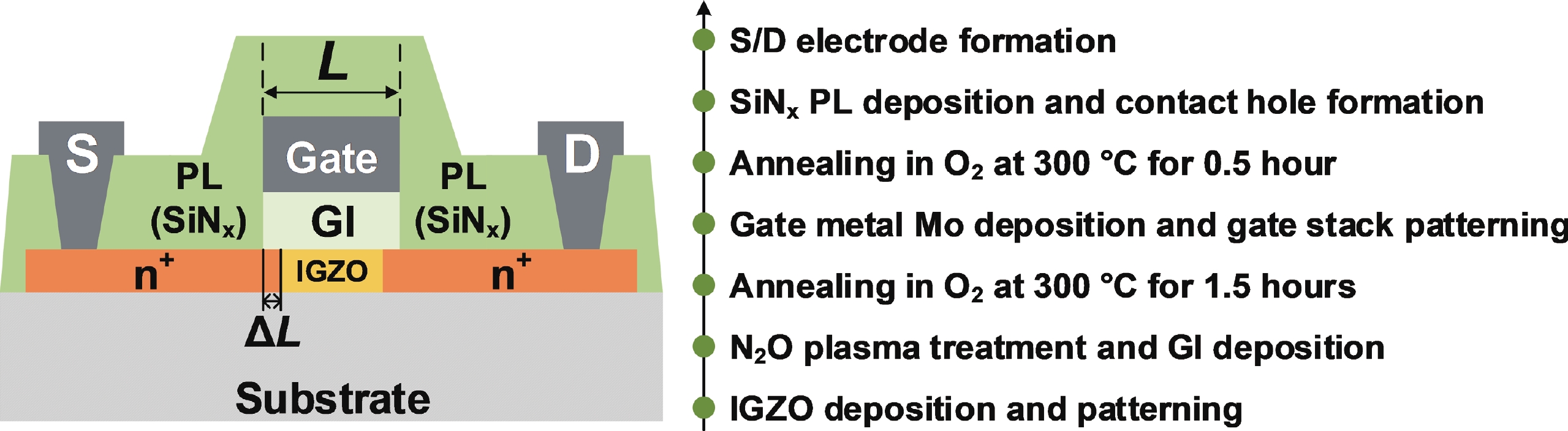
Fig. 1.
(Color online) Schematic cross-section and major processing steps of the SATG IGZO transistors.
ARTICLES
Jiye Li1, 2, Mengran Liu1, Zhendong Jiang1, Yuqing Zhang1, Hua Xu3, Lei Wang3, Congwei Liao4, Shengdong Zhang1, 2, and Lei Lu1,
Corresponding author: Shengdong Zhang, zhangsd@pku.edu.cn; Lei Lu, lulei@pku.edu.cn
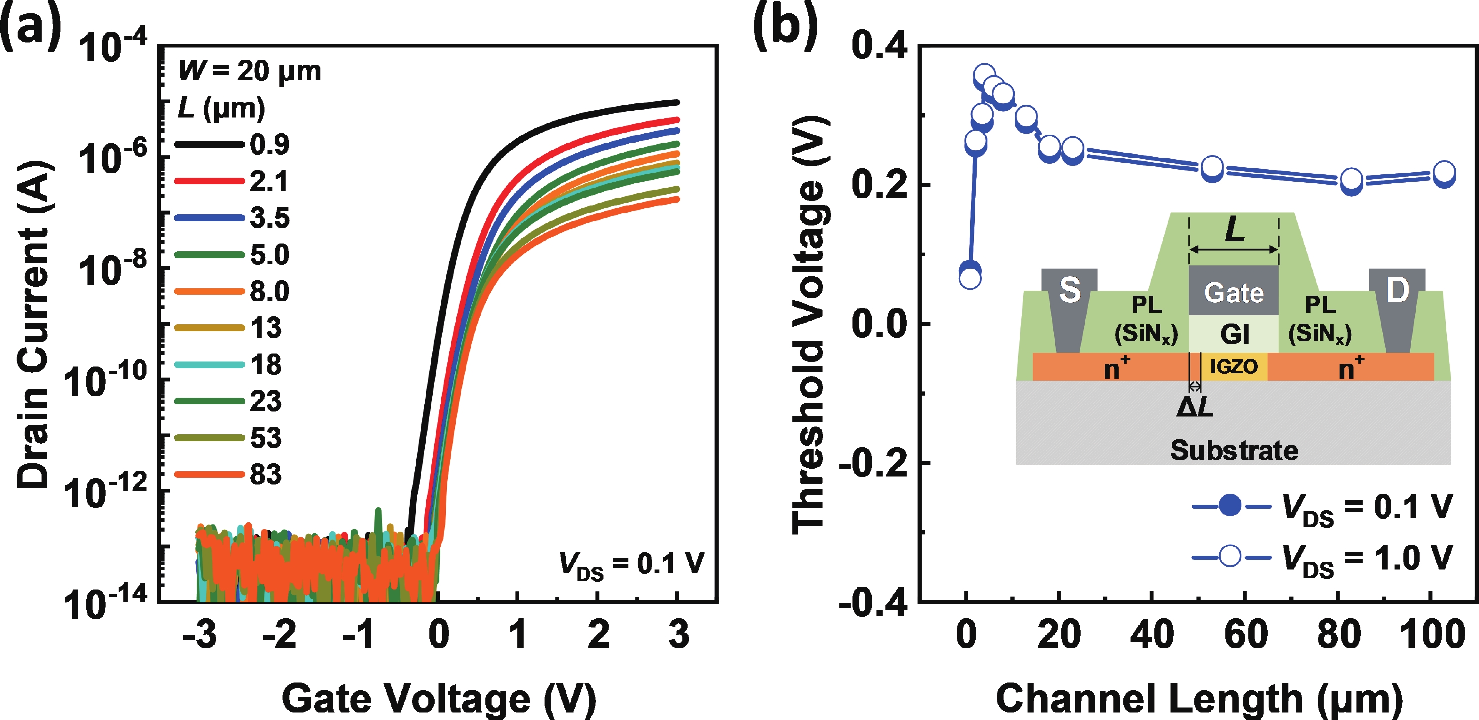
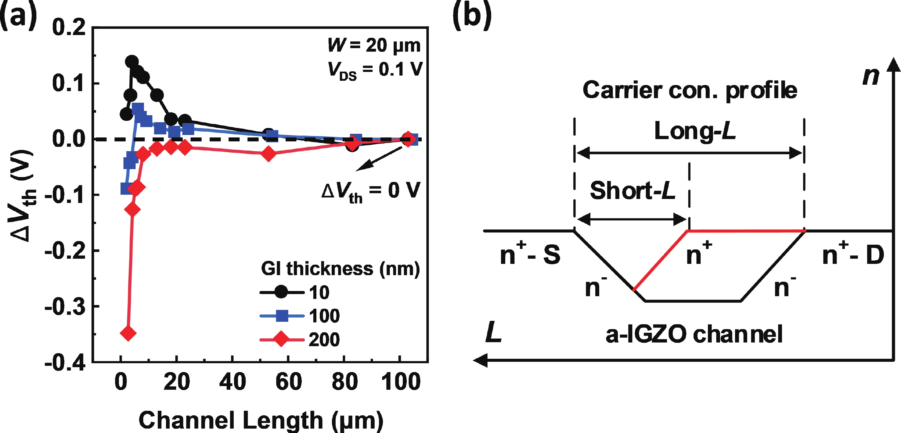
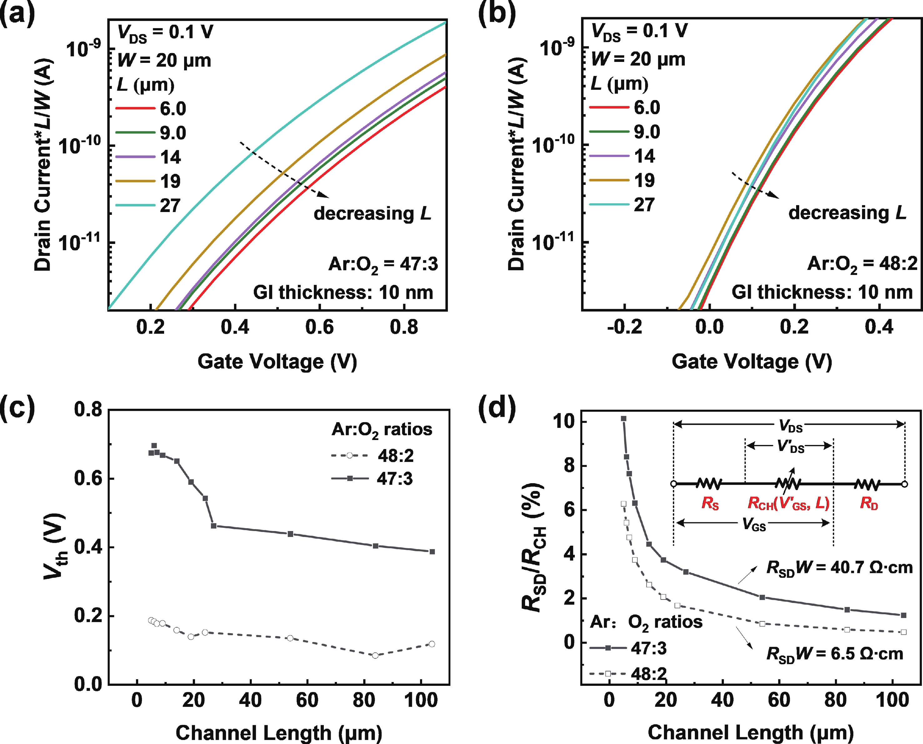
Abstract: Besides the common short-channel effect (SCE) of threshold voltage (Vth) roll-off during the channel length (L) downscaling of InGaZnO (IGZO) thin-film transistors (TFTs), an opposite Vth roll-up was reported in this work. Both roll-off and roll-up effects of Vth were comparatively investigated on IGZO transistors with varied gate insulator (GI), source/drain (S/D), and device architecture. For IGZO transistors with thinner GI, the SCE was attenuated due to the enhanced gate controllability over the variation of channel carrier concentration, while the Vth roll-up became more noteworthy. The latter was found to depend on the relative ratio of S/D series resistance (RSD) over channel resistance (RCH), as verified on transistors with different S/D. Thus, an ideal S/D engineering with small RSD but weak dopant diffusion is highly expected during the downscaling of L and GI in IGZO transistors.
Keywords: IGZO transistors, threshold voltage (Vth), roll-off, roll-up, reverse short channel effect (RSCE), short channel effect (SCE)
| [1] |
Byeon G, Jang S C, Roh T, et al. Recent progress in the development of backplane thin film transistors for information displays. J Inf Disp, 2023, 24(3), 159 doi: 10.1080/15980316.2023.2219030
|
| [2] |
Troughton J, Atkinson D. Amorphous InGaZnO and metal oxide semiconductor devices: An overview and current status. J Mater Chem C, 2019, 7(40), 12388 doi: 10.1039/C9TC03933C
|
| [3] |
Nomura K, Ohta H, Takagi A, et al. Room-temperature fabrication of transparent flexible thin-film transistors using amorphous oxide semiconductors. Nature, 2004, 432(7016), 488 doi: 10.1038/nature03090
|
| [4] |
Charnas A, Zhang Z C, Lin Z H, et al. Review-extremely thin amorphous indium oxide transistors. Adv Mater, 2024, 36(9), e2304044 doi: 10.1002/adma.202304044
|
| [5] |
Yuvaraja S, Khandelwal V, Tang X, et al. Wide bandgap semiconductor-based integrated circuits. Chip, 2023, 2(4), 100072 doi: 10.1016/j.chip.2023.100072
|
| [6] |
Wu J X, Mo F, Saraya T, et al. Monolithic integration of oxide semiconductor FET and ferroelectric capacitor enabled by Sn-doped InGaZnO for 3-D embedded RAM application. IEEE Trans Electron Devices, 2021, 68(12), 6617 doi: 10.1109/TED.2021.3111145
|
| [7] |
Kim Y S, Oh H J, Kim J, et al. Approaches for 3D integration using plasma-enhanced atomic-layer-deposited atomically-ordered InGaZnO transistors with ultra-high mobility. Small Methods, 2023, 7(10), e2300549 doi: 10.1002/smtd.202300549
|
| [8] |
Wang Z H, Zheng L K, Lin Z Y, et al. CMOS logic and capacitorless DRAM by stacked oxide semiconductor and poly-Si transistors for monolithic 3-D integration. IEEE Trans Electron Devices, 2024, 71(8), 4664 doi: 10.1109/TED.2024.3418768
|
| [9] |
Hu Q L, Gu C R, Zhu S W, et al. Capacitorless DRAM cells based on high-performance indium-tin-oxide transistors with record data retention and reduced write latency. IEEE Electron Device Lett, 2023, 44(1), 60 doi: 10.1109/LED.2022.3225263
|
| [10] |
Yan S Z, Cong Z R, Lu N D, et al. Recent progress in InGaZnO FETs for high-density 2T0C DRAM applications. Sci China Inf Sci, 2023, 66(10), 200404 doi: 10.1007/s11432-023-3802-8
|
| [11] |
Su Y B, Shi M C, Tang J S, et al. Monolithic 3-D integration of counteractive coupling IGZO/CNT hybrid 2T0C DRAM and analog RRAM-based computing-In-memory. IEEE Trans Electron Devices, 2024, 71(5), 3336 doi: 10.1109/TED.2024.3372937
|
| [12] |
Si M W, Lin Z H, Chen Z Z, et al. Scaled indium oxide transistors fabricated using atomic layer deposition. Nat Electron, 2022, 5(3), 164 doi: 10.1038/s41928-022-00718-w
|
| [13] |
Wang W H, Li K, Lan J, et al. CMOS backend-of-line compatible memory array and logic circuitries enabled by high performance atomic layer deposited ZnO thin-film transistor. Nat Commun, 2023, 14(1), 6079 doi: 10.1038/s41467-023-41868-5
|
| [14] |
Kang D H, Kang I, Ryu S H, et al. Self-aligned coplanar a-IGZO TFTs and application to high-speed circuits. IEEE Electron Device Lett, 2011, 32(10), 1385 doi: 10.1109/LED.2011.2161568
|
| [15] |
Li J Y, Zhang Y Q, Wang J L, et al. High-performance self-aligned top-gate amorphous InGaZnO TFTs with 4 nm-thick atomic-layer-deposited AlOx insulator. IEEE Electron Device Lett, 2022, 43(5), 729 doi: 10.1109/LED.2022.3160514
|
| [16] |
Chen H C, Chen J J, Zhou K J, et al. Hydrogen diffusion and threshold voltage shifts in top-gate amorphous InGaZnO thin-film transistors. IEEE Trans Electron Devices, 2020, 67(8), 3123 doi: 10.1109/TED.2020.2998101
|
| [17] |
Hong S Y, Kim H J, Kim D H, et al. Study on the lateral carrier diffusion and source-drain series resistance in self-aligned top-gate coplanar InGaZnO thin-film transistors. Sci Rep, 2019, 9(1), 6588 doi: 10.1038/s41598-019-43186-7
|
| [18] |
Kang D H, Han J U, Mativenga M, et al. Threshold voltage dependence on channel length in amorphous-indium-gallium-zinc-oxide thin-film transistors. Appl Phys Lett, 2013, 102(8), 083508 doi: 10.1063/1.4793996
|
| [19] |
Kim J, Kim D H, Cho S I, et al. Channel-shortening effect suppression of a high-mobility self-aligned oxide TFT using trench structure. IEEE Electron Device Lett, 2021, 42(12), 1798 doi: 10.1109/LED.2021.3125146
|
| [20] |
Lee J K, An S, Lee S Y. Self-aligned top-gate IGZO TFT with stepped structure for suppressing short channel effect. IEEE Electron Device Lett, 2023, 44(11), 1845 doi: 10.1109/LED.2023.3317403
|
| [21] |
Frank D J, Dennard R H, Nowak E, et al. Device scaling limits of Si MOSFETs and their application dependencies. Proc IEEE, 2001, 89(3), 259 doi: 10.1109/5.915374
|
| [22] |
Bondyopadhyay P K. Moore’s law governs the silicon revolution. Proc IEEE, 1998, 86(1), 78 doi: 10.1109/5.658761
|
| [23] |
Hanafi H I, Noble W P, Bass R S, et al. A model for anomalous short-channel behavior in submicron MOSFETs. IEEE Electron Device Lett, 1993, 14(12), 575 doi: 10.1109/55.260794
|
| [24] |
Orlowski M, Mazure C, Lau F. Submicron short channel effects due to gate reoxidation induced lateral interstitial diffusion. 1987 International Electron Devices Meeting, 1987, 632 doi: 10.1109/IEDM.1987.191507
|
| [25] |
Nishida M, Onodera H. An anomalous increase of threshold voltages with shortening the channel lengths for deeply boron-implanted N-channel MOSFET’s. IEEE Trans Electron Devices, 1981, 28(9), 1101 doi: 10.1109/T-ED.1981.20494
|
| [26] |
Kim T, Choi C H, Hur J S, et al. Progress, challenges, and opportunities in oxide semiconductor devices: A key building block for applications ranging from display backplanes to 3D integrated semiconductor chips. Adv Mater, 2023, 35(43), e2204663 doi: 10.1002/adma.202204663
|
| [27] |
Peng H, Chang B Z, Fu H S, et al. Top-gate amorphous indium-gallium-zinc-oxide thin-film transistors with magnesium metallized source/drain regions. IEEE Trans Electron Devices, 2020, 67(4), 1619 doi: 10.1109/TED.2020.2975211
|
| [28] |
Zhang Y Q, Yang H, Peng H, et al. Self-aligned top-gate amorphous InGaZnO TFTs with plasma enhanced chemical vapor deposited sub-10 nm SiO2 gate dielectric for low-voltage applications. IEEE Electron Device Lett, 2019, 40(9), 1459 doi: 10.1109/LED.2019.2931358
|
| [29] |
Robertson J, Wallace R M. High-K materials and metal gates for CMOS applications. Mater Sci Eng R Rep, 2015, 88, 1 doi: 10.1016/j.mser.2014.11.001
|
| [30] |
Ide K, Nomura K, Hosono H, et al. Electronic defects in amorphous oxide semiconductors: A review. Phys Status Solidi A, 2019, 216(5), 1800372 doi: 10.1002/pssa.201800372
|
| [31] |
Ortiz-Conde A, Garcı́a Sánchez F J, Liou J J, et al. A review of recent MOSFET threshold voltage extraction methods. Microelectron Reliab, 2002, 42(4), 583 doi: 10.1016/S0026-2714(02)00027-6
|
| [32] |
Tang H W, Dekkers H, Rassoul N, et al. Study of contact resistance components in short-channel indium-gallium-zinc-oxide transistor. IEEE Trans Electron Devices, 2024, 71(1), 567 doi: 10.1109/TED.2023.3332057
|
| [33] |
Shi Y, Tsuji M, Cho H, et al. Approach to low contact resistance formation on buried interface in oxide thin-film transistors: Utilization of palladium-mediated hydrogen pathway. ACS Nano, 2024, 18(13), 9736 doi: 10.1021/acsnano.4c02101
|
| [34] |
Song A, Hong H M, Son K S, et al. Hydrogen behavior in top gate amorphous In–Ga–Zn–O device fabrication process during gate insulator deposition and gate insulator etching. IEEE Trans Electron Devices, 2021, 68(6), 2723 doi: 10.1109/TED.2021.3074120
|
| [35] |
Zhou Y, Wang M X, Wong M. Series resistance extraction in poly-Si TFTs with channel length and mobility variations. IEEE Electron Device Lett, 2011, 32(7), 901 doi: 10.1109/LED.2011.2142391
|
| [36] |
Kim S, Park J, Kim C, et al. Source/drain formation of self-aligned top-gate amorphous GaInZnO thin-film transistors by NH3 plasma treatment. IEEE Electron Device Lett, 2009, 30(4), 374 doi: 10.1109/LED.2009.2014181
|
| [37] |
Park J, Song I, Kim S, et al. Self-aligned top-gate amorphous gallium indium zinc oxide thin film transistors. Appl Phys Lett, 2008, 93(5), 053501 doi: 10.1063/1.2966145
|
| [38] |
Jeong H Y, Lee B Y, Lee Y J, et al. Coplanar amorphous-indium-gallium-zinc-oxide thin film transistor with He plasma treated heavily doped layer. Appl Phys Lett, 2014, 104(2), 022115 doi: 10.1063/1.4862320
|
| [39] |
Yang H, Zhou X L, Fu H S, et al. Metal reaction-induced bulk-doping effect in forming conductive source-drain regions of self-aligned top-gate amorphous InGaZnO thin-film transistors. ACS Appl Mater Interfaces, 2021, 13(9), 11442 doi: 10.1021/acsami.0c21123
|
| [40] |
Li J Y, Zhang Y Q, Fu H S, et al. self-aligned top-gate amorphous In-Ga-Zn-O thin-film transistors with hafnium-induced source/drain regions. Symp Digest Tech Papers, 2023, 54(1), 580 doi: 10.1002/sdtp.16624
|
| [41] |
Chen R S, Zhou W, Zhang M, et al. Self-aligned indium–gallium–zinc oxide thin-film transistor with phosphorus-doped source/drain regions. IEEE Electron Device Lett, 2012, 33(8), 1150 doi: 10.1109/LED.2012.2201444
|
| [42] |
Ye Z, Lu L, Wong M. Zinc-oxide thin-film transistor with self-aligned source/drain regions doped with implanted boron for enhanced thermal stability. IEEE Trans Electron Devices, 2012, 59(2), 393 doi: 10.1109/TED.2011.2175398
|
| [43] |
Han K Z, Samanta S, Xu S Q, et al. High field temperature-independent field-effect mobility of amorphous indium–gallium–zinc oxide thin-film transistors: Understanding the importance of equivalent-oxide-thickness downscaling. IEEE Trans Electron Devices, 2021, 68(1), 118 doi: 10.1109/TED.2020.3035737
|
| [44] |
Gu C R, Hu Q L, Li Q J, et al. 1/f noise of short-channel indium tin oxide transistors under stress. Appl Phys Lett, 2023, 122(25), 252104 doi: 10.1063/5.0147577
|
| [45] |
Zhang J, Charnas A, Lin Z H, et al. Fluorine-passivated In2O3 thin film transistors with improved electrical performance via low-temperature CF4/N2O plasma. Appl Phys Lett, 2022, 121(17), 172101 doi: 10.1063/5.0113015
|
| [46] |
Kim D G, Choi S H, Lee W B, et al. Highly robust atomic layer deposition-indium gallium zinc oxide thin-film transistors with hybrid gate insulator fabricated via two-step atomic layer process for high-density integrated all-oxide vertical complementary metal-oxide-semiconductor applications. Small Struct, 2023, 5(2), 2300375 doi: 10.1002/sstr.202300375
|


Article views: 2087 Times PDF downloads: 583 Times Cited by: 0 Times
Received: 03 December 2024 Revised: 19 February 2025 Online: Accepted Manuscript: 17 March 2025Uncorrected proof: 14 April 2025Published: 01 August 2025
| Citation: |
Jiye Li, Mengran Liu, Zhendong Jiang, Yuqing Zhang, Hua Xu, Lei Wang, Congwei Liao, Shengdong Zhang, Lei Lu. Downscaling challenges in IGZO transistors: A study on threshold voltage roll-up and roll-off effects[J]. Journal of Semiconductors, 2025, 46(8): 082301. doi: 10.1088/1674-4926/24120005
****
J Y Li, M R Liu, Z D Jiang, Y Q Zhang, H Xu, L Wang, C W Liao, S D Zhang, and L Lu, Downscaling challenges in IGZO transistors: A study on threshold voltage roll-up and roll-off effects[J]. J. Semicond., 2025, 46(8), 082301 doi: 10.1088/1674-4926/24120005

|
 Jiye Li received his BS degree in the College of Electronic Science and Engineering, Jilin University, and his PhD degree in the School of Electronic and Computer Engineering, Peking University. He is currently a postdoctoral researcher of the School of Integrated Circuits at Peking University. His research interests include novel semiconductor material and devices, oxide thin-film transistor technologies, and advanced display technologies
 Shengdong Zhang received his BS and MS degrees in Electronic Engineering from Southeast University, and his PhD degree in Microelectronics from Peking University. In 2002, he joined the School of Electronics Engineering and Computer Science at Peking University. He is currently a professor at the School of Electronic and Computer Engineering at Peking University Shenzhen Graduate School. His research interests include integrated circuit design, thin-film transistors, and flexible display
 Lei Lu received his BS and MS degrees in Microelectronics from Soochow University, and his PhD degree in Electronic and Computer Engineering from The Hong Kong University of Science and Technology. He worked at The Hong Kong University of Science and Technology from 2015 to 2019, and joined the School of Electronic and Computer Engineering at Peking University Shenzhen Graduate School in 2019, where he is now an assistant professor. His research interests include semiconductor devices, advanced display technologies, and flexible electronics
| [1] |
Byeon G, Jang S C, Roh T, et al. Recent progress in the development of backplane thin film transistors for information displays. J Inf Disp, 2023, 24(3), 159 doi: 10.1080/15980316.2023.2219030
|
| [2] |
Troughton J, Atkinson D. Amorphous InGaZnO and metal oxide semiconductor devices: An overview and current status. J Mater Chem C, 2019, 7(40), 12388 doi: 10.1039/C9TC03933C
|
| [3] |
Nomura K, Ohta H, Takagi A, et al. Room-temperature fabrication of transparent flexible thin-film transistors using amorphous oxide semiconductors. Nature, 2004, 432(7016), 488 doi: 10.1038/nature03090
|
| [4] |
Charnas A, Zhang Z C, Lin Z H, et al. Review-extremely thin amorphous indium oxide transistors. Adv Mater, 2024, 36(9), e2304044 doi: 10.1002/adma.202304044
|
| [5] |
Yuvaraja S, Khandelwal V, Tang X, et al. Wide bandgap semiconductor-based integrated circuits. Chip, 2023, 2(4), 100072 doi: 10.1016/j.chip.2023.100072
|
| [6] |
Wu J X, Mo F, Saraya T, et al. Monolithic integration of oxide semiconductor FET and ferroelectric capacitor enabled by Sn-doped InGaZnO for 3-D embedded RAM application. IEEE Trans Electron Devices, 2021, 68(12), 6617 doi: 10.1109/TED.2021.3111145
|
| [7] |
Kim Y S, Oh H J, Kim J, et al. Approaches for 3D integration using plasma-enhanced atomic-layer-deposited atomically-ordered InGaZnO transistors with ultra-high mobility. Small Methods, 2023, 7(10), e2300549 doi: 10.1002/smtd.202300549
|
| [8] |
Wang Z H, Zheng L K, Lin Z Y, et al. CMOS logic and capacitorless DRAM by stacked oxide semiconductor and poly-Si transistors for monolithic 3-D integration. IEEE Trans Electron Devices, 2024, 71(8), 4664 doi: 10.1109/TED.2024.3418768
|
| [9] |
Hu Q L, Gu C R, Zhu S W, et al. Capacitorless DRAM cells based on high-performance indium-tin-oxide transistors with record data retention and reduced write latency. IEEE Electron Device Lett, 2023, 44(1), 60 doi: 10.1109/LED.2022.3225263
|
| [10] |
Yan S Z, Cong Z R, Lu N D, et al. Recent progress in InGaZnO FETs for high-density 2T0C DRAM applications. Sci China Inf Sci, 2023, 66(10), 200404 doi: 10.1007/s11432-023-3802-8
|
| [11] |
Su Y B, Shi M C, Tang J S, et al. Monolithic 3-D integration of counteractive coupling IGZO/CNT hybrid 2T0C DRAM and analog RRAM-based computing-In-memory. IEEE Trans Electron Devices, 2024, 71(5), 3336 doi: 10.1109/TED.2024.3372937
|
| [12] |
Si M W, Lin Z H, Chen Z Z, et al. Scaled indium oxide transistors fabricated using atomic layer deposition. Nat Electron, 2022, 5(3), 164 doi: 10.1038/s41928-022-00718-w
|
| [13] |
Wang W H, Li K, Lan J, et al. CMOS backend-of-line compatible memory array and logic circuitries enabled by high performance atomic layer deposited ZnO thin-film transistor. Nat Commun, 2023, 14(1), 6079 doi: 10.1038/s41467-023-41868-5
|
| [14] |
Kang D H, Kang I, Ryu S H, et al. Self-aligned coplanar a-IGZO TFTs and application to high-speed circuits. IEEE Electron Device Lett, 2011, 32(10), 1385 doi: 10.1109/LED.2011.2161568
|
| [15] |
Li J Y, Zhang Y Q, Wang J L, et al. High-performance self-aligned top-gate amorphous InGaZnO TFTs with 4 nm-thick atomic-layer-deposited AlOx insulator. IEEE Electron Device Lett, 2022, 43(5), 729 doi: 10.1109/LED.2022.3160514
|
| [16] |
Chen H C, Chen J J, Zhou K J, et al. Hydrogen diffusion and threshold voltage shifts in top-gate amorphous InGaZnO thin-film transistors. IEEE Trans Electron Devices, 2020, 67(8), 3123 doi: 10.1109/TED.2020.2998101
|
| [17] |
Hong S Y, Kim H J, Kim D H, et al. Study on the lateral carrier diffusion and source-drain series resistance in self-aligned top-gate coplanar InGaZnO thin-film transistors. Sci Rep, 2019, 9(1), 6588 doi: 10.1038/s41598-019-43186-7
|
| [18] |
Kang D H, Han J U, Mativenga M, et al. Threshold voltage dependence on channel length in amorphous-indium-gallium-zinc-oxide thin-film transistors. Appl Phys Lett, 2013, 102(8), 083508 doi: 10.1063/1.4793996
|
| [19] |
Kim J, Kim D H, Cho S I, et al. Channel-shortening effect suppression of a high-mobility self-aligned oxide TFT using trench structure. IEEE Electron Device Lett, 2021, 42(12), 1798 doi: 10.1109/LED.2021.3125146
|
| [20] |
Lee J K, An S, Lee S Y. Self-aligned top-gate IGZO TFT with stepped structure for suppressing short channel effect. IEEE Electron Device Lett, 2023, 44(11), 1845 doi: 10.1109/LED.2023.3317403
|
| [21] |
Frank D J, Dennard R H, Nowak E, et al. Device scaling limits of Si MOSFETs and their application dependencies. Proc IEEE, 2001, 89(3), 259 doi: 10.1109/5.915374
|
| [22] |
Bondyopadhyay P K. Moore’s law governs the silicon revolution. Proc IEEE, 1998, 86(1), 78 doi: 10.1109/5.658761
|
| [23] |
Hanafi H I, Noble W P, Bass R S, et al. A model for anomalous short-channel behavior in submicron MOSFETs. IEEE Electron Device Lett, 1993, 14(12), 575 doi: 10.1109/55.260794
|
| [24] |
Orlowski M, Mazure C, Lau F. Submicron short channel effects due to gate reoxidation induced lateral interstitial diffusion. 1987 International Electron Devices Meeting, 1987, 632 doi: 10.1109/IEDM.1987.191507
|
| [25] |
Nishida M, Onodera H. An anomalous increase of threshold voltages with shortening the channel lengths for deeply boron-implanted N-channel MOSFET’s. IEEE Trans Electron Devices, 1981, 28(9), 1101 doi: 10.1109/T-ED.1981.20494
|
| [26] |
Kim T, Choi C H, Hur J S, et al. Progress, challenges, and opportunities in oxide semiconductor devices: A key building block for applications ranging from display backplanes to 3D integrated semiconductor chips. Adv Mater, 2023, 35(43), e2204663 doi: 10.1002/adma.202204663
|
| [27] |
Peng H, Chang B Z, Fu H S, et al. Top-gate amorphous indium-gallium-zinc-oxide thin-film transistors with magnesium metallized source/drain regions. IEEE Trans Electron Devices, 2020, 67(4), 1619 doi: 10.1109/TED.2020.2975211
|
| [28] |
Zhang Y Q, Yang H, Peng H, et al. Self-aligned top-gate amorphous InGaZnO TFTs with plasma enhanced chemical vapor deposited sub-10 nm SiO2 gate dielectric for low-voltage applications. IEEE Electron Device Lett, 2019, 40(9), 1459 doi: 10.1109/LED.2019.2931358
|
| [29] |
Robertson J, Wallace R M. High-K materials and metal gates for CMOS applications. Mater Sci Eng R Rep, 2015, 88, 1 doi: 10.1016/j.mser.2014.11.001
|
| [30] |
Ide K, Nomura K, Hosono H, et al. Electronic defects in amorphous oxide semiconductors: A review. Phys Status Solidi A, 2019, 216(5), 1800372 doi: 10.1002/pssa.201800372
|
| [31] |
Ortiz-Conde A, Garcı́a Sánchez F J, Liou J J, et al. A review of recent MOSFET threshold voltage extraction methods. Microelectron Reliab, 2002, 42(4), 583 doi: 10.1016/S0026-2714(02)00027-6
|
| [32] |
Tang H W, Dekkers H, Rassoul N, et al. Study of contact resistance components in short-channel indium-gallium-zinc-oxide transistor. IEEE Trans Electron Devices, 2024, 71(1), 567 doi: 10.1109/TED.2023.3332057
|
| [33] |
Shi Y, Tsuji M, Cho H, et al. Approach to low contact resistance formation on buried interface in oxide thin-film transistors: Utilization of palladium-mediated hydrogen pathway. ACS Nano, 2024, 18(13), 9736 doi: 10.1021/acsnano.4c02101
|
| [34] |
Song A, Hong H M, Son K S, et al. Hydrogen behavior in top gate amorphous In–Ga–Zn–O device fabrication process during gate insulator deposition and gate insulator etching. IEEE Trans Electron Devices, 2021, 68(6), 2723 doi: 10.1109/TED.2021.3074120
|
| [35] |
Zhou Y, Wang M X, Wong M. Series resistance extraction in poly-Si TFTs with channel length and mobility variations. IEEE Electron Device Lett, 2011, 32(7), 901 doi: 10.1109/LED.2011.2142391
|
| [36] |
Kim S, Park J, Kim C, et al. Source/drain formation of self-aligned top-gate amorphous GaInZnO thin-film transistors by NH3 plasma treatment. IEEE Electron Device Lett, 2009, 30(4), 374 doi: 10.1109/LED.2009.2014181
|
| [37] |
Park J, Song I, Kim S, et al. Self-aligned top-gate amorphous gallium indium zinc oxide thin film transistors. Appl Phys Lett, 2008, 93(5), 053501 doi: 10.1063/1.2966145
|
| [38] |
Jeong H Y, Lee B Y, Lee Y J, et al. Coplanar amorphous-indium-gallium-zinc-oxide thin film transistor with He plasma treated heavily doped layer. Appl Phys Lett, 2014, 104(2), 022115 doi: 10.1063/1.4862320
|
| [39] |
Yang H, Zhou X L, Fu H S, et al. Metal reaction-induced bulk-doping effect in forming conductive source-drain regions of self-aligned top-gate amorphous InGaZnO thin-film transistors. ACS Appl Mater Interfaces, 2021, 13(9), 11442 doi: 10.1021/acsami.0c21123
|
| [40] |
Li J Y, Zhang Y Q, Fu H S, et al. self-aligned top-gate amorphous In-Ga-Zn-O thin-film transistors with hafnium-induced source/drain regions. Symp Digest Tech Papers, 2023, 54(1), 580 doi: 10.1002/sdtp.16624
|
| [41] |
Chen R S, Zhou W, Zhang M, et al. Self-aligned indium–gallium–zinc oxide thin-film transistor with phosphorus-doped source/drain regions. IEEE Electron Device Lett, 2012, 33(8), 1150 doi: 10.1109/LED.2012.2201444
|
| [42] |
Ye Z, Lu L, Wong M. Zinc-oxide thin-film transistor with self-aligned source/drain regions doped with implanted boron for enhanced thermal stability. IEEE Trans Electron Devices, 2012, 59(2), 393 doi: 10.1109/TED.2011.2175398
|
| [43] |
Han K Z, Samanta S, Xu S Q, et al. High field temperature-independent field-effect mobility of amorphous indium–gallium–zinc oxide thin-film transistors: Understanding the importance of equivalent-oxide-thickness downscaling. IEEE Trans Electron Devices, 2021, 68(1), 118 doi: 10.1109/TED.2020.3035737
|
| [44] |
Gu C R, Hu Q L, Li Q J, et al. 1/f noise of short-channel indium tin oxide transistors under stress. Appl Phys Lett, 2023, 122(25), 252104 doi: 10.1063/5.0147577
|
| [45] |
Zhang J, Charnas A, Lin Z H, et al. Fluorine-passivated In2O3 thin film transistors with improved electrical performance via low-temperature CF4/N2O plasma. Appl Phys Lett, 2022, 121(17), 172101 doi: 10.1063/5.0113015
|
| [46] |
Kim D G, Choi S H, Lee W B, et al. Highly robust atomic layer deposition-indium gallium zinc oxide thin-film transistors with hybrid gate insulator fabricated via two-step atomic layer process for high-density integrated all-oxide vertical complementary metal-oxide-semiconductor applications. Small Struct, 2023, 5(2), 2300375 doi: 10.1002/sstr.202300375
|

 WeChat ID
Journal of Semiconductors © 2017 All Rights Reserved 京ICP备05085259号-2

 DownLoad:

