J. Semicond. >  In Press

REVIEWS

Topological materials-based photodetectors from the infrared to terahertz range

Zhaowen Bao1, 2, Yiming Wang1, 3, Kaixuan Zhang5, Yingdong Wei1, 2, Xiaokai Pan1, 4, Zhen Hu1, 4, Shiqi Lan1, 6, Yichong Zhang1, 6, Xiaoyun Wang1, 4, Huichuan Fan1, 4, Hongfei Wu1, 2, Lei Yang1, 7, Zhiyuan Zhou1, 6, Xin Sun1, 7, Yulu Chen8, and Lin Wang1,

+ Author Affiliations

 Corresponding author: Yulu Chen, vincent.wang0020@outlook.com; Lin Wang, wanglin@mail.sitp.ac.cn

DOI: 10.1088/1674-4926/25010010CSTR: 32376.14.1674-4926.25010010

PDF

Turn off MathJax

Abstract: Infrared and terahertz waves constitute pivotal bands within the electromagnetic spectrum, distinguished by their robust penetration capabilities and non-ionizing nature. These wavebands offer the potential for achieving high-resolution and non-destructive detection methodologies, thereby possessing considerable research significance across diverse domains including communication technologies, biomedical applications, and security screening systems. Two-dimensional materials, owing to their distinctive optoelectronic attributes, have found widespread application in photodetection endeavors. Nonetheless, their efficacy diminishes when tasked with detecting lower photon energies. Furthermore, as the landscape of device integration evolves, two-dimensional materials struggle to align with the stringent demands for device superior performance. Topological materials, with their topologically protected electronic states and non-trivial topological invariants, exhibit quantum anomalous Hall effects and ultra-high carrier mobility, providing a new approach for seeking photosensitive materials for infrared and terahertz photodetectors. This article introduces various types of topological materials and their properties, followed by an explanation of the detection mechanism and performance parameters of photodetectors. Finally, it summarizes the current research status of near-infrared to far-infrared photodetectors and terahertz photodetectors based on topological materials, discussing the challenges faced and future prospects in their development.

Key words: infrared photodetectorsterahertz photodetectorstopological materials


[1]
Atabaki A H, Moazeni S, Pavanello F, et al. Integrating photonics with silicon nanoelectronics for the next generation of systems on a chip. Nature, 2018, 556(7701), 349 doi: 10.1038/s41586-018-0028-z
[2]
Liu J S, Jiang J Z, Wang S P, et al. Fast response organic tandem photodetector for visible and near−infrared digital optical communications. Small, 2021, 17(43), e2101316 doi: 10.1002/smll.202101316
[3]
Pospischil A, Humer M, Furchi M M, et al. CMOS−compatible graphene photodetector covering all optical communication bands. Nat Photonics, 2013, 7(11), 892 doi: 10.1038/nphoton.2013.240
[4]
Watson S, Zhang W K, Tavares J, et al. Resonant tunneling diode photodetectors for optical communications. Micro & Optical Tech Lett, 2019, 61(4), 1121 doi: 10.1002/mop.31689
[5]
Wang F K, Zhang Y, Gao Y, et al. 2D metal chalcogenides for iR photodetection. Small, 2019, 15(30), 1901347 doi: 10.1002/smll.201901347
[6]
Bullock J, Amani M, Cho J, et al. Polarization−resolved black phosphorus/molybdenum disulfide mid−wave infrared photodiodes with high detectivity at room temperature. Nat Photonics, 2018, 12(10), 601 doi: 10.1038/s41566-018-0239-8
[7]
Long M S, Wang P, Fang H H, et al. Progress, challenges, and opportunities for 2D material based photodetectors. Adv Funct Mater, 2019, 29(19), 1803807 doi: 10.1002/adfm.201803807
[8]
Yao J D, Yang G W. 2D material broadband photodetectors. Nanoscale, 2020, 12(2), 454 doi: 10.1039/C9NR09070C
[9]
Wang A Q, Ye X G, Yu D P, et al. Topological semimetal nanostructures: from properties to topotronics. ACS Nano, 2020, 14(4), 3755 doi: 10.1021/acsnano.9b07990
[10]
Wang S, Lin B C, Wang A Q, et al. Quantum transport in Dirac and weyl semimetals: A review. Adv Phys X, 2017, 2(3), 518 doi: 10.1080/23746149.2017.1327329
[11]
Gao H, Venderbos J W F, Kim Y, et al. Topological semimetals from first principles. Annu Rev Mater Res, 2019, 49, 153 doi: 10.1146/annurev-matsci-070218-010049
[12]
Kane C L, Mele E J. Z2 topological order and the quantum spin Hall effect. Phys Rev Lett, 2005, 95(14), 146802 doi: 10.1103/PhysRevLett.95.146802
[13]
Kane C L, Mele E J. Quantum spin Hall effect in graphene. Phys Rev Lett, 2005, 95(22), 226801 doi: 10.1103/PhysRevLett.95.226801
[14]
Gui X, Pletikosic I, Cao H B, et al. A new magnetic topological quantum material candidate by design. ACS Cent Sci, 2019, 5(5), 900 doi: 10.1021/acscentsci.9b00202
[15]
Zhang T T, Jiang Y, Song Z D, et al. Catalogue of topological electronic materials. Nature, 2019, 566(7745), 475 doi: 10.1038/s41586-019-0944-6
[16]
Chan C K, Lindner N H, Refael G, et al. Photocurrents in Weyl semimetals. Phys Rev B, 2017, 95(4), 041104 doi: 10.1103/PhysRevB.95.041104
[17]
Das P K, Di Sante D, Cilento F, et al. Electronic properties of candidate type−II Weyl semimetal WTe2. A review perspective. Electron Struct, 2019, 1(1), 014003 doi: 10.1088/2516-1075/ab0835
[18]
Ma J C, Deng K, Zheng L, et al. Experimental progress on layered topological semimetals. 2d Mater, 2019, 6(3), 032001 doi: 10.1088/2053-1583/ab0902
[19]
Schüffelgen P, Schmitt T, Schleenvoigt M, et al. Exploiting topological matter for Majorana physics and devices. Solid State Electron, 2019, 155, 99 doi: 10.1016/j.sse.2019.03.005
[20]
Wang H C, Wang J. Electron transport in Dirac and weyl semimetals. Chin Phys B, 2018, 27(10), 107402 doi: 10.1088/1674-1056/27/10/107402
[21]
Nunn W, Truttmann T K, Jalan B. A review of molecular−beam epitaxy of wide bandgap complex oxide semiconductors. J Mater Res, 2021, 36(23), 4846 doi: 10.1557/s43578-021-00377-1
[22]
Liu K K, Zhang W, Lee Y H, et al. Growth of large−area and highly crystalline MoS2 thin layers on insulating substrates. Nano Lett, 2012, 12(3), 1538 doi: 10.1021/nl2043612
[23]
Ogugua Simon N, Ntwaeaborwa N O, Swart Hendrik C. Latest development on pulsed laser deposited thin films for advanced luminescence applications. Coatings, 2020, 10(11), 1078
[24]
Huang Y, Sutter E, Shi N N, et al. Reliable exfoliation of large−. ACS Nano, 2015, 9(11), 10612 doi: 10.1021/acsnano.5b04258
[25]
Tyurnina A V, Tzanakis I, Morton J, et al. Ultrasonic exfoliation of graphene in water: A key parameter study. Carbon, 2020, 168, 737 doi: 10.1016/j.carbon.2020.06.029
[26]
Fu S Y, Chu K B, Guo M H, et al. Ultrasonic−assisted hydrothermal synthesis of RhCu alloy nanospheres for electrocatalytic urea production. Chem Commun, 2023, 59(29), 4344 doi: 10.1039/D3CC00102D
[27]
Moore J E. The birth of topological insulators. Nature, 2010, 464(7286), 194 doi: 10.1038/nature08916
[28]
Hasan M Z, Kane C L. Colloquium: Topological insulators. Rev Mod Phys, 2010, 82(4), 3045 doi: 10.1103/RevModPhys.82.3045
[29]
Qi X L, Zhang S C. Topological insulators and superconductors. Rev Mod Phys, 2011, 83(4), 1057 doi: 10.1103/RevModPhys.83.1057
[30]
Andrei Bernevig B, Hughes T L, Zhang S C. Quantum spin Hall effect and topological phase transition in HgTe quantum wells. Science, 2006, 314(5806), 1757 doi: 10.1126/science.1133734
[31]
König M, Buhmann H, Molenkamp L W, et al. The quantum spin Hall effect: Theory and experiment. J Phys Soc Jap, 2008, 77
[32]
Liu C X, Hughes T L, Qi X L, et al. Quantum spin Hall effect in inverted type−II semiconductors. Phys Rev Lett, 2008, 100(23), 236601 doi: 10.1103/PhysRevLett.100.236601
[33]
Zhang H J, Liu C X, Qi X L, et al. Topological insulators in Bi2Se3, Bi2Te3 and Sb2Te3 with a single Dirac cone on the surface. Nat Phys, 2009, 5(6), 438 doi: 10.1038/nphys1270
[34]
Bhattacharyya B, Gupta A, Senguttuvan T D, et al. Topological insulator based dual state photo−switch originating through bulk and surface conduction channels. Phys Status Solidi B, 2018, 255(9), 800340 doi: 10.1002/pssb.201800340
[35]
Culcer D, Cem Keser A, Li Y, et al. Transport in two−dimensional topological materials: Recent developments in experiment and theory. 2D Mater, 2020, 7(2), 022007 doi: 10.1088/2053-1583/ab6ff7
[36]
Zhao Z, Zhang H J, Yuan H T, et al. Pressure induced metallization with absence of structural transition in layered molybdenum diselenide. Nat Commun, 2015, 6(1), 7312 doi: 10.1038/ncomms8312
[37]
Zyuzin A A, Zyuzin A Y. Chiral anomaly and second harmonic generation in Weyl semimetals. Phys Rev B, 2017, 95(8), 085127 doi: 10.1103/PhysRevB.95.085127
[38]
Kang K F, Li T X, Sohn E, et al. Nonlinear anomalous Hall effect in few−layer WTe2. Nat Mater, 2019, 18(4), 324 doi: 10.1038/s41563-019-0294-7
[39]
Bradlyn B, Cano J, Wang Z J, et al. Beyond Dirac and Weyl fermions: Unconventional quasiparticles in conventional crystals. Science, 2016, 353(6299), aaf5037 doi: 10.1126/science.aaf5037
[40]
Liu Z K, Zhou B, Zhang Y, et al. Discovery of a three−dimensional topological Dirac semimetal, Na3Bi. Science, 2014, 343(6173), 864 doi: 10.1126/science.1245085
[41]
Yan M, Huang H Q, Zhang K N, et al. Lorentz−violating type−II Dirac fermions in transition metal dichalcogenide PtTe2. Nat Commun, 2017, 8(1), 257 doi: 10.1038/s41467-017-00280-6
[42]
Soluyanov A A, Gresch D, Wang Z, et al. Type−II Weyl semimetals. Nature, 2015, 527(7579), 495 doi: 10.1038/nature15768
[43]
Mukherjee S P, Carbotte J P. Absorption of circular polarized light in tilted type−I and type−II Weyl semimetals. Phys Rev B, 2017, 96(8), 085114 doi: 10.1103/PhysRevB.96.085114
[44]
Lv B Q, Weng H M, Fu B B, et al. Experimental discovery of weyl semimetal TaAs. Phys Rev X, 2015, 5(3), 031013 doi: 10.1103/PhysRevX.5.031013
[45]
Sun Y, Wu S C, Yan B. Topological surface states and Fermi arcs of the noncentrosymmetric Weyl semimetals TaAs, TaP, NbAs, and NbP. Phys Rev B, 2015, 92(11), 115428 doi: 10.1103/PhysRevB.92.115428
[46]
Zhang C, Ni Z L, Zhang J L, et al. Ultrahigh conductivity in Weyl semimetal NbAs nanobelts. Nat Mater, 2019, 18(5), 482 doi: 10.1038/s41563-019-0320-9
[47]
Wu Y, Mou D X, Jo N H, et al. Observation of Fermi arcs in the type−II Weyl semimetal candidate WTe2. Phys Rev B, 2016, 94(12), 121113 doi: 10.1103/PhysRevB.94.121113
[48]
Ma J C, Gu Q Q, Liu Y N, et al. Nonlinear photoresponse of type−II weyl semimetals. Nat Mater, 2019, 18(5), 476 doi: 10.1038/s41563-019-0296-5
[49]
Burkov A A, Hook M D, Balents L. Topological nodal semimetals. Phys Rev B, 2011, 84(23), 235126 doi: 10.1103/PhysRevB.84.235126
[50]
Hu J, Tang Z J, Liu J Y, et al. Evidence of topological nodal−line fermions in ZrSiSe and ZrSiTe. Phys Rev Lett, 2016, 117(1), 016602 doi: 10.1103/PhysRevLett.117.016602
[51]
Takane D, Wang Z W, Souma S, et al. Dirac−node arc in the topological line−node semimetal HfSiS. Phys Rev B, 2016, 94(12), 121108 doi: 10.1103/PhysRevB.94.121108
[52]
Chen H Y, Liu H, Zhang Z M, et al. Nanostructured photodetectors: From ultraviolet to terahertz. Adv Mater, 2016, 28(3), 403 doi: 10.1002/adma.201503534
[53]
Wong M H, Giraldo J P, Kwak S Y, et al. Nitroaromatic detection and infrared communication from wild−type plants using plant nanobionics. Nat Mater, 2017, 16(2), 264 doi: 10.1038/nmat4771
[54]
Miao J S, Song B, Xu Z H, et al. Single pixel black phosphorus photodetector for near−infrared imaging. Small, 2018, 14(2), 1702082 doi: 10.1002/smll.201702082
[55]
Ye L, Li H, Chen Z F, et al. Near−infrared photodetector based on MoS2/Black phosphorus heterojunction. ACS Photonics, 2016, 3(4), 692 doi: 10.1021/acsphotonics.6b00079
[56]
Novoselov K S, Geim A K, Morozov S V, et al. Electric field effect in atomically thin carbon films. Science, 2004, 306(5696), 666 doi: 10.1126/science.1102896
[57]
Chang H X, Wu H K. Graphene−based nanomaterials: Synthesis, properties, and optical and optoelectronic applications. Adv Funct Mater, 2013, 23(16), 1984 doi: 10.1002/adfm.201202460
[58]
Xia F N, Mueller T, Lin Y M, et al. Ultrafast graphene photodetector. Nat Nanotechnol, 2009, 4(12), 839 doi: 10.1038/nnano.2009.292
[59]
Konstantatos G, Badioli M, Gaudreau L, et al. Hybrid graphene–quantum dot phototransistors with ultrahigh gain. Nat Nanotechnol, 2012, 7(6), 363 doi: 10.1038/nnano.2012.60
[60]
Gan X T, Shiue R J, Gao Y D, et al. Chip−integrated ultrafast graphene photodetector with high responsivity. Nat Photonics, 2013, 7(11), 883 doi: 10.1038/nphoton.2013.253
[61]
Zhang B Y, Liu T, Meng B, et al. Broadband high photoresponse from pure monolayer graphene photodetector. Nat Commun, 2013, 4(1), 1811 doi: 10.1038/ncomms2830
[62]
Ni Z Y, Ma L L, Du S C, et al. Plasmonic silicon quantum dots enabled high−sensitivity ultrabroadband photodetection of graphene−based hybrid phototransistors. ACS Nano, 2017, 11(10), 9854 doi: 10.1021/acsnano.7b03569
[63]
Cakmakyapan S, Lu P K, Navabi A, et al. Gold−patched graphene nano−stripes for high−responsivity and ultrafast photodetection from the visible to infrared regime. Light Sci Appl, 2018, 7(1), 20
[64]
Yu X C, Li Y Y, Hu X N, et al. Narrow bandgap oxide nanoparticles coupled with graphene for high performance mid−infrared photodetection. Nat Commun, 2018, 9(1), 4299 doi: 10.1038/s41467-018-06776-z
[65]
Xiong Y F, Chen J H, Lu Y Q, et al. Broadband optical−fiber−compatible photodetector based on a graphene−MoS2−WS2 heterostructure with a synergetic photogenerating mechanism. Adv Elect Materials, 2019, 5(1), 1800562 doi: 10.1002/aelm.201800562
[66]
Jiang H, Wei J X, Sun F Y, et al. Enhanced photogating effect in graphene photodetectors via potential fluctuation engineering. ACS Nano, 2022, 16(3), 4458 doi: 10.1021/acsnano.1c10795
[67]
Liang Q J, Wang Q X, Zhang Q, et al. High−performance, room temperature, ultra−broadband photodetectors based on air−stable PdSe2. Adv Mater, 2019, 31(24), 1807609 doi: 10.1002/adma.201807609
[68]
Yim C, McEvoy N, Riazimehr S, et al. Wide spectral photoresponse of layered platinum diselenide−based photodiodes. Nano Lett, 2018, 18(3), 1794 doi: 10.1021/acs.nanolett.7b05000
[69]
Yu X, Yu P, Wu D, et al. Atomically thin noble metal dichalcogenide: A broadband mid−infrared semiconductor. Nat Commun, 2018, 9(1), 1545 doi: 10.1038/s41467-018-03935-0
[70]
Xie C, Zeng L H, Zhang Z X, et al. High−performance broadband heterojunction photodetectors based on multilayered PtSe2 directly grown on a Si substrate. Nanoscale, 2018, 10(32), 15285 doi: 10.1039/C8NR04004D
[71]
Wang L, Li J J, Fan Q, et al. A high−performance near−infrared light photovoltaic detector based on a multilayered PtSe2/Ge heterojunction. J Mater Chem C, 2019, 7(17), 5019 doi: 10.1039/C9TC00797K
[72]
Tong X W, Lin Y N, Huang R, et al. Direct tellurization of Pt to synthesize 2D PtTe2 for high−performance broadband photodetectors and NIR image sensors. ACS Appl Mater & Interfaces, 2020, 12, 53921
[73]
Chi S M, Li Z L, Xie Y, et al. A wide−range photosensitive weyl semimetal single crystal—TaAs. Adv Mater, 2018, 30(43), 1801372 doi: 10.1002/adma.201801372
[74]
Sharma A, Bhattacharyya B, Srivastava A K, et al. High performance broadband photodetector using fabricated nanowires of bismuth selenide. Sci Rep, 2016, 6(1), 19138 doi: 10.1038/srep19138
[75]
Kim J, Park S, Jang H, et al. Highly sensitive, gate−tunable, room−temperature mid−infrared photodetection based on graphene–Bi2Se3 heterostructure. ACS Photonics, 2017, 4(3), 482 doi: 10.1021/acsphotonics.6b00972
[76]
Yang M, Han Q, Liu X C, et al. Ultrahigh stability 3D TI Bi2Se3/MoO3 thin film heterojunction infrared photodetector at optical communication waveband. Adv Funct Mater, 2020, 30(12), 1909659 doi: 10.1002/adfm.201909659
[77]
Yao J D, Shao J M, Li S W, et al. Polarization dependent photocurrent in the Bi2Te3 topological insulator film for multifunctional photodetection. Sci Rep, 2015, 5(1), 14184 doi: 10.1038/srep14184
[78]
Yao J D, Zheng Z Q, Yang G W. Layered−material WS2/topological insulator Bi2Te3 heterostructure photodetector with ultrahigh responsivity in the range from 370 to 1550 nm. J Mater Chem C, 2016, 4(33), 7831 doi: 10.1039/C6TC01453D
[79]
Liu H W, Zhu X L, Sun X X, et al. Self−powered broad−band photodetectors based on vertically stacked WSe2/Bi2Te3 p–n heterojunctions. ACS Nano, 2019, 13(11), 13573 doi: 10.1021/acsnano.9b07563
[80]
Zheng K, Luo L B, Zhang T F, et al. Optoelectronic characteristics of a near infrared light photodetector based on a topological insulator Sb2Te3 film. J Mater Chem C, 2015, 3(35), 9154 doi: 10.1039/C5TC01772F
[81]
Zhang Y P, Tang L B, Teng K S. High performance broadband photodetectors based on Sb2Te3/n−Si heterostructure. Nanotechnology, 2020, 31(30), 304002 doi: 10.1088/1361-6528/ab851c
[82]
Ferguson B, Zhang X C. Materials for terahertz science and technology. Nat Mater, 2002, 1(1), 26 doi: 10.1038/nmat708
[83]
Wang Y X, Wu W D, Zhao Z R. Recent progress and remaining challenges of 2D material−based terahertz detectors. Infrared Phys Technol, 2019, 102, 103024
[84]
Guo X G, Cao J C, Zhang R, et al. Recent progress in terahertz quantum−well photodetectors, selected topics in quantum electronics. IEEE J Sel Top Quantum Electron , 2013, 19, 8500508
[85]
Qiu Q X, Huang Z M. Photodetectors of 2D materials from ultraviolet to terahertz waves. Adv Mater, 2021, 33(15), 2008126 doi: 10.1002/adma.202008126
[86]
Kawano Y. Wide−band frequency−tunable terahertz and infrared detection with graphene. Nanotechnology, 2013, 24(21), 214004 doi: 10.1088/0957-4484/24/21/214004
[87]
Vicarelli L, Vitiello M S, Coquillat D, et al. Graphene field−effect transistors as room−temperature terahertz detectors. Nat Mater, 2012, 11(10), 865 doi: 10.1038/nmat3417
[88]
Cai X H, Sushkov A B, Suess R J, et al. Sensitive room−temperature terahertz detection via the photothermoelectric effect in graphene. Nat Nanotechnol, 2014, 9(10), 814 doi: 10.1038/nnano.2014.182
[89]
Cai X, Sushkov A B, Jadidi M M, et al. Plasmon−enhanced terahertz photodetection in graphene. Nano Lett, 2015, 15(7), 4295 doi: 10.1021/acs.nanolett.5b00137
[90]
Yang X X, Vorobiev A, Generalov A, et al. A flexible graphene terahertz detector. Appl Phys Lett, 2017, 111(2), 021102 doi: 10.1063/1.4993434
[91]
Zak A, Andersson M A, Bauer M, et al. Antenna−integrated 0.6 THz FET direct detectors based on CVD graphene. Nano Lett, 2014, 14(10), 5834 doi: 10.1021/nl5027309
[92]
Auton G, But D B, Zhang J, et al. Terahertz detection and imaging using graphene ballistic rectifiers. Nano Lett, 2017, 17(11), 7015 doi: 10.1021/acs.nanolett.7b03625
[93]
Song A M, Lorke A, Kriele A, et al. Nonlinear electron transport in an asymmetric microjunction: A ballistic rectifier. Phys Rev Lett, 1998, 80(17), 3831 doi: 10.1103/PhysRevLett.80.3831
[94]
Woessner A, Lundeberg M B, Gao Y D, et al. Highly confined low−loss plasmons in graphene−boron nitride heterostructures. Nat Mater, 2015, 14(4), 421 doi: 10.1038/nmat4169
[95]
Ni G X, McLeod A S, Sun Z, et al. Fundamental limits to graphene plasmonics. Nature, 2018, 557(7706), 530 doi: 10.1038/s41586-018-0136-9
[96]
Bandurin D A, Svintsov D, Gayduchenko I, et al. Resonant terahertz detection using graphene plasmons. Nat Commun, 2018, 9(1), 5392 doi: 10.1038/s41467-018-07848-w
[97]
Castilla S, Terrés B, Autore M, et al. Fast and sensitive terahertz detection using an antenna−integrated graphene pn junction. Nano Lett, 2019, 19(5), 2765 doi: 10.1021/acs.nanolett.8b04171
[98]
Deng T, Zhang Z H, Liu Y X, et al. Three−dimensional graphene field−effect transistors as high−performance photodetectors. Nano Lett, 2019, 19(3), 1494 doi: 10.1021/acs.nanolett.8b04099
[99]
Chen M, Wang Y X, Zhao Z R. Monolithic metamaterial−integrated graphene terahertz photodetector with wavelength and polarization selectivity. ACS Nano, 2022, 16(10), 17263 doi: 10.1021/acsnano.2c07968
[100]
Sadhukhan K, Politano A, Agarwal A. Novel undamped gapless plasmon mode in a tilted type−II Dirac semimetal. Phys Rev Lett, 2020, 124(4), 046803 doi: 10.1103/PhysRevLett.124.046803
[101]
Xu H, Guo C, Zhang J Z, et al. PtTe2−based type−II Dirac semimetal and its van der waals heterostructure for sensitive room temperature terahertz photodetection. Small, 2019, 15(52), 1903362 doi: 10.1002/smll.201903362
[102]
Yang Y, Zhang K X, Zhang L B, et al. Controllable growth of type−II Dirac semimetal PtTe2 atomic layer on Au substrate for sensitive room temperature terahertz photodetection. InfoMat, 2021, 3(6), 705 doi: 10.1002/inf2.12193
[103]
Zhang K X, Xing H Z, Wang L. PtTe2−based terahertz photodetector integrated with an interdigital antenna. Infrared Phys Technol, 2022, 123, 104168
[104]
Dong Z, Yu W Z, Zhang L B, et al. Wafer−scale patterned growth of type−II Dirac semimetal platinum ditelluride for sensitive room−temperature terahertz photodetection. InfoMat, 2023, 5(5), e12403 doi: 10.1002/inf2.12403
[105]
Li Y W, Xia Y, Ekahana S A, et al. Topological origin of the type−II Dirac fermions in PtSe2. Phys Rev Materials, 2017, 1(7), 074202 doi: 10.1103/PhysRevMaterials.1.074202
[106]
Wang L, Han L, Guo W L, et al. Hybrid Dirac semimetal−based photodetector with efficient low−energy photon harvesting. Light Sci Appl, 2022, 11(1), 53 doi: 10.1038/s41377-022-00741-8
[107]
Lv X Y, Zhang K X, Jiang M J, et al. Enhancement of terahertz response in a microstructure−integrated−type−II Dirac semimetal. AIP Adv, 2023, 13(11), 115223 doi: 10.1063/5.0175151
[108]
Dong Z, Yu W, Zhang L B, et al. Highly efficient, ultrabroad PdSe2 phototransistors from visible to terahertz driven by mutiphysical mechanism. ACS Nano, 2021, 15(12), 20403 doi: 10.1021/acsnano.1c08756
[109]
Guo C, Hu Y B, Chen G, et al. Anisotropic ultrasensitive PdTe2−based phototransistor for room−temperature long−wavelength detection. Sci Adv, 2020, 6(36), eabb6500 doi: 10.1126/sciadv.abb6500
[110]
Xu C Q, Li B, Jiao W H, et al. Topological type−II Dirac fermions approaching the fermi level in a transition metal dichalcogenide NiTe2. Chem Mater, 2018, 30(14), 4823 doi: 10.1021/acs.chemmater.8b02132
[111]
Zhang L B, Chen Z, Zhang K X, et al. High−frequency rectifiers based on type−II Dirac fermions. Nat Commun, 2021, 12(1), 1584 doi: 10.1038/s41467-021-21906-w
[112]
Shen J Z, Xing H Z, Wang L, et al. A van der Waals heterostructure based on nickel telluride and graphene with spontaneous high−frequency photoresponse. Appl Phys Lett, 2022, 120(6), 063501 doi: 10.1063/5.0082574
[113]
Zhang K X, Hu Z, Zhang L B, et al. Ultrasensitive self−driven terahertz photodetectors based on low−energy type−II Dirac fermions and related van der Waals heterojunctions. Small, 2023, 19(1), 2205329 doi: 10.1002/smll.202205329
[114]
Hu Z, Zhang L B, Chakraborty A, et al. Terahertz nonlinear Hall rectifiers based on spin−polarized topological electronic states in 1T−CoTe2. Adv Mater, 2023, 35(10), 2209557 doi: 10.1002/adma.202209557
[115]
Song Q, Zhou Z W, Zhu G, et al. Microdisk array based Weyl semimetal nanofilm terahertz detector. Nanophotonics, 2022, 11(16), 3595 doi: 10.1515/nanoph-2022-0227
[116]
Sun Y, Wu S C, Ali M N, et al. Prediction of Weyl semimetal in orthorhombic MoTe2. Phys Rev B, 2015, 92(16), 161107 doi: 10.1103/PhysRevB.92.161107
[117]
Jiang J, Liu Z K, Sun Y, et al. Signature of type−II weyl semimetal phase in MoTe2. Nat Commun, 2017, 8(1), 13973 doi: 10.1038/ncomms13973
[118]
Yang Q, Wang X M, He Z H, et al. A centimeter−scale type−II Weyl semimetal for flexible and fast ultra−broadband photodetection from ultraviolet to sub−millimeter wave regime. Adv Sci, 2023, 10(17), 2205609 doi: 10.1002/advs.202205609
[119]
Zhang J T, Zhang T N, Yan L, et al. Colossal room−temperature terahertz topological response in type−II Weyl semimetal NbIrTe4. Adv Mater, 2022, 34(42), 2204621 doi: 10.1002/adma.202204621
[120]
Yang L, Wang D, Dong Z, et al. Low−power polarization sensitive terahertz photodetection driven by ternary type−II Weyl semimetal NbIrTe4. IEEE Electron Device Lett, 2023, 44(4), 686 doi: 10.1109/LED.2023.3250468
[121]
Zhang L B, Dong Z, Wang L, et al. Ultrasensitive and self‐powered terahertz detection driven by nodal-line Dirac fermions and van der Waals architecture. Adv Sci, 2021, 8(23), 2102088 doi: 10.1002/advs.202102088
[122]
Viti L, Coquillat D, Politano A, et al. Plasma−wave terahertz detection mediated by topological insulators surface states. Nano Lett, 2016, 16(1), 80 doi: 10.1021/acs.nanolett.5b02901
[123]
Wang F K, Li L G, Huang W J, et al. Submillimeter 2D Bi2Se3 flakes toward high−performance infrared photodetection at optical communication wavelength. Adv Funct Materials, 2018, 28(33), 1802707 doi: 10.1002/adfm.201802707
[124]
Tang W W, Politano A, Guo C, et al. Ultrasensitive room−temperature terahertz direct detection based on a bismuth selenide topological insulator. Adv Funct Mater, 2018, 28(31), 1801786 doi: 10.1002/adfm.201801786
[125]
Yu R, Zhang W, Zhang H J, et al. Quantized anomalous Hall . Science, 2010, 329(5987), 61 doi: 10.1126/science.1187485
[126]
Chang C Z, Zhao W W, Kim D Y, et al. High−precision realization of robust quantum anomalous Hall state in a hard ferromagnetic topological insulator. Nat Mater, 2015, 14(5), 473
[127]
Heremans J P, Cava R J, Samarth N. Tetradymites as thermoelectrics and topological insulators. Nat Rev Mater, 2017, 2(10), 17049 doi: 10.1038/natrevmats.2017.49
[128]
Wang H, Qian X F. Electrically and magnetically switchable nonlinear photocurrent in РТ−symmetric magnetic topological quantum materials. NPJ Comput Mater, 2020, 6(1), 199 doi: 10.1038/s41524-020-00462-9
[129]
Zhang Y, Fu L. Terahertz detection based on nonlinear Hall effect without magnetic field. Proc Natl Acad Sci USA, 2021, 118(21), e2100736118 doi: 10.1073/pnas.2100736118
[130]
Guo C, Chen Z, Yu X B, et al. Ultrasensitive anisotropic room−temperature terahertz photodetector based on an intrinsic magnetic topological insulator MnBi2Te4. Nano Lett, 2022, 22(18), 7492 doi: 10.1021/acs.nanolett.2c02434
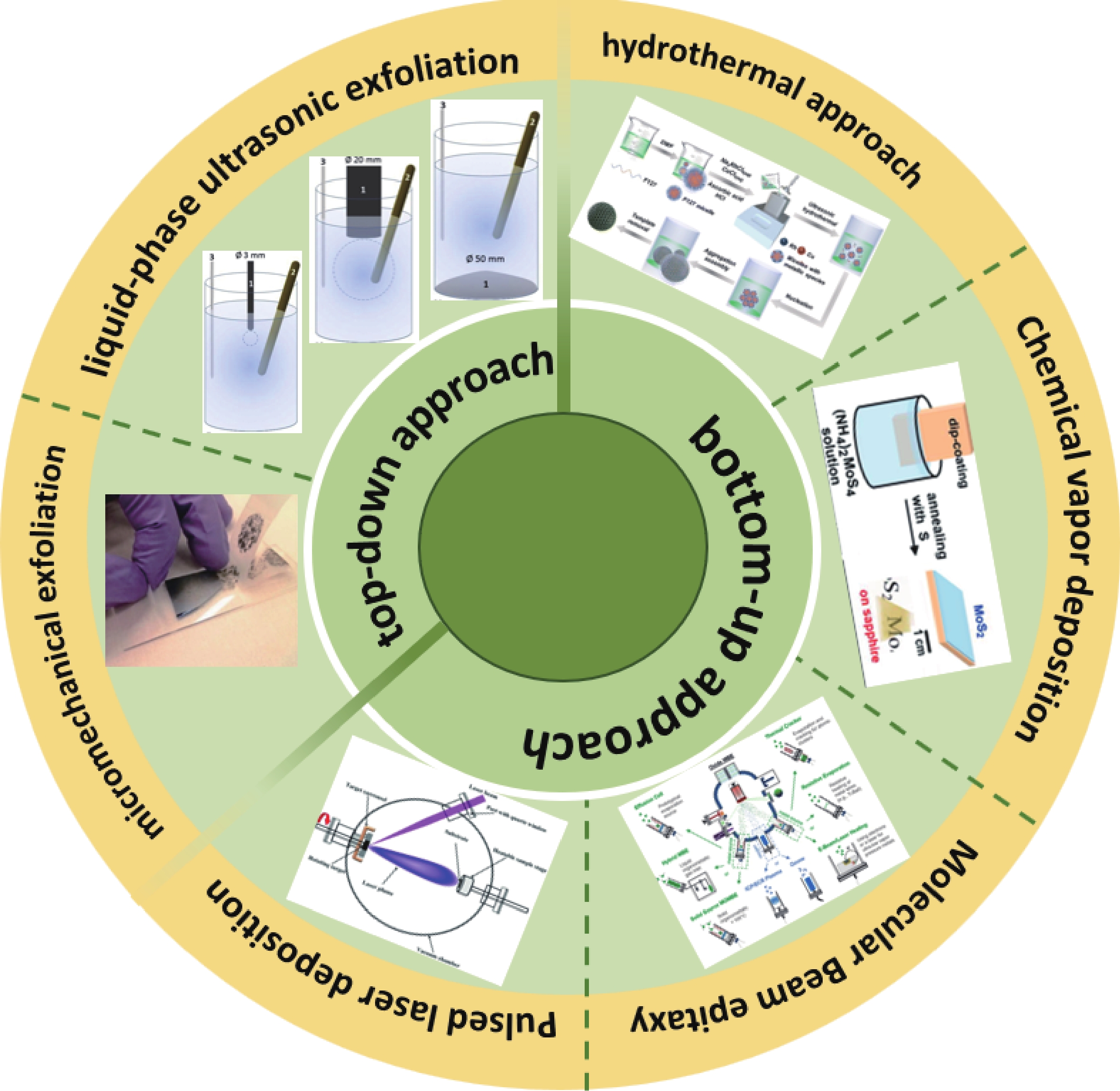
Fig. 1.  (Color online) The growth methods of topological materials encompass a variety of techniques, including mechanical exfoliation, liquid-phase ultrasonic exfoliation, hydrothermal approach, chemical vapor deposition (CVD), molecular beam epitaxy (MBE), and pulsed laser deposition (PLD)[2126].

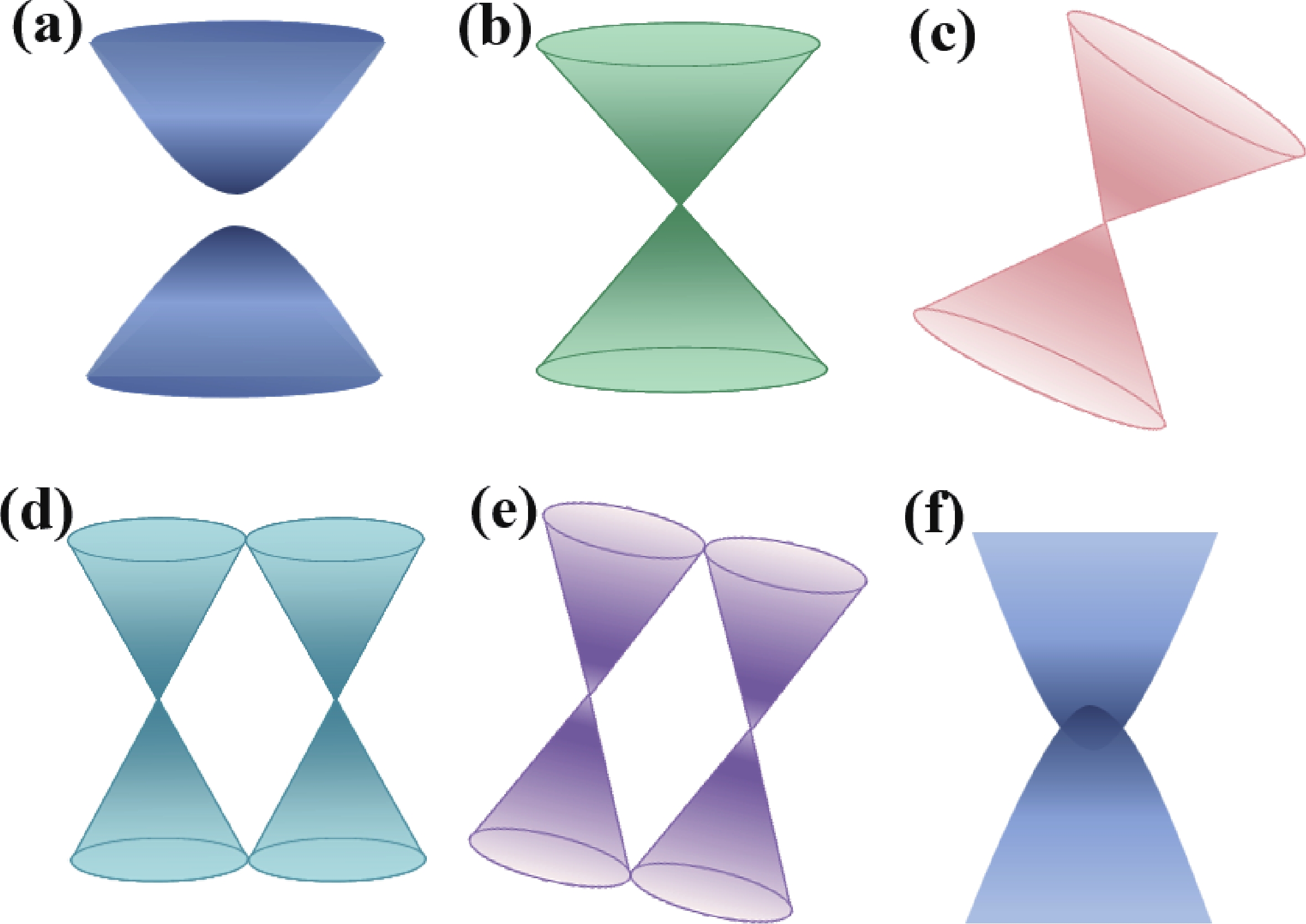
Fig. 2.  (Color online) Topological material band structure diagram. (a) Topological insulator. (b) Type-Ⅰ Dirac semimetal. (c) Type-Ⅱ Dirac semimetal. (d) Type-Ⅰ Weyl semimetal. (e) type-Ⅱ Weyl semimetal. (f) Nodal line semimetal material.

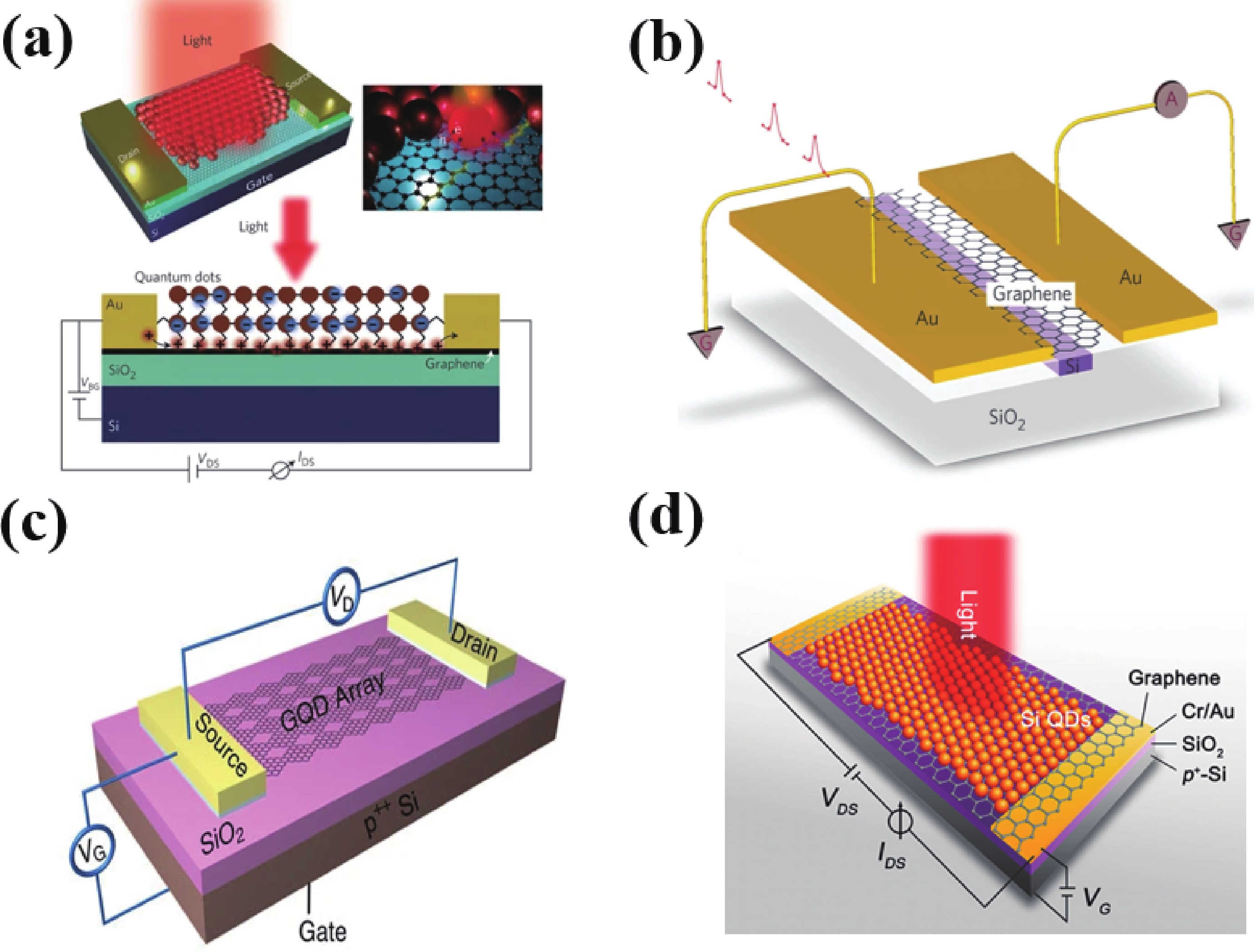
Fig. 3.  (Color online) (a) Schematic of the graphene-quantum dot hybrid phototransistor, in which a graphene flake is deposited onto a Si/SiO2 structure and coated with PbS quantum dots[59]. (b) Schematic of the waveguide-integrated graphene photodetector[60]. (c) The device schematic of a pure single-layer graphene photodetector[61]. (d) Schematic diagram of the structure of the hybrid phototransistor based on B-doped Si QDs and graphene[62].

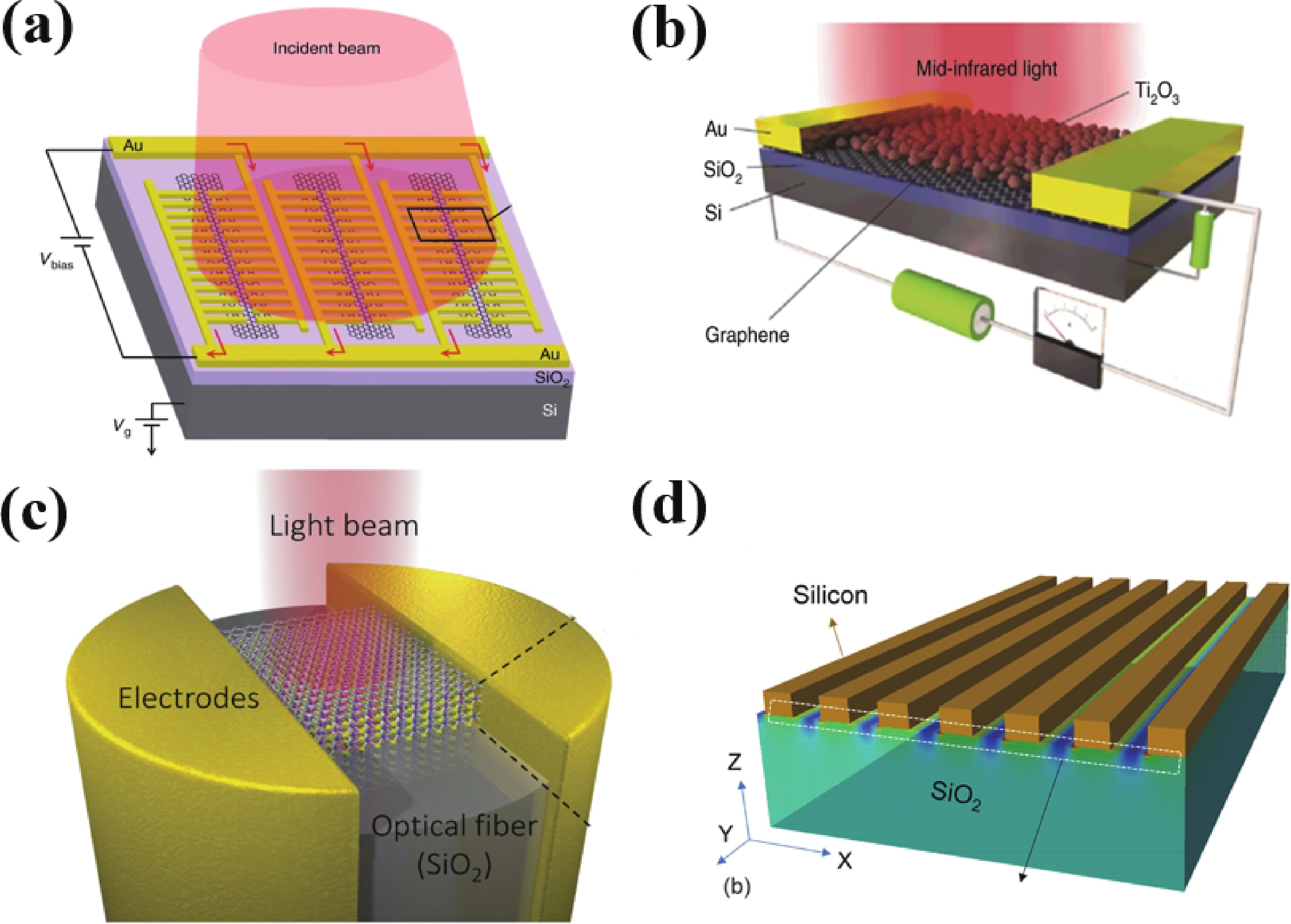
Fig. 4.  (Color online) (a) Schematic of a photodetector based on gold-patched graphene nano-stripes[63]. (b) A schematic diagram of hybrid graphene/Ti2O3 nanoparticle photodetector[64]. (c) 3D schematic view of the FPD illuminated[65]. (d) 3D plot of the silicon grating structure and the simulated field distribution[66].

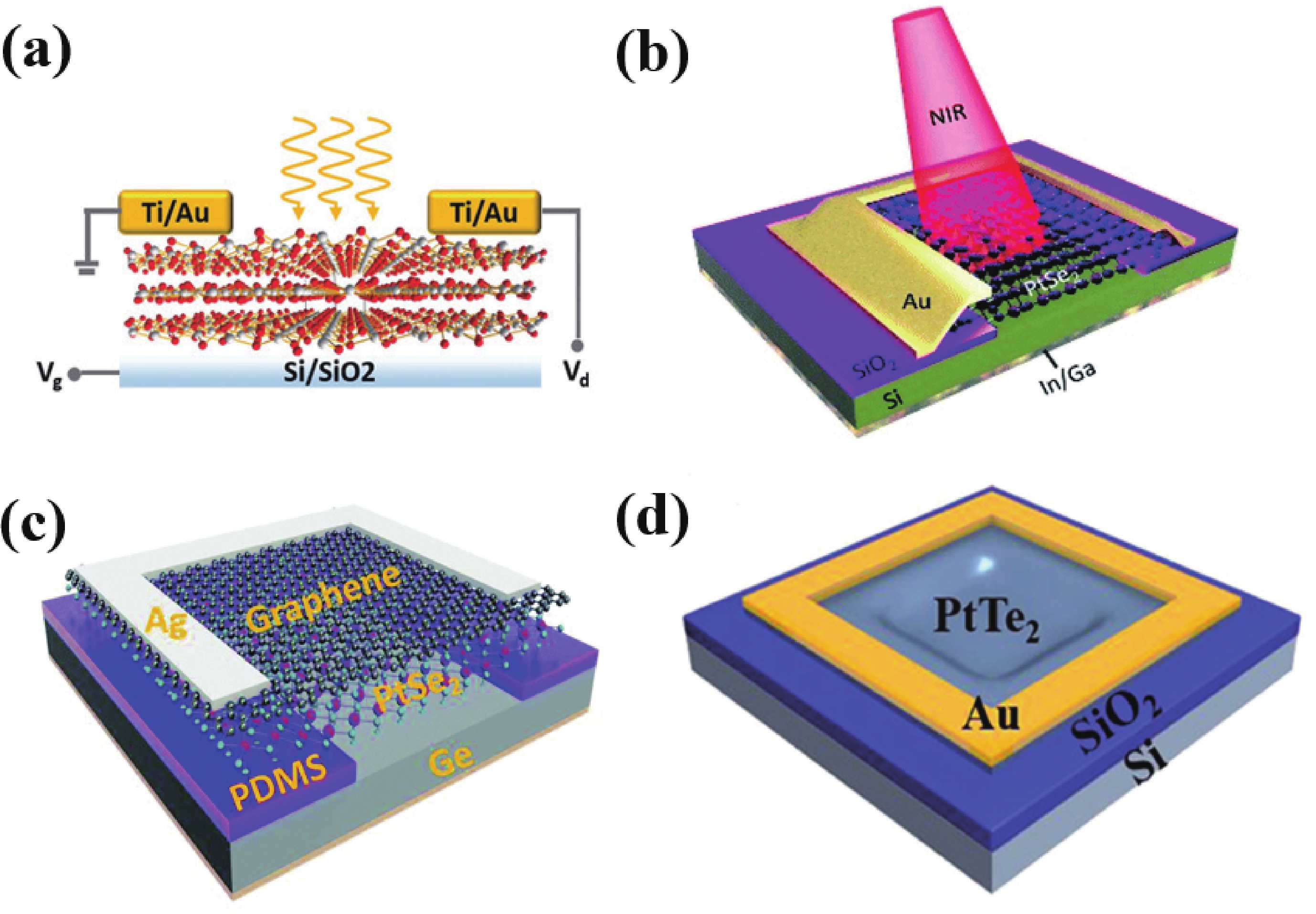
Fig. 5.  (Color online) (a) Schematic diagram of the PdSe2-based photodetector[67]. (b) Schematic of the PtSe2/Si heterojunction photodetector[70]. (c) Schematic of the PtSe2/Ge heterojunction NIR photodetector[71]. (d) Schematic of the PtTe2/Si-based NIRPD[72].

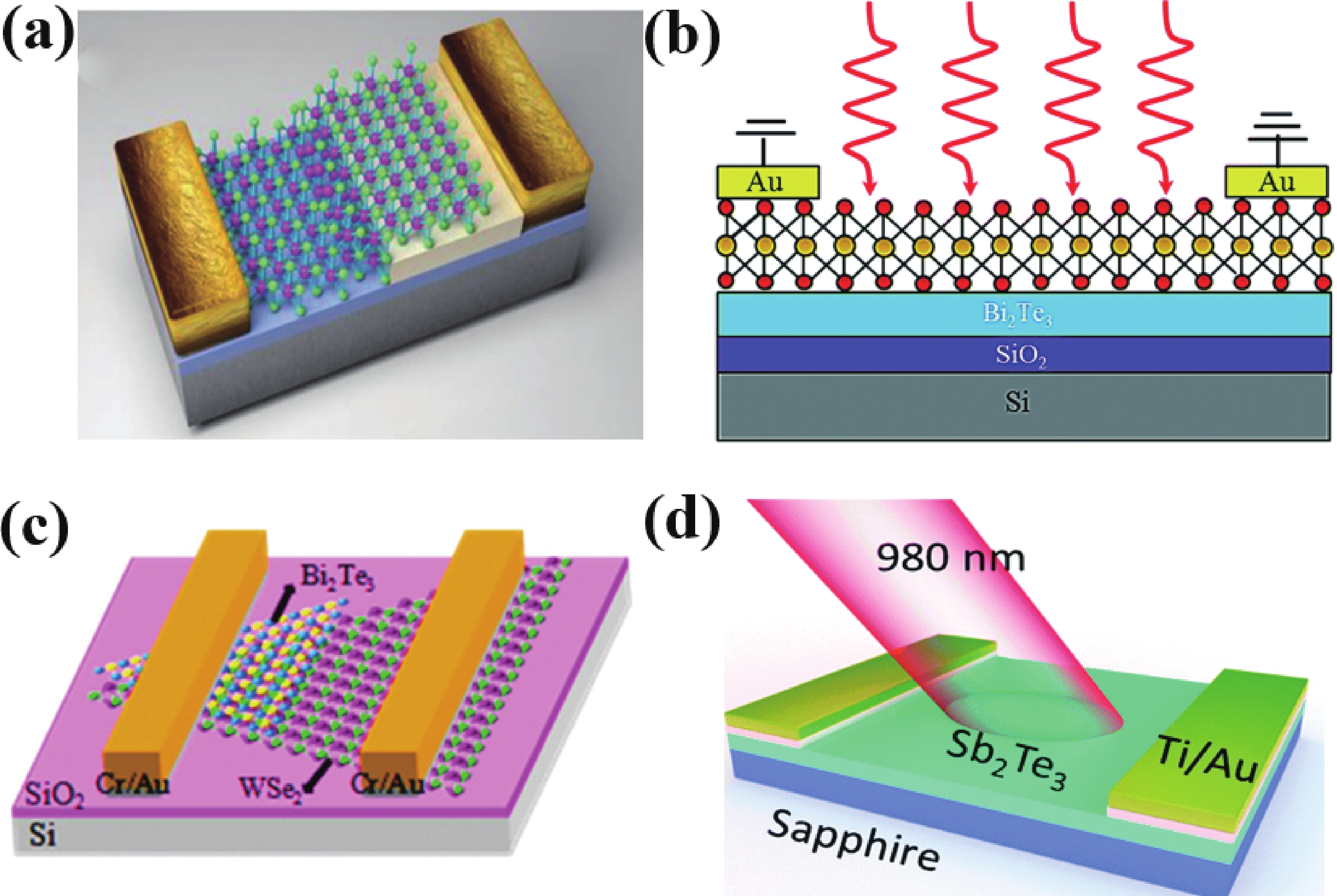
Fig. 6.  (Color online) (a) Schematic diagram of Bi2Se3/MoO3 thin film heterojunction device[76]. (b) The cross-sectional view of the WS2/Bi2Te3 photodetector[78]. (c) Device schematic diagram of the vertically stacked WSe2/Bi2Te3 p−n heterojunction[79]. (d) The schematic illustration of the NIR photodetector based on the topological insulator Sb2Te3 film[80].

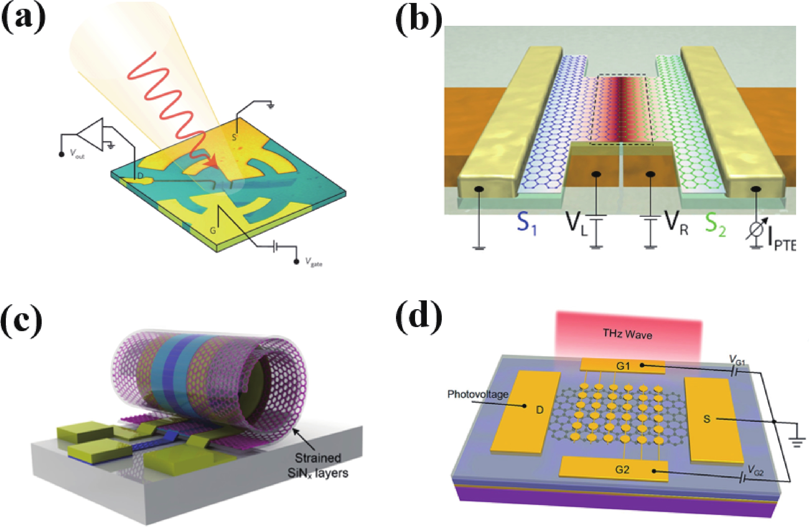
Fig. 7.  (Color online) (a) Schematics of the THz detection configuration in a field-effect transistor (FET) embedding the optical image of the central area of a bilayer graphene-based FET[87]. (b) Schematic diagram of a terahertz detector based on graphene p−n junction integrated with dual-gate dipole antenna[97]. (c) Structure images of the rolled-up 3D GFETs[98]. (d) Schematic of the bent detector[99].

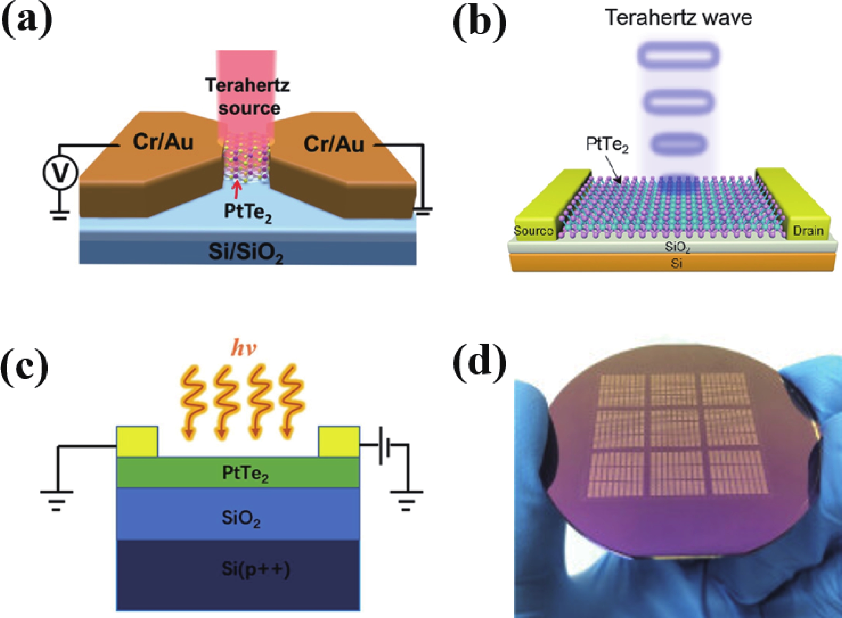
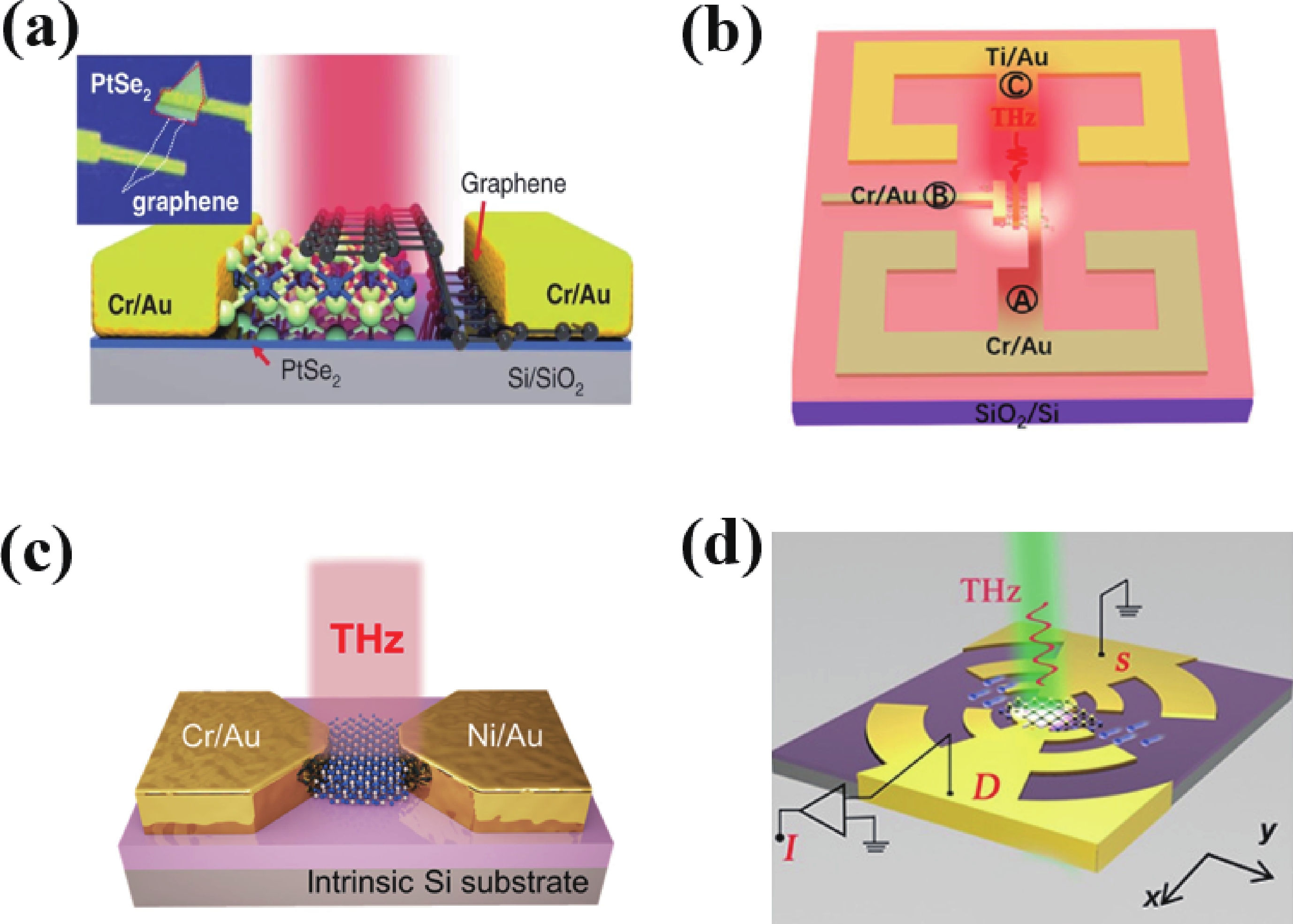
Fig. 8.  (Color online) (a) Schematic representation of the electrical configuration for the bow-tie-type PtTe2-based THz detector[101]. (b) Schematic diagram for the THz photoelectric measurement of the PtTe2 device[102]. (c) PtTe2 photodetector device structure and principle of operation[103]. (d) PtTe2 PD arrays based on the as-grown 2D PtTe2 patterns[104].

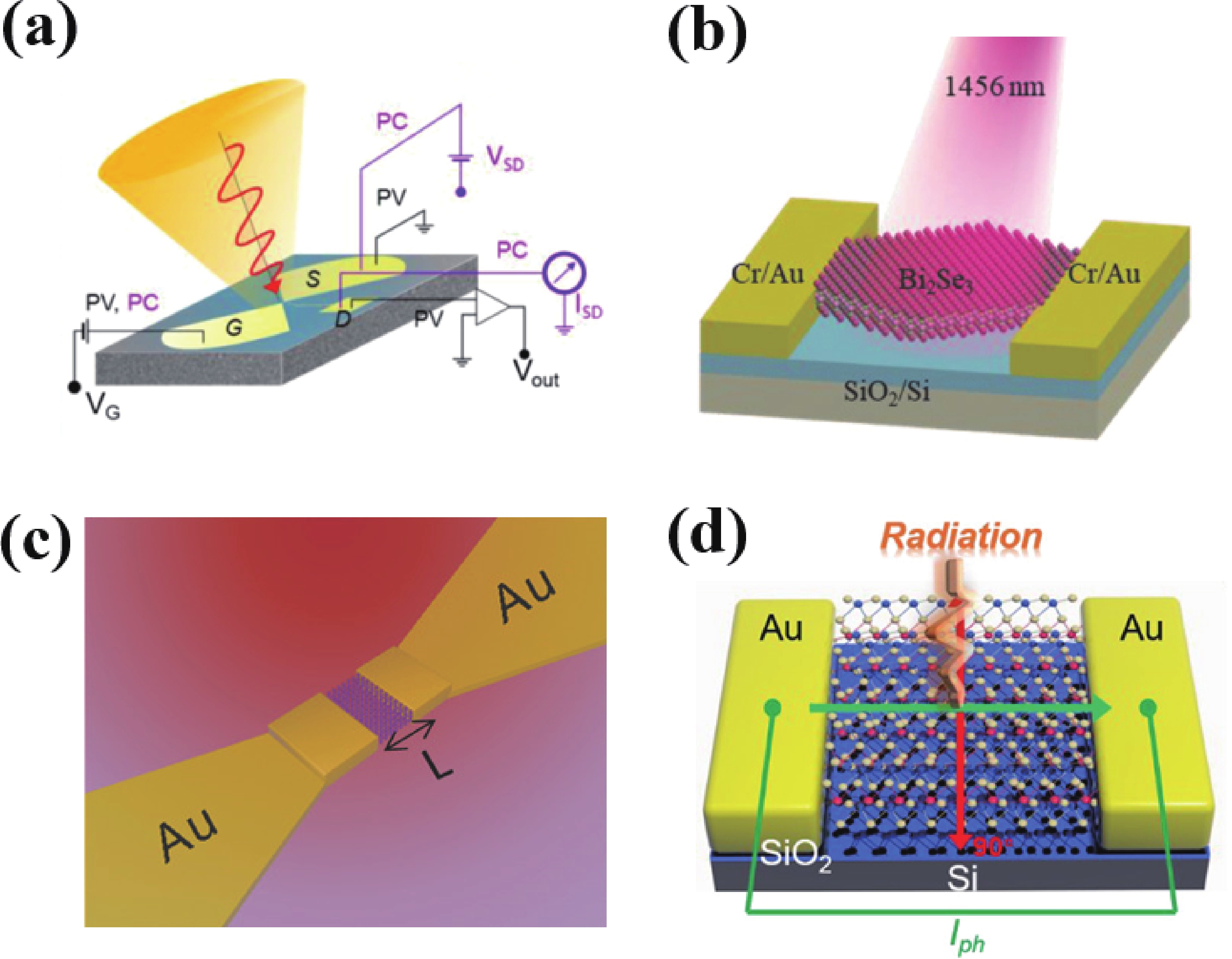
Fig. 9.  (Color online) (a) Schematic diagram of the PtSe2/graphene low-energy photon detector architecture[106]. (b) Schematic diagram of a terahertz photodetector based on an asymmetric cloverleaf antenna structure with PtSe2[107]. (c) Schematic of the PdSe2 PD under THz illumination[108]. (d) Schematic diagram of the PdTe2-based photodetector[109].

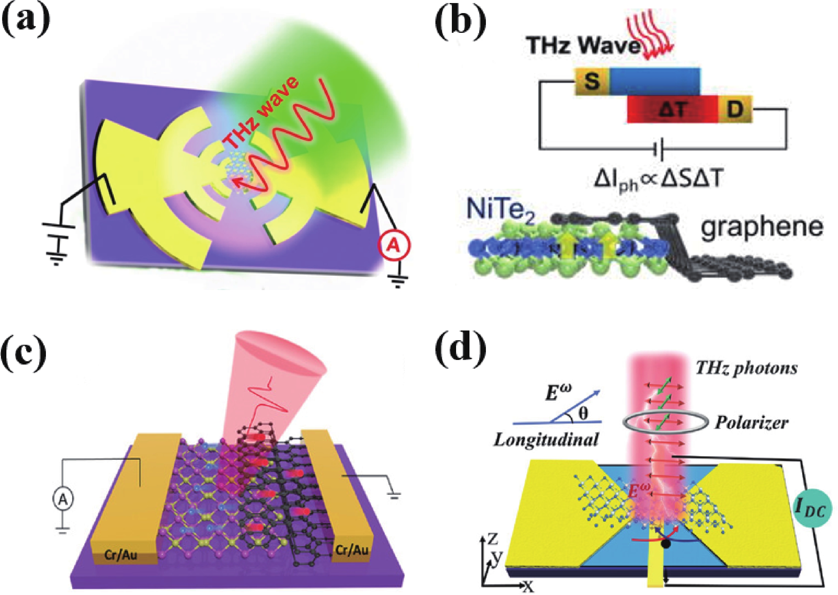
Fig. 10.  (Color online) (a) The experimental setup diagram of a homojunction rectifier based on low-energy Dirac fermions in NiTe2[111]. (b) Schematic of the photothermoelectric mode for detection of the THz wave[112]. (c) Schematic representation of the graphene−NiTeSe−Au photodetector[113]. (d) Schematic of the device architecture made from antenna-coupled Dirac semimetal CoTe2[114].

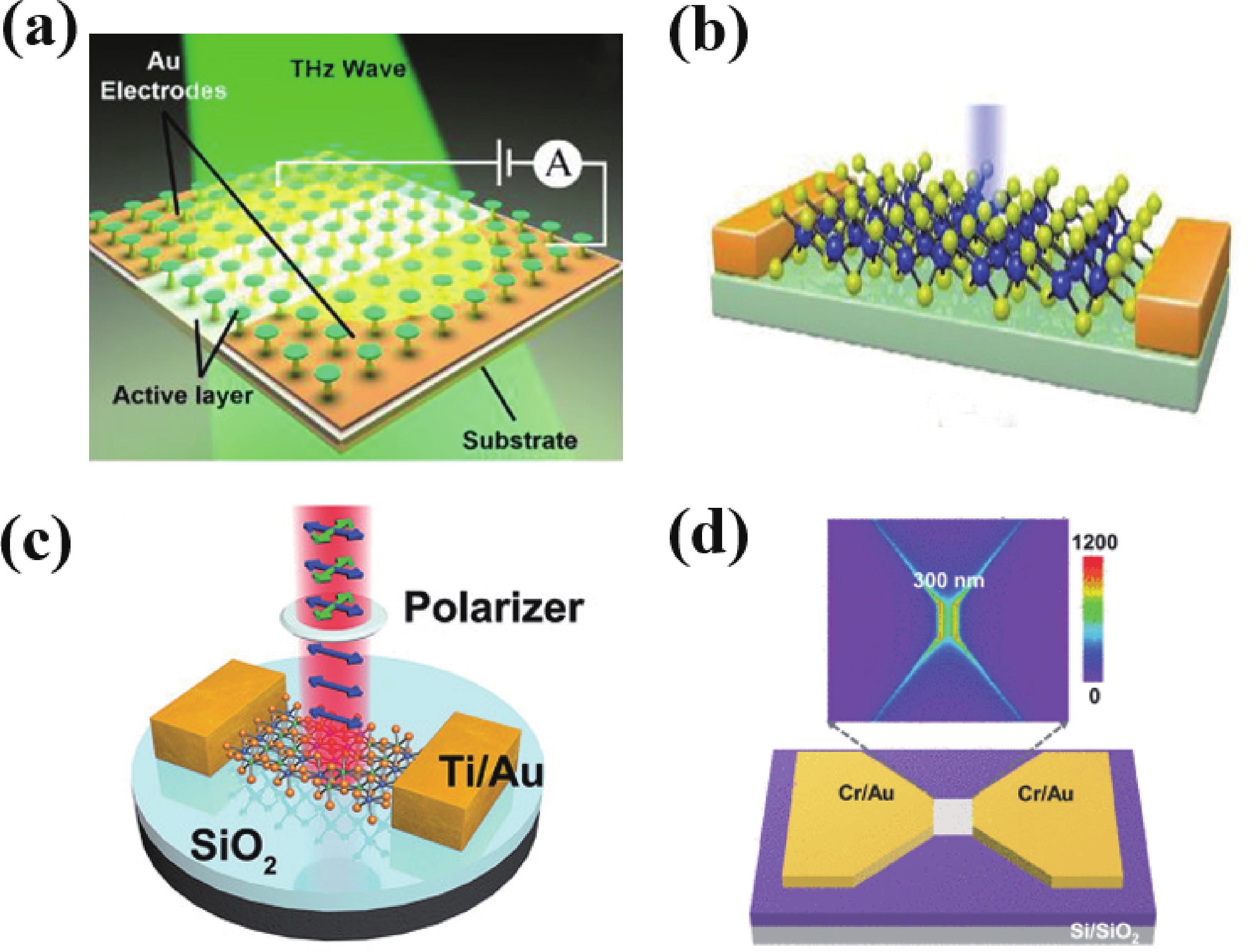
Fig. 11.  (Color online) (a) Schematic diagram of microdisks array covered with WTe2[115]. (b) The photoresponse velocity of the Td-MoTe2 photodetector when subjected to 2.52 THz illumination[118]. (c) Schematic diagram of the experimental setup used to determine the photoresponse based on the NbIrTe4 flakes[119]. (d) Diagram of the NbIrTe4 PD and the E-field distribution[120].

Fig. 12.  (Color online) (a) Schematic diagram of the terahertz detection principle for Bi2Te2.2Se0.8 and Bi2Se3 thin-film nano-scale field-effect transistors[122]. (b) Schematic illustration of the two-terminal Bi2Se3 photodetector[123]. (c) Schematic representation of the subwavelength metal–TI–metal (MTM) structure for the detection of long-wavelength photons at millimeter-wave and THz frequencies[124]. (d) Schematic Diagram of aterahertz photodetector based on MnBi2Te4 thin flakes of magnetic topological insulator[130].

Table 1.   Performance parameters of near-infrared to far-infrared optoelectronic detectors based on topological materials.

Topological
Type
MaterialsWavelengthResponsivity (
A/W)
Response
time
Detectivity (Jones)Refs.
Type-Ⅰ
Dirac semimetal
GrapheneVIS−SWIR5 × 10710 ms7 × 1013[44]
Graphene1450−1590 nm0.1[45]
GrapheneVIS−MIR8.61[61]
GrapheneUV−MIR2.2 × 1093.4−9.0 s1013[62]
GrapheneVIS−IR11.5[63]
Graphene/
Ti2O3
MIR3001.2−2.6 ms7 × 108[64]
Graphene
/MoS2/WS2
VIS−IR17.17 ms[65]
GrapheneIR2403.4 × 1012[66]
Type-Ⅱ Dirac semimetalsPdSe2VIS−MIR7081.31 × 109[67]
PtSe2360−2000 nm0.49[68]
PtSe2VIS−MIR5.51.2 ms7 × 108[69]
PtSe2/SiUV−NIR0.5255.3−170.5 µs3.26 × 1013[70]
PtSe2/GeNIR0.6027.4−16.7 ms6.3 × 1011[71]
PtTe2/Si200−1650 nm0.4063.62 × 1012[72]
Weyl semimetalTaAsVIS−LWIR0.00071.67 × 108[73]
Topological insulatorBi2Se3VIS−NIR3000.4 s7.5 × 109[74]
Graphene/
Bi2Se3
NIR−MIR8.184 µs[75]
Bi2Se3/
MoO3
405−1550 nm1.6 × 10463 µs5.79 × 1011[76]
Bi2Te3/WS2370−1550 nm30.720 ms2.3 × 1011[78]
WSe2/
Bi2Te3
375−1550
nm
20.5210 µs[79]
Sb2Te3NIR21.71.22 × 1011[80]
Sb2Te3/Si250−2400 nm270129.8−132.2 ms1.28 × 1013[81]
DownLoad: CSV

Table 2.   Performance parameters of terahertz detectors based on topological materials.

Topological
Type
MaterialsWavelengthResponsivityResponse
time
NEPRefs.
Type-Ⅰ
Dirac semimetal
Graphene0.3 THz0.15 V/W20 ms30 nW/Hz1/2[87]
Graphene487 GHz2 V/W3 nW/Hz1/2[90]
Graphene0.45 THz764 V/W34 pW/Hz1/2[92]
Graphene1.8−4.2 THz30 ns80 pW/Hz1/2[97]
Graphene3.11 THz0.232 A/W265 ns48 pW/Hz1/2[98]
Type-Ⅱ Dirac semimetalsPtTe20.12 THz3.8 A/W20 µs[101]
Graphene/PtTe20.12 THz1.4 kV/W9 µs[101]
PtTe20.04−0.3 THz30−250 mA/W7/8 µs[102]
PtTe20.3 THz19 mA/W1.01 nW/Hz1/2[103]
PtTe20.02−0.3 THz4.7 µs47 pW/Hz1/2[104]
PtSe20.3 THz0.2 A/W1/1.8 µs38 pW/Hz1/2[106]
PtSe20.028 THz3.267 A/W7 µs3.96 pW/Hz1/2[107]
PdSe20.10 THz0.37A/W7.5 µs900 pW/Hz1/2[108]
PdTe20.12 THz10 A/W1 µs2 pW/Hz1/2[109]
NiTe20.3 THz0.25 A/W89.8 pW/Hz1/2[111]
Graphene/NiTe20.28 THz1.31 A/W8.5 µs17.56 pW/Hz1/2[112]
CoTe20.10−0.30 THz0.1 A/W710 ns1 pW/Hz1/2[114]
Weyl semimetalsWTe20.1 THz8.78 A/W0.74 pW/Hz1/2[115]
MoTe22.52 THz0.53 mA/W20 µs2.65 nW/Hz1/2[118]
NbIrTe40.1 THz5.7 × 104 V/W10.8 µs51 pW/Hz1/2[119]
NbIrTe40.026 THz1.63 A/W0.46 µs3.95 pW/Hz1/2[120]
Nodal-line Dirac semimetalZrGeSe0.1 THz0.56 A/W8.3 µs0.15 nW/Hz1/2[121]
Topological insulatorBi2Se30.3 THz475 A/W60 ms0.36 pW/Hz1/2[124]
MnBi2Te40.275 THz0.74 A/W1 µs13 pW/Hz1/2[130]
DownLoad: CSV
[1]
Atabaki A H, Moazeni S, Pavanello F, et al. Integrating photonics with silicon nanoelectronics for the next generation of systems on a chip. Nature, 2018, 556(7701), 349 doi: 10.1038/s41586-018-0028-z
[2]
Liu J S, Jiang J Z, Wang S P, et al. Fast response organic tandem photodetector for visible and near−infrared digital optical communications. Small, 2021, 17(43), e2101316 doi: 10.1002/smll.202101316
[3]
Pospischil A, Humer M, Furchi M M, et al. CMOS−compatible graphene photodetector covering all optical communication bands. Nat Photonics, 2013, 7(11), 892 doi: 10.1038/nphoton.2013.240
[4]
Watson S, Zhang W K, Tavares J, et al. Resonant tunneling diode photodetectors for optical communications. Micro & Optical Tech Lett, 2019, 61(4), 1121 doi: 10.1002/mop.31689
[5]
Wang F K, Zhang Y, Gao Y, et al. 2D metal chalcogenides for iR photodetection. Small, 2019, 15(30), 1901347 doi: 10.1002/smll.201901347
[6]
Bullock J, Amani M, Cho J, et al. Polarization−resolved black phosphorus/molybdenum disulfide mid−wave infrared photodiodes with high detectivity at room temperature. Nat Photonics, 2018, 12(10), 601 doi: 10.1038/s41566-018-0239-8
[7]
Long M S, Wang P, Fang H H, et al. Progress, challenges, and opportunities for 2D material based photodetectors. Adv Funct Mater, 2019, 29(19), 1803807 doi: 10.1002/adfm.201803807
[8]
Yao J D, Yang G W. 2D material broadband photodetectors. Nanoscale, 2020, 12(2), 454 doi: 10.1039/C9NR09070C
[9]
Wang A Q, Ye X G, Yu D P, et al. Topological semimetal nanostructures: from properties to topotronics. ACS Nano, 2020, 14(4), 3755 doi: 10.1021/acsnano.9b07990
[10]
Wang S, Lin B C, Wang A Q, et al. Quantum transport in Dirac and weyl semimetals: A review. Adv Phys X, 2017, 2(3), 518 doi: 10.1080/23746149.2017.1327329
[11]
Gao H, Venderbos J W F, Kim Y, et al. Topological semimetals from first principles. Annu Rev Mater Res, 2019, 49, 153 doi: 10.1146/annurev-matsci-070218-010049
[12]
Kane C L, Mele E J. Z2 topological order and the quantum spin Hall effect. Phys Rev Lett, 2005, 95(14), 146802 doi: 10.1103/PhysRevLett.95.146802
[13]
Kane C L, Mele E J. Quantum spin Hall effect in graphene. Phys Rev Lett, 2005, 95(22), 226801 doi: 10.1103/PhysRevLett.95.226801
[14]
Gui X, Pletikosic I, Cao H B, et al. A new magnetic topological quantum material candidate by design. ACS Cent Sci, 2019, 5(5), 900 doi: 10.1021/acscentsci.9b00202
[15]
Zhang T T, Jiang Y, Song Z D, et al. Catalogue of topological electronic materials. Nature, 2019, 566(7745), 475 doi: 10.1038/s41586-019-0944-6
[16]
Chan C K, Lindner N H, Refael G, et al. Photocurrents in Weyl semimetals. Phys Rev B, 2017, 95(4), 041104 doi: 10.1103/PhysRevB.95.041104
[17]
Das P K, Di Sante D, Cilento F, et al. Electronic properties of candidate type−II Weyl semimetal WTe2. A review perspective. Electron Struct, 2019, 1(1), 014003 doi: 10.1088/2516-1075/ab0835
[18]
Ma J C, Deng K, Zheng L, et al. Experimental progress on layered topological semimetals. 2d Mater, 2019, 6(3), 032001 doi: 10.1088/2053-1583/ab0902
[19]
Schüffelgen P, Schmitt T, Schleenvoigt M, et al. Exploiting topological matter for Majorana physics and devices. Solid State Electron, 2019, 155, 99 doi: 10.1016/j.sse.2019.03.005
[20]
Wang H C, Wang J. Electron transport in Dirac and weyl semimetals. Chin Phys B, 2018, 27(10), 107402 doi: 10.1088/1674-1056/27/10/107402
[21]
Nunn W, Truttmann T K, Jalan B. A review of molecular−beam epitaxy of wide bandgap complex oxide semiconductors. J Mater Res, 2021, 36(23), 4846 doi: 10.1557/s43578-021-00377-1
[22]
Liu K K, Zhang W, Lee Y H, et al. Growth of large−area and highly crystalline MoS2 thin layers on insulating substrates. Nano Lett, 2012, 12(3), 1538 doi: 10.1021/nl2043612
[23]
Ogugua Simon N, Ntwaeaborwa N O, Swart Hendrik C. Latest development on pulsed laser deposited thin films for advanced luminescence applications. Coatings, 2020, 10(11), 1078
[24]
Huang Y, Sutter E, Shi N N, et al. Reliable exfoliation of large−. ACS Nano, 2015, 9(11), 10612 doi: 10.1021/acsnano.5b04258
[25]
Tyurnina A V, Tzanakis I, Morton J, et al. Ultrasonic exfoliation of graphene in water: A key parameter study. Carbon, 2020, 168, 737 doi: 10.1016/j.carbon.2020.06.029
[26]
Fu S Y, Chu K B, Guo M H, et al. Ultrasonic−assisted hydrothermal synthesis of RhCu alloy nanospheres for electrocatalytic urea production. Chem Commun, 2023, 59(29), 4344 doi: 10.1039/D3CC00102D
[27]
Moore J E. The birth of topological insulators. Nature, 2010, 464(7286), 194 doi: 10.1038/nature08916
[28]
Hasan M Z, Kane C L. Colloquium: Topological insulators. Rev Mod Phys, 2010, 82(4), 3045 doi: 10.1103/RevModPhys.82.3045
[29]
Qi X L, Zhang S C. Topological insulators and superconductors. Rev Mod Phys, 2011, 83(4), 1057 doi: 10.1103/RevModPhys.83.1057
[30]
Andrei Bernevig B, Hughes T L, Zhang S C. Quantum spin Hall effect and topological phase transition in HgTe quantum wells. Science, 2006, 314(5806), 1757 doi: 10.1126/science.1133734
[31]
König M, Buhmann H, Molenkamp L W, et al. The quantum spin Hall effect: Theory and experiment. J Phys Soc Jap, 2008, 77
[32]
Liu C X, Hughes T L, Qi X L, et al. Quantum spin Hall effect in inverted type−II semiconductors. Phys Rev Lett, 2008, 100(23), 236601 doi: 10.1103/PhysRevLett.100.236601
[33]
Zhang H J, Liu C X, Qi X L, et al. Topological insulators in Bi2Se3, Bi2Te3 and Sb2Te3 with a single Dirac cone on the surface. Nat Phys, 2009, 5(6), 438 doi: 10.1038/nphys1270
[34]
Bhattacharyya B, Gupta A, Senguttuvan T D, et al. Topological insulator based dual state photo−switch originating through bulk and surface conduction channels. Phys Status Solidi B, 2018, 255(9), 800340 doi: 10.1002/pssb.201800340
[35]
Culcer D, Cem Keser A, Li Y, et al. Transport in two−dimensional topological materials: Recent developments in experiment and theory. 2D Mater, 2020, 7(2), 022007 doi: 10.1088/2053-1583/ab6ff7
[36]
Zhao Z, Zhang H J, Yuan H T, et al. Pressure induced metallization with absence of structural transition in layered molybdenum diselenide. Nat Commun, 2015, 6(1), 7312 doi: 10.1038/ncomms8312
[37]
Zyuzin A A, Zyuzin A Y. Chiral anomaly and second harmonic generation in Weyl semimetals. Phys Rev B, 2017, 95(8), 085127 doi: 10.1103/PhysRevB.95.085127
[38]
Kang K F, Li T X, Sohn E, et al. Nonlinear anomalous Hall effect in few−layer WTe2. Nat Mater, 2019, 18(4), 324 doi: 10.1038/s41563-019-0294-7
[39]
Bradlyn B, Cano J, Wang Z J, et al. Beyond Dirac and Weyl fermions: Unconventional quasiparticles in conventional crystals. Science, 2016, 353(6299), aaf5037 doi: 10.1126/science.aaf5037
[40]
Liu Z K, Zhou B, Zhang Y, et al. Discovery of a three−dimensional topological Dirac semimetal, Na3Bi. Science, 2014, 343(6173), 864 doi: 10.1126/science.1245085
[41]
Yan M, Huang H Q, Zhang K N, et al. Lorentz−violating type−II Dirac fermions in transition metal dichalcogenide PtTe2. Nat Commun, 2017, 8(1), 257 doi: 10.1038/s41467-017-00280-6
[42]
Soluyanov A A, Gresch D, Wang Z, et al. Type−II Weyl semimetals. Nature, 2015, 527(7579), 495 doi: 10.1038/nature15768
[43]
Mukherjee S P, Carbotte J P. Absorption of circular polarized light in tilted type−I and type−II Weyl semimetals. Phys Rev B, 2017, 96(8), 085114 doi: 10.1103/PhysRevB.96.085114
[44]
Lv B Q, Weng H M, Fu B B, et al. Experimental discovery of weyl semimetal TaAs. Phys Rev X, 2015, 5(3), 031013 doi: 10.1103/PhysRevX.5.031013
[45]
Sun Y, Wu S C, Yan B. Topological surface states and Fermi arcs of the noncentrosymmetric Weyl semimetals TaAs, TaP, NbAs, and NbP. Phys Rev B, 2015, 92(11), 115428 doi: 10.1103/PhysRevB.92.115428
[46]
Zhang C, Ni Z L, Zhang J L, et al. Ultrahigh conductivity in Weyl semimetal NbAs nanobelts. Nat Mater, 2019, 18(5), 482 doi: 10.1038/s41563-019-0320-9
[47]
Wu Y, Mou D X, Jo N H, et al. Observation of Fermi arcs in the type−II Weyl semimetal candidate WTe2. Phys Rev B, 2016, 94(12), 121113 doi: 10.1103/PhysRevB.94.121113
[48]
Ma J C, Gu Q Q, Liu Y N, et al. Nonlinear photoresponse of type−II weyl semimetals. Nat Mater, 2019, 18(5), 476 doi: 10.1038/s41563-019-0296-5
[49]
Burkov A A, Hook M D, Balents L. Topological nodal semimetals. Phys Rev B, 2011, 84(23), 235126 doi: 10.1103/PhysRevB.84.235126
[50]
Hu J, Tang Z J, Liu J Y, et al. Evidence of topological nodal−line fermions in ZrSiSe and ZrSiTe. Phys Rev Lett, 2016, 117(1), 016602 doi: 10.1103/PhysRevLett.117.016602
[51]
Takane D, Wang Z W, Souma S, et al. Dirac−node arc in the topological line−node semimetal HfSiS. Phys Rev B, 2016, 94(12), 121108 doi: 10.1103/PhysRevB.94.121108
[52]
Chen H Y, Liu H, Zhang Z M, et al. Nanostructured photodetectors: From ultraviolet to terahertz. Adv Mater, 2016, 28(3), 403 doi: 10.1002/adma.201503534
[53]
Wong M H, Giraldo J P, Kwak S Y, et al. Nitroaromatic detection and infrared communication from wild−type plants using plant nanobionics. Nat Mater, 2017, 16(2), 264 doi: 10.1038/nmat4771
[54]
Miao J S, Song B, Xu Z H, et al. Single pixel black phosphorus photodetector for near−infrared imaging. Small, 2018, 14(2), 1702082 doi: 10.1002/smll.201702082
[55]
Ye L, Li H, Chen Z F, et al. Near−infrared photodetector based on MoS2/Black phosphorus heterojunction. ACS Photonics, 2016, 3(4), 692 doi: 10.1021/acsphotonics.6b00079
[56]
Novoselov K S, Geim A K, Morozov S V, et al. Electric field effect in atomically thin carbon films. Science, 2004, 306(5696), 666 doi: 10.1126/science.1102896
[57]
Chang H X, Wu H K. Graphene−based nanomaterials: Synthesis, properties, and optical and optoelectronic applications. Adv Funct Mater, 2013, 23(16), 1984 doi: 10.1002/adfm.201202460
[58]
Xia F N, Mueller T, Lin Y M, et al. Ultrafast graphene photodetector. Nat Nanotechnol, 2009, 4(12), 839 doi: 10.1038/nnano.2009.292
[59]
Konstantatos G, Badioli M, Gaudreau L, et al. Hybrid graphene–quantum dot phototransistors with ultrahigh gain. Nat Nanotechnol, 2012, 7(6), 363 doi: 10.1038/nnano.2012.60
[60]
Gan X T, Shiue R J, Gao Y D, et al. Chip−integrated ultrafast graphene photodetector with high responsivity. Nat Photonics, 2013, 7(11), 883 doi: 10.1038/nphoton.2013.253
[61]
Zhang B Y, Liu T, Meng B, et al. Broadband high photoresponse from pure monolayer graphene photodetector. Nat Commun, 2013, 4(1), 1811 doi: 10.1038/ncomms2830
[62]
Ni Z Y, Ma L L, Du S C, et al. Plasmonic silicon quantum dots enabled high−sensitivity ultrabroadband photodetection of graphene−based hybrid phototransistors. ACS Nano, 2017, 11(10), 9854 doi: 10.1021/acsnano.7b03569
[63]
Cakmakyapan S, Lu P K, Navabi A, et al. Gold−patched graphene nano−stripes for high−responsivity and ultrafast photodetection from the visible to infrared regime. Light Sci Appl, 2018, 7(1), 20
[64]
Yu X C, Li Y Y, Hu X N, et al. Narrow bandgap oxide nanoparticles coupled with graphene for high performance mid−infrared photodetection. Nat Commun, 2018, 9(1), 4299 doi: 10.1038/s41467-018-06776-z
[65]
Xiong Y F, Chen J H, Lu Y Q, et al. Broadband optical−fiber−compatible photodetector based on a graphene−MoS2−WS2 heterostructure with a synergetic photogenerating mechanism. Adv Elect Materials, 2019, 5(1), 1800562 doi: 10.1002/aelm.201800562
[66]
Jiang H, Wei J X, Sun F Y, et al. Enhanced photogating effect in graphene photodetectors via potential fluctuation engineering. ACS Nano, 2022, 16(3), 4458 doi: 10.1021/acsnano.1c10795
[67]
Liang Q J, Wang Q X, Zhang Q, et al. High−performance, room temperature, ultra−broadband photodetectors based on air−stable PdSe2. Adv Mater, 2019, 31(24), 1807609 doi: 10.1002/adma.201807609
[68]
Yim C, McEvoy N, Riazimehr S, et al. Wide spectral photoresponse of layered platinum diselenide−based photodiodes. Nano Lett, 2018, 18(3), 1794 doi: 10.1021/acs.nanolett.7b05000
[69]
Yu X, Yu P, Wu D, et al. Atomically thin noble metal dichalcogenide: A broadband mid−infrared semiconductor. Nat Commun, 2018, 9(1), 1545 doi: 10.1038/s41467-018-03935-0
[70]
Xie C, Zeng L H, Zhang Z X, et al. High−performance broadband heterojunction photodetectors based on multilayered PtSe2 directly grown on a Si substrate. Nanoscale, 2018, 10(32), 15285 doi: 10.1039/C8NR04004D
[71]
Wang L, Li J J, Fan Q, et al. A high−performance near−infrared light photovoltaic detector based on a multilayered PtSe2/Ge heterojunction. J Mater Chem C, 2019, 7(17), 5019 doi: 10.1039/C9TC00797K
[72]
Tong X W, Lin Y N, Huang R, et al. Direct tellurization of Pt to synthesize 2D PtTe2 for high−performance broadband photodetectors and NIR image sensors. ACS Appl Mater & Interfaces, 2020, 12, 53921
[73]
Chi S M, Li Z L, Xie Y, et al. A wide−range photosensitive weyl semimetal single crystal—TaAs. Adv Mater, 2018, 30(43), 1801372 doi: 10.1002/adma.201801372
[74]
Sharma A, Bhattacharyya B, Srivastava A K, et al. High performance broadband photodetector using fabricated nanowires of bismuth selenide. Sci Rep, 2016, 6(1), 19138 doi: 10.1038/srep19138
[75]
Kim J, Park S, Jang H, et al. Highly sensitive, gate−tunable, room−temperature mid−infrared photodetection based on graphene–Bi2Se3 heterostructure. ACS Photonics, 2017, 4(3), 482 doi: 10.1021/acsphotonics.6b00972
[76]
Yang M, Han Q, Liu X C, et al. Ultrahigh stability 3D TI Bi2Se3/MoO3 thin film heterojunction infrared photodetector at optical communication waveband. Adv Funct Mater, 2020, 30(12), 1909659 doi: 10.1002/adfm.201909659
[77]
Yao J D, Shao J M, Li S W, et al. Polarization dependent photocurrent in the Bi2Te3 topological insulator film for multifunctional photodetection. Sci Rep, 2015, 5(1), 14184 doi: 10.1038/srep14184
[78]
Yao J D, Zheng Z Q, Yang G W. Layered−material WS2/topological insulator Bi2Te3 heterostructure photodetector with ultrahigh responsivity in the range from 370 to 1550 nm. J Mater Chem C, 2016, 4(33), 7831 doi: 10.1039/C6TC01453D
[79]
Liu H W, Zhu X L, Sun X X, et al. Self−powered broad−band photodetectors based on vertically stacked WSe2/Bi2Te3 p–n heterojunctions. ACS Nano, 2019, 13(11), 13573 doi: 10.1021/acsnano.9b07563
[80]
Zheng K, Luo L B, Zhang T F, et al. Optoelectronic characteristics of a near infrared light photodetector based on a topological insulator Sb2Te3 film. J Mater Chem C, 2015, 3(35), 9154 doi: 10.1039/C5TC01772F
[81]
Zhang Y P, Tang L B, Teng K S. High performance broadband photodetectors based on Sb2Te3/n−Si heterostructure. Nanotechnology, 2020, 31(30), 304002 doi: 10.1088/1361-6528/ab851c
[82]
Ferguson B, Zhang X C. Materials for terahertz science and technology. Nat Mater, 2002, 1(1), 26 doi: 10.1038/nmat708
[83]
Wang Y X, Wu W D, Zhao Z R. Recent progress and remaining challenges of 2D material−based terahertz detectors. Infrared Phys Technol, 2019, 102, 103024
[84]
Guo X G, Cao J C, Zhang R, et al. Recent progress in terahertz quantum−well photodetectors, selected topics in quantum electronics. IEEE J Sel Top Quantum Electron , 2013, 19, 8500508
[85]
Qiu Q X, Huang Z M. Photodetectors of 2D materials from ultraviolet to terahertz waves. Adv Mater, 2021, 33(15), 2008126 doi: 10.1002/adma.202008126
[86]
Kawano Y. Wide−band frequency−tunable terahertz and infrared detection with graphene. Nanotechnology, 2013, 24(21), 214004 doi: 10.1088/0957-4484/24/21/214004
[87]
Vicarelli L, Vitiello M S, Coquillat D, et al. Graphene field−effect transistors as room−temperature terahertz detectors. Nat Mater, 2012, 11(10), 865 doi: 10.1038/nmat3417
[88]
Cai X H, Sushkov A B, Suess R J, et al. Sensitive room−temperature terahertz detection via the photothermoelectric effect in graphene. Nat Nanotechnol, 2014, 9(10), 814 doi: 10.1038/nnano.2014.182
[89]
Cai X, Sushkov A B, Jadidi M M, et al. Plasmon−enhanced terahertz photodetection in graphene. Nano Lett, 2015, 15(7), 4295 doi: 10.1021/acs.nanolett.5b00137
[90]
Yang X X, Vorobiev A, Generalov A, et al. A flexible graphene terahertz detector. Appl Phys Lett, 2017, 111(2), 021102 doi: 10.1063/1.4993434
[91]
Zak A, Andersson M A, Bauer M, et al. Antenna−integrated 0.6 THz FET direct detectors based on CVD graphene. Nano Lett, 2014, 14(10), 5834 doi: 10.1021/nl5027309
[92]
Auton G, But D B, Zhang J, et al. Terahertz detection and imaging using graphene ballistic rectifiers. Nano Lett, 2017, 17(11), 7015 doi: 10.1021/acs.nanolett.7b03625
[93]
Song A M, Lorke A, Kriele A, et al. Nonlinear electron transport in an asymmetric microjunction: A ballistic rectifier. Phys Rev Lett, 1998, 80(17), 3831 doi: 10.1103/PhysRevLett.80.3831
[94]
Woessner A, Lundeberg M B, Gao Y D, et al. Highly confined low−loss plasmons in graphene−boron nitride heterostructures. Nat Mater, 2015, 14(4), 421 doi: 10.1038/nmat4169
[95]
Ni G X, McLeod A S, Sun Z, et al. Fundamental limits to graphene plasmonics. Nature, 2018, 557(7706), 530 doi: 10.1038/s41586-018-0136-9
[96]
Bandurin D A, Svintsov D, Gayduchenko I, et al. Resonant terahertz detection using graphene plasmons. Nat Commun, 2018, 9(1), 5392 doi: 10.1038/s41467-018-07848-w
[97]
Castilla S, Terrés B, Autore M, et al. Fast and sensitive terahertz detection using an antenna−integrated graphene pn junction. Nano Lett, 2019, 19(5), 2765 doi: 10.1021/acs.nanolett.8b04171
[98]
Deng T, Zhang Z H, Liu Y X, et al. Three−dimensional graphene field−effect transistors as high−performance photodetectors. Nano Lett, 2019, 19(3), 1494 doi: 10.1021/acs.nanolett.8b04099
[99]
Chen M, Wang Y X, Zhao Z R. Monolithic metamaterial−integrated graphene terahertz photodetector with wavelength and polarization selectivity. ACS Nano, 2022, 16(10), 17263 doi: 10.1021/acsnano.2c07968
[100]
Sadhukhan K, Politano A, Agarwal A. Novel undamped gapless plasmon mode in a tilted type−II Dirac semimetal. Phys Rev Lett, 2020, 124(4), 046803 doi: 10.1103/PhysRevLett.124.046803
[101]
Xu H, Guo C, Zhang J Z, et al. PtTe2−based type−II Dirac semimetal and its van der waals heterostructure for sensitive room temperature terahertz photodetection. Small, 2019, 15(52), 1903362 doi: 10.1002/smll.201903362
[102]
Yang Y, Zhang K X, Zhang L B, et al. Controllable growth of type−II Dirac semimetal PtTe2 atomic layer on Au substrate for sensitive room temperature terahertz photodetection. InfoMat, 2021, 3(6), 705 doi: 10.1002/inf2.12193
[103]
Zhang K X, Xing H Z, Wang L. PtTe2−based terahertz photodetector integrated with an interdigital antenna. Infrared Phys Technol, 2022, 123, 104168
[104]
Dong Z, Yu W Z, Zhang L B, et al. Wafer−scale patterned growth of type−II Dirac semimetal platinum ditelluride for sensitive room−temperature terahertz photodetection. InfoMat, 2023, 5(5), e12403 doi: 10.1002/inf2.12403
[105]
Li Y W, Xia Y, Ekahana S A, et al. Topological origin of the type−II Dirac fermions in PtSe2. Phys Rev Materials, 2017, 1(7), 074202 doi: 10.1103/PhysRevMaterials.1.074202
[106]
Wang L, Han L, Guo W L, et al. Hybrid Dirac semimetal−based photodetector with efficient low−energy photon harvesting. Light Sci Appl, 2022, 11(1), 53 doi: 10.1038/s41377-022-00741-8
[107]
Lv X Y, Zhang K X, Jiang M J, et al. Enhancement of terahertz response in a microstructure−integrated−type−II Dirac semimetal. AIP Adv, 2023, 13(11), 115223 doi: 10.1063/5.0175151
[108]
Dong Z, Yu W, Zhang L B, et al. Highly efficient, ultrabroad PdSe2 phototransistors from visible to terahertz driven by mutiphysical mechanism. ACS Nano, 2021, 15(12), 20403 doi: 10.1021/acsnano.1c08756
[109]
Guo C, Hu Y B, Chen G, et al. Anisotropic ultrasensitive PdTe2−based phototransistor for room−temperature long−wavelength detection. Sci Adv, 2020, 6(36), eabb6500 doi: 10.1126/sciadv.abb6500
[110]
Xu C Q, Li B, Jiao W H, et al. Topological type−II Dirac fermions approaching the fermi level in a transition metal dichalcogenide NiTe2. Chem Mater, 2018, 30(14), 4823 doi: 10.1021/acs.chemmater.8b02132
[111]
Zhang L B, Chen Z, Zhang K X, et al. High−frequency rectifiers based on type−II Dirac fermions. Nat Commun, 2021, 12(1), 1584 doi: 10.1038/s41467-021-21906-w
[112]
Shen J Z, Xing H Z, Wang L, et al. A van der Waals heterostructure based on nickel telluride and graphene with spontaneous high−frequency photoresponse. Appl Phys Lett, 2022, 120(6), 063501 doi: 10.1063/5.0082574
[113]
Zhang K X, Hu Z, Zhang L B, et al. Ultrasensitive self−driven terahertz photodetectors based on low−energy type−II Dirac fermions and related van der Waals heterojunctions. Small, 2023, 19(1), 2205329 doi: 10.1002/smll.202205329
[114]
Hu Z, Zhang L B, Chakraborty A, et al. Terahertz nonlinear Hall rectifiers based on spin−polarized topological electronic states in 1T−CoTe2. Adv Mater, 2023, 35(10), 2209557 doi: 10.1002/adma.202209557
[115]
Song Q, Zhou Z W, Zhu G, et al. Microdisk array based Weyl semimetal nanofilm terahertz detector. Nanophotonics, 2022, 11(16), 3595 doi: 10.1515/nanoph-2022-0227
[116]
Sun Y, Wu S C, Ali M N, et al. Prediction of Weyl semimetal in orthorhombic MoTe2. Phys Rev B, 2015, 92(16), 161107 doi: 10.1103/PhysRevB.92.161107
[117]
Jiang J, Liu Z K, Sun Y, et al. Signature of type−II weyl semimetal phase in MoTe2. Nat Commun, 2017, 8(1), 13973 doi: 10.1038/ncomms13973
[118]
Yang Q, Wang X M, He Z H, et al. A centimeter−scale type−II Weyl semimetal for flexible and fast ultra−broadband photodetection from ultraviolet to sub−millimeter wave regime. Adv Sci, 2023, 10(17), 2205609 doi: 10.1002/advs.202205609
[119]
Zhang J T, Zhang T N, Yan L, et al. Colossal room−temperature terahertz topological response in type−II Weyl semimetal NbIrTe4. Adv Mater, 2022, 34(42), 2204621 doi: 10.1002/adma.202204621
[120]
Yang L, Wang D, Dong Z, et al. Low−power polarization sensitive terahertz photodetection driven by ternary type−II Weyl semimetal NbIrTe4. IEEE Electron Device Lett, 2023, 44(4), 686 doi: 10.1109/LED.2023.3250468
[121]
Zhang L B, Dong Z, Wang L, et al. Ultrasensitive and self‐powered terahertz detection driven by nodal-line Dirac fermions and van der Waals architecture. Adv Sci, 2021, 8(23), 2102088 doi: 10.1002/advs.202102088
[122]
Viti L, Coquillat D, Politano A, et al. Plasma−wave terahertz detection mediated by topological insulators surface states. Nano Lett, 2016, 16(1), 80 doi: 10.1021/acs.nanolett.5b02901
[123]
Wang F K, Li L G, Huang W J, et al. Submillimeter 2D Bi2Se3 flakes toward high−performance infrared photodetection at optical communication wavelength. Adv Funct Materials, 2018, 28(33), 1802707 doi: 10.1002/adfm.201802707
[124]
Tang W W, Politano A, Guo C, et al. Ultrasensitive room−temperature terahertz direct detection based on a bismuth selenide topological insulator. Adv Funct Mater, 2018, 28(31), 1801786 doi: 10.1002/adfm.201801786
[125]
Yu R, Zhang W, Zhang H J, et al. Quantized anomalous Hall . Science, 2010, 329(5987), 61 doi: 10.1126/science.1187485
[126]
Chang C Z, Zhao W W, Kim D Y, et al. High−precision realization of robust quantum anomalous Hall state in a hard ferromagnetic topological insulator. Nat Mater, 2015, 14(5), 473
[127]
Heremans J P, Cava R J, Samarth N. Tetradymites as thermoelectrics and topological insulators. Nat Rev Mater, 2017, 2(10), 17049 doi: 10.1038/natrevmats.2017.49
[128]
Wang H, Qian X F. Electrically and magnetically switchable nonlinear photocurrent in РТ−symmetric magnetic topological quantum materials. NPJ Comput Mater, 2020, 6(1), 199 doi: 10.1038/s41524-020-00462-9
[129]
Zhang Y, Fu L. Terahertz detection based on nonlinear Hall effect without magnetic field. Proc Natl Acad Sci USA, 2021, 118(21), e2100736118 doi: 10.1073/pnas.2100736118
[130]
Guo C, Chen Z, Yu X B, et al. Ultrasensitive anisotropic room−temperature terahertz photodetector based on an intrinsic magnetic topological insulator MnBi2Te4. Nano Lett, 2022, 22(18), 7492 doi: 10.1021/acs.nanolett.2c02434
  • Search

    Advanced Search >>

    GET CITATION

    shu

    Export: BibTex EndNote

    Article Metrics

    Article views: 233 Times PDF downloads: 45 Times Cited by: 0 Times

    History

    Received: 29 January 2025 Revised: 25 February 2025 Online: Uncorrected proof: 18 March 2025

    Catalog

      Email This Article

      User name:
      Email:*请输入正确邮箱
      Code:*验证码错误
      Zhaowen Bao, Yiming Wang, Kaixuan Zhang, Yingdong Wei, Xiaokai Pan, Zhen Hu, Shiqi Lan, Yichong Zhang, Xiaoyun Wang, Huichuan Fan, Hongfei Wu, Lei Yang, Zhiyuan Zhou, Xin Sun, Yulu Chen, Lin Wang. Topological materials-based photodetectors from the infrared to terahertz range[J]. Journal of Semiconductors, 2025, In Press. doi: 10.1088/1674-4926/25010010 ****Z W Bao, Y M Wang, K X Zhang, Y D Wei, X K Pan, Z Hu, S Q Lan, Y C Zhang, X Y Wang, H C Fan, H F Wu, L Yang, Z Y Zhou, X Sun, Y L Chen, and L Wang, Topological materials-based photodetectors from the infrared to terahertz range[J]. J. Semicond., 2025, 46(8), 081401 doi: 10.1088/1674-4926/25010010
      Citation:
      Zhaowen Bao, Yiming Wang, Kaixuan Zhang, Yingdong Wei, Xiaokai Pan, Zhen Hu, Shiqi Lan, Yichong Zhang, Xiaoyun Wang, Huichuan Fan, Hongfei Wu, Lei Yang, Zhiyuan Zhou, Xin Sun, Yulu Chen, Lin Wang. Topological materials-based photodetectors from the infrared to terahertz range[J]. Journal of Semiconductors, 2025, In Press. doi: 10.1088/1674-4926/25010010 ****
      Z W Bao, Y M Wang, K X Zhang, Y D Wei, X K Pan, Z Hu, S Q Lan, Y C Zhang, X Y Wang, H C Fan, H F Wu, L Yang, Z Y Zhou, X Sun, Y L Chen, and L Wang, Topological materials-based photodetectors from the infrared to terahertz range[J]. J. Semicond., 2025, 46(8), 081401 doi: 10.1088/1674-4926/25010010

      Topological materials-based photodetectors from the infrared to terahertz range

      DOI: 10.1088/1674-4926/25010010
      CSTR: 32376.14.1674-4926.25010010
      More Information
      • Zhaowen Bao got her BS degree from Shandong Normal University in 2023. At present, she is pursuing a Master’s degree at ShanghaiTech University and is engaged in research under the supervision of Dr. Chen Xiaoshuang and Dr. Wang Lin at the Shanghai Institute of Technical Physics. Her research is concentrated on terahertz photodetection
      • Lin Wang currently serves as a researcher at the Shanghai Institute of Technical Physics. He obtained his Ph.D. from the Shanghai Institute of Technical Physics, Chinese Academy of Sciences. His primary research interests revolve around national significant demands such as deep space exploration, atmospheric remote sensing, and 6G communication. He focuses on the development of new quantum-enhanced detection mechanisms and application verification for infrared and terahertz low-energy excitation, as well as the advancement of new materials, principles, and devices based on the quantum state control of low-dimensional structures
      • Corresponding author: vincent.wang0020@outlook.comwanglin@mail.sitp.ac.cn
      • Received Date: 2025-01-29
      • Revised Date: 2025-02-25
      • Available Online: 2025-03-18

      Catalog

        /

        DownLoad:  Full-Size Img  PowerPoint
        Return
        Return