


Fig. 1.
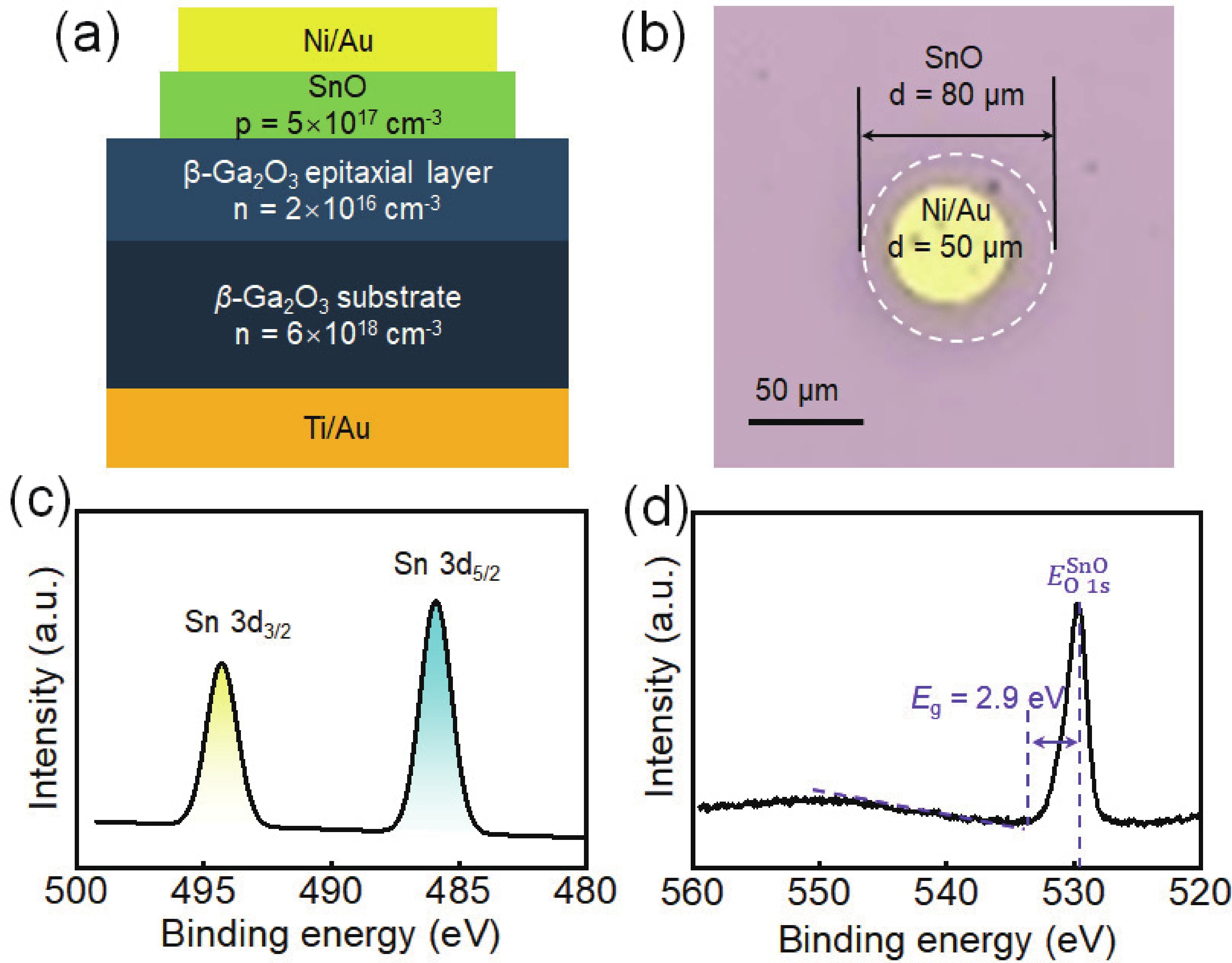
(Color online) (a) Cross-sectional schematic and (b) top-view optical microphotograph of vertical SnO/β-Ga2O3 HJD. (c) Sn 3d core level spectrum and (d) O 1s core level spectra of the SnO film.
ARTICLES
Xia Wu1, Chenyang Huang1, Xiuxing Xu1, Jun Wang1, Xinwang Yao1, Yanfang Liu2, Xiujuan Wang1, Chunyan Wu1, and Linbao Luo1
Corresponding author: Chunyan Wu, cywu@hfut.edu.cn
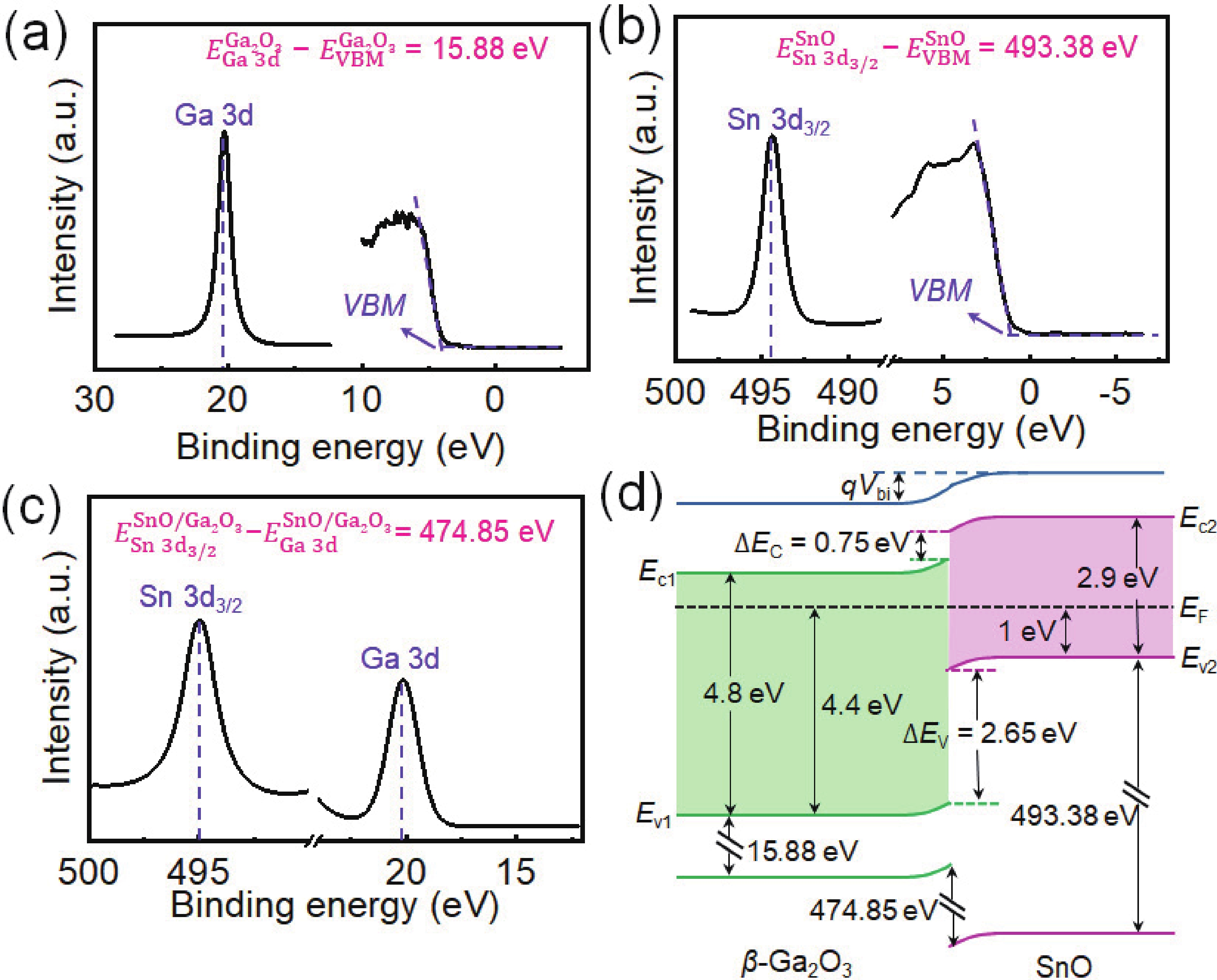
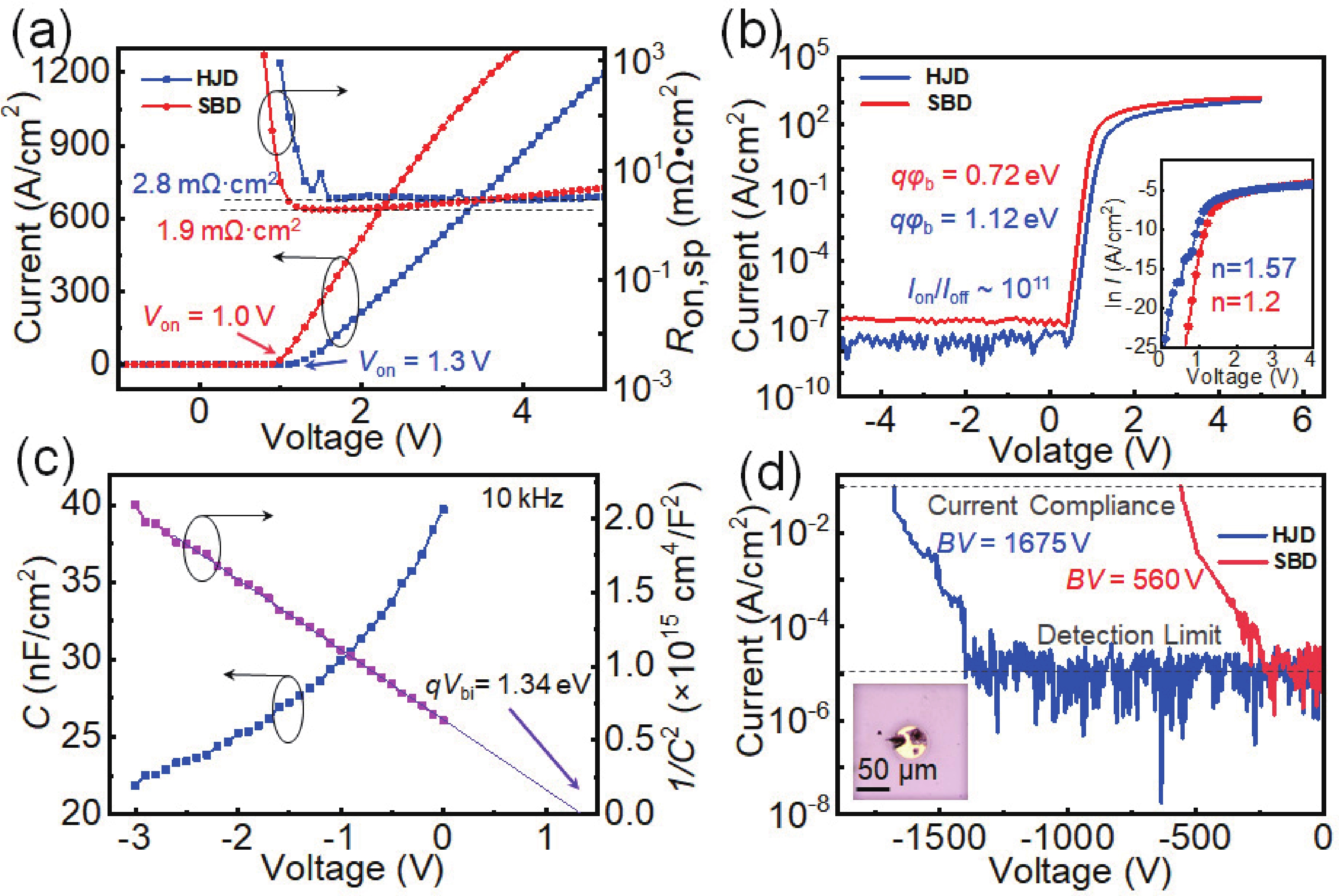
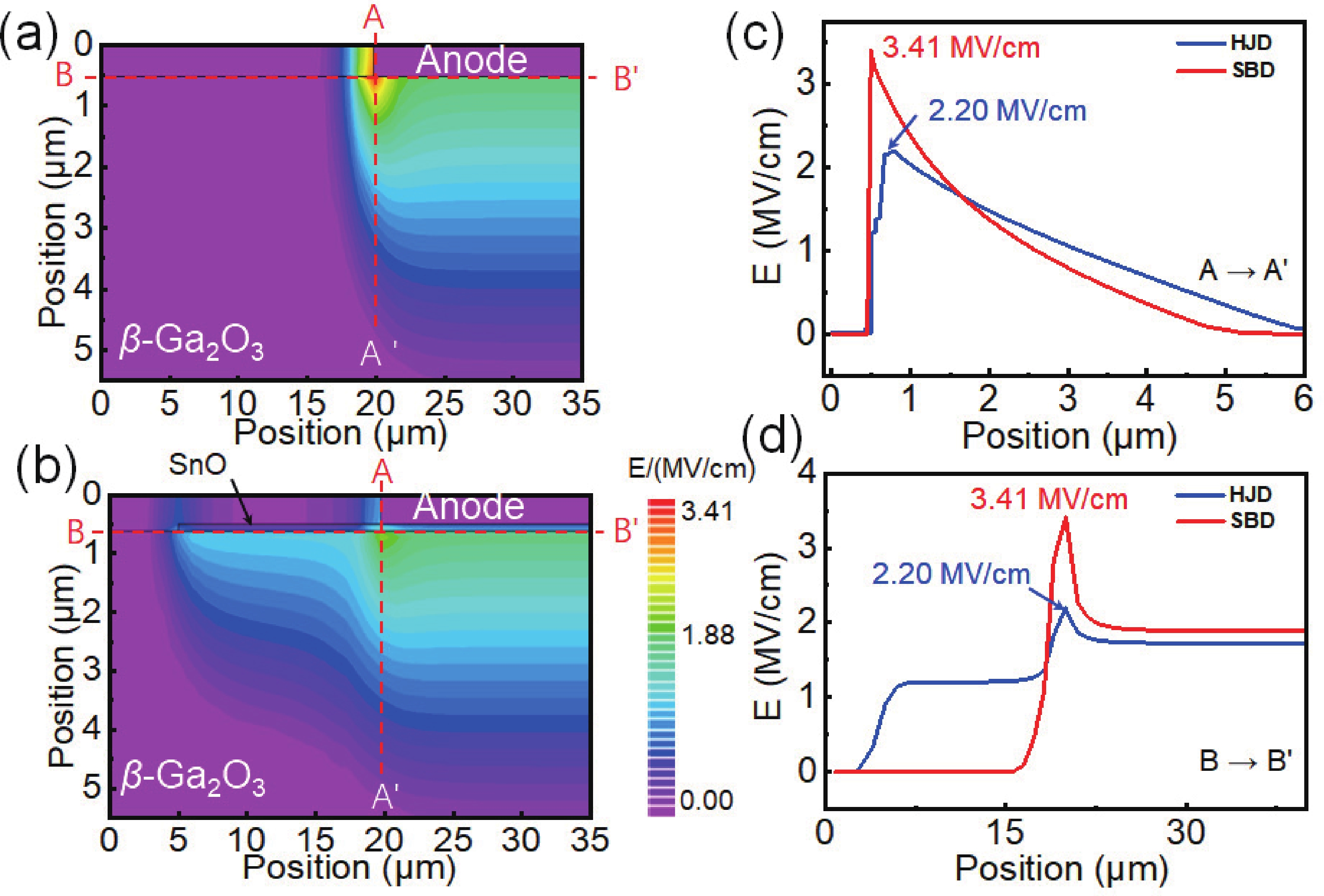
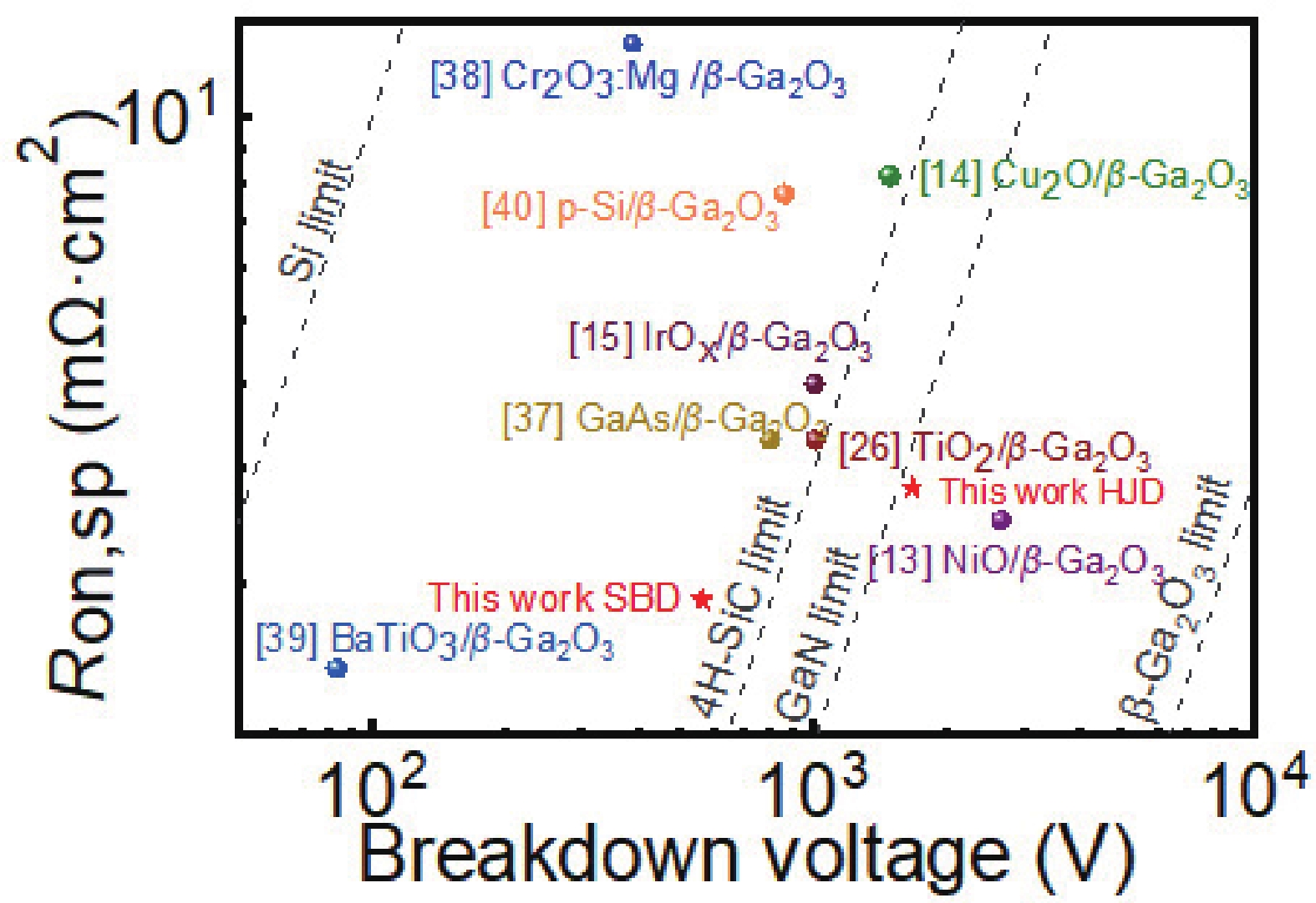
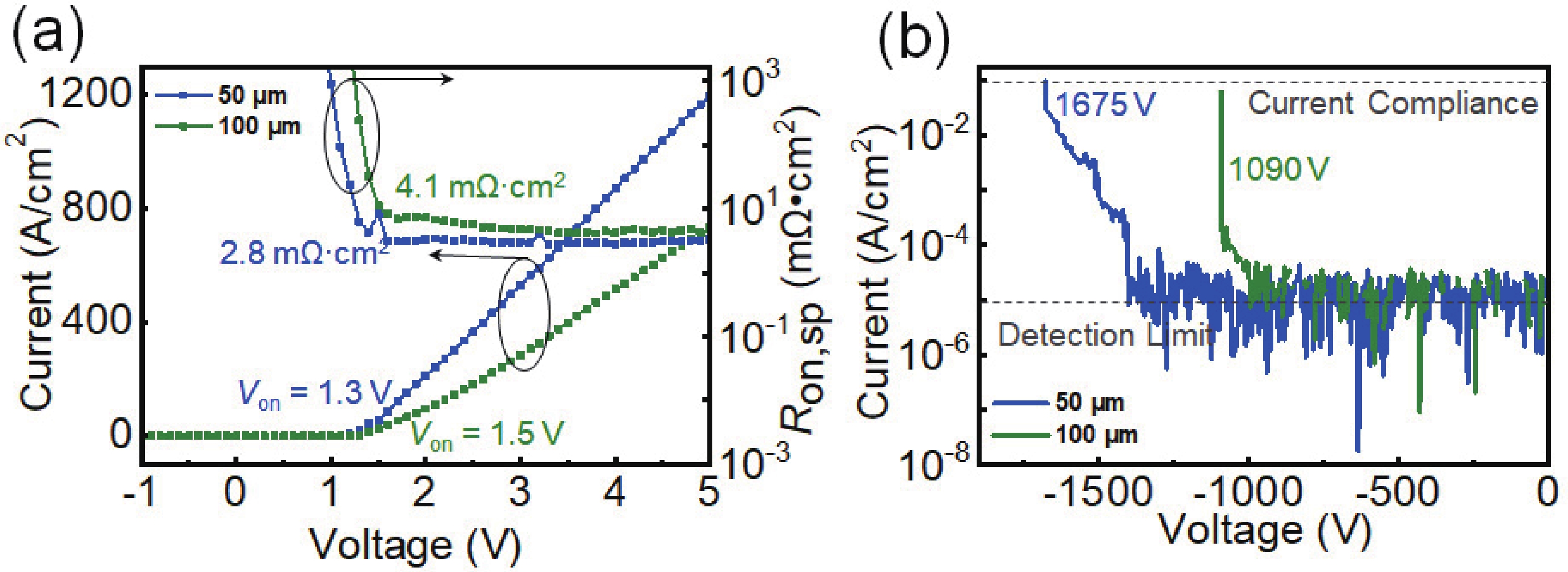
Abstract: In this study, we present the fabrication of vertical SnO/β-Ga2O3 heterojunction diode (HJD) via radio frequency (RF) reactive magnetron sputtering. The valence and conduction band offsets between β-Ga2O3 and SnO are determined to be 2.65 and 0.75 eV, respectively, through X-ray photoelectron spectroscopy, showing a type-Ⅱ band alignment. Compared to its Schottky barrier diode (SBD) counterpart, the HJD presents a comparable specific ON-resistances (Ron,sp) of 2.8 mΩ·cm² and lower reverse leakage current (IR), leading to an enhanced reverse blocking characteristics with breakdown voltage (BV) of 1675 V and power figure of merit (PFOM) of 1.0 GW/cm². This demonstrates the high quality of the SnO/β-Ga2O3 heterojunction interface. Silvaco TCAD simulation further reveals that electric field crowding at the edge of anode for the SBD was greatly depressed by the introduction of SnO film, revealing the potential application of SnO/β-Ga2O3 heterojunction in the future β-Ga2O3-based power devices.
Keywords: band alignment, heterojunction diode (HJD), power semiconductor devices, β-gallium oxide (β-Ga2O3)
| [1] |
Li B T, Zhang X D, Zhang L, et al. A comprehensive review of recent progress on enhancement-mode β-Ga2O3 FETs: Growth, devices and properties. J Semicond, 2023, 44(6), 061801 doi: 10.1088/1674-4926/44/6/061801
|
| [2] |
Kuramata A, Koshi K, Watanabe S, et al. High-quality β-Ga2O3 single crystals grown by edge-defined film-fed growth. Jpn J Appl Phys, 2016, 55(12), 1202A2 doi: 10.7567/JJAP.55.1202A2
|
| [3] |
Galazka Z, Uecker R, Klimm D, et al. Scaling-up of bulk β-Ga2O3 single crystals by the czochralski method. ECS J Solid State Sci Technol, 2017, 6(2), Q3007 doi: 10.1149/2.0021702jss
|
| [4] |
Ji M, Taylor N R, Kravchenko I, et al. Demonstration of large-size vertical Ga2O3 Schottky barrier diodes. IEEE Trans Power Electron, 2021, 36(1), 41 doi: 10.1109/TPEL.2020.3001530
|
| [5] |
Wang Y G, Gong H H, Lv Y J, et al. 2.41 kV vertical p-NiO/n-Ga2O3 heterojunction diodes with a record Baliga’s figure-of-merit of 5.18 GW/cm2. IEEE Trans Power Electron, 2022, 37(4), 3743 doi: 10.1109/TPEL.2021.3123940
|
| [6] |
Li W S, Nomoto K, Hu Z Y, et al. Field-plated Ga2O3 trench Schottky barrier diodes with a BV2/Ron, sp of up to 0.95 GW/cm2. IEEE Electron Device Lett, 2020, 41(1), 107 doi: 10.1109/LED.2019.2953559
|
| [7] |
He Q M, Zhou X Z, Li Q Y, et al. Selective high-resistance zones formed by oxygen annealing for β-Ga2O3 Schottky diode applications. IEEE Electron Device Lett, 2022, 43(11), 1933 doi: 10.1109/LED.2022.3205326
|
| [8] |
Dhara S, Kalarickal K N, Dheenan A, et al. β-Ga2O3 Schottky barrier diodes with 4.1 MV/cm field strength by deep plasma etching field-termination. Appl Phys Lett, 2022, 121(20), 203501 doi: 10.1063/5.0123284
|
| [9] |
Han Z, Jian G Z, Zhou X Z, et al. 2.7 kV low leakage vertical PtOx/β-Ga2O3 Schottky barrier diodes with self-aligned mesa termination. IEEE Electron Device Lett, 2023, 44(10), 1680 doi: 10.1109/LED.2023.3305389
|
| [10] |
Li W S, Saraswat D, Long Y Y, et al. Near-ideal reverse leakage current and practical maximum electric field in β-Ga2O3 Schottky barrier diodes. Appl Phys Lett, 2020, 116(19), 192101 doi: 10.1063/5.0007715
|
| [11] |
Ji X Q, Lu C, Yan Z Y, et al. A review of gallium oxide-based power Schottky barrier diodes. J Phys D: Appl Phys, 2022, 55(44), 443002 doi: 10.1088/1361-6463/ac855c
|
| [12] |
Kokubun Y, Kubo S, Nakagomi S. All-oxide p–n heterojunction diodes comprising p-type NiO and n-type β-Ga2O3. Appl Phys Express, 2016, 9(9), 091101 doi: 10.7567/APEX.9.091101
|
| [13] |
Hao W B, He Q M, Zhou X Z, et al. 2.6 kV NiO/Ga2O3 heterojunction diode with superior high-temperature voltage blocking capability. 2022 IEEE 34th International Symposium on Power Semiconductor Devices and ICs (ISPSD), 2022, 105 doi: 10.1109/ISPSD49238.2022.981368
|
| [14] |
Watahiki T, Yuda Y, Furukawa A, et al. Heterojunction p-Cu2O/n-Ga2O3 diode with high breakdown voltage. Appl Phys Lett, 2017, 111(22), 222104 doi: 10.1063/1.4998311
|
| [15] |
Zheng R T, Feng W Y, Liao C, et al. P-IrOx/n-β-Ga2O3 heterojunction diodes with 1-kV breakdown and ultralow leakage current below 0.1 μA/cm2. IEEE Trans Electron Devices, 2024, 71(3), 1587 doi: 10.1109/TED.2023.3339404
|
| [16] |
Gong H H, Zhou F, Xu W Z, et al. 1.37 kV/12 A NiO/β-Ga2O3 heterojunction diode with nanosecond reverse recovery and rugged surge-current capability. IEEE Trans Power Electron, 2021, 36(11), 12213 doi: 10.1109/TPEL.2021.3082640
|
| [17] |
Zhang J Y, Li W W, Hoye R L Z, et al. Electronic and transport properties of Li-doped NiO epitaxial thin films. J Mater Chem C, 2018, 6(9), 2275 doi: 10.1039/C7TC05331B
|
| [18] |
Budde M, Mazzolini P, Feldl J, et al. Plasma-assisted molecular beam epitaxy of SnO (001) films: Metastability, hole transport properties, Seebeck coefficient, and effective hole mass. Phys Rev Materials, 2020, 4(12), 124602 doi: 10.1103/PhysRevMaterials.4.124602
|
| [19] |
Zeng Y, Huang H, Zhao X L, et al. Self-powered a-SnOx/c-Ga2O3 pn heterojunction solar-blind photodetector with high responsivity and swift response speed. IEEE Electron Device Lett, 2023, 44(12), 2003 doi: 10.1109/LED.2023.3325228
|
| [20] |
Budde M, Splith D, Mazzolini P, et al. SnO/β-Ga2O3 vertical pn heterojunction diodes. Appl Phys Lett, 2020, 117(25), 252106 doi: 10.1063/5.0031442
|
| [21] |
Yang J C, Sparks Z, Ren F, et al. Effect of surface treatments on electrical properties of β-Ga2O3. J Vac Sci Technol B, 2018, 36(6), 061201 doi: 10.1116/1.5052229
|
| [22] |
Huan Y W, Sun S M, Gu C J, et al. Recent advances in β-Ga2O3-metal contacts. Nanoscale Res Lett, 2018, 13(1), 246 doi: 10.1186/s11671-018-2667-2
|
| [23] |
Lee M H, Chou T S, Bin Anooz S, et al. Effect of post-metallization anneal on (100) Ga2O3/Ti–Au ohmic contact performance and interfacial degradation. APL Materials, 2022, 10(9), 091105 doi: 10.1063/5.0096245
|
| [24] |
Luo H, Liang L Y, Cao H T, et al. Structural, chemical, optical, and electrical evolution of SnOx films deposited by reactive rf magnetron sputtering. ACS Appl Mater Interfaces, 2012, 4(10), 5673 doi: 10.1021/am301601s
|
| [25] |
Kamimura T, Sasaki K, Hoi Wong M, et al. Band alignment and electrical properties of Al2O3/β-Ga2O3 heterojunctions. Appl Phys Lett, 2014, 104(19), 192104 doi: 10.1063/1.4876920
|
| [26] |
Zhou F, Gong H H, Xu W Z, et al. 1.95-kV Beveled-Mesa NiO/β-Ga2O3 heterojunction diode with 98.5% conversion efficiency and over million-times overvoltage ruggedness. IEEE Trans Power Electron, 2022, 37(2), 1223 doi: 10.1109/TPEL.2021.3108780
|
| [27] |
Hu Z Z, Li J G, Zhao C Y, et al. Design and fabrication of vertical metal/TiO2/β-Ga2O3 dielectric heterojunction diode with reverse blocking voltage of 1010 V. IEEE Trans Electron Devices, 2020, 67(12), 5628 doi: 10.1109/TED.2020.3033787
|
| [28] |
Deng Y X, Yang Z Q, Xu T L, et al. Band alignment and electrical properties of NiO/β-Ga2O3 heterojunctions with different β-Ga2O3 orientations. Appl Surf Sci, 2023, 622, 156917 doi: 10.1016/j.apsusc.2023.156917
|
| [29] |
Gong H H, Chen X H, Xu Y, et al. A 1.86-kV double-layered NiO/β-Ga2O3 vertical p–n heterojunction diode. Appl Phys Lett, 2020, 117(2), 022104 doi: 10.1063/5.0010052
|
| [30] |
Luo H X, Zhou X D, Chen Z M, et al. Fabrication and characterization of high-voltage NiO/β- Ga2O3 heterojunction power diodes. IEEE Trans Electron Devices, 2021, 68(8), 3991 doi: 10.1109/TED.2021.3091548
|
| [31] |
Gong H H, Chen X H, Xu Y, et al. Band alignment and interface recombination in NiO/β-Ga2O3 type-Ⅱ p−n heterojunctions. IEEE Trans Electron Devices, 2020, 67(8), 3341 doi: 10.1109/TED.2020.3001249
|
| [32] |
Li J S, Xia X Y, Chiang C C, et al. Deposition of sputtered NiO as a p-type layer for heterojunction diodes with Ga2O3. J Vac Sci Technol A, 2023, 41(1), 013405 doi: 10.1116/6.0002250
|
| [33] |
Gong H H, Yu X X, Xu Y, et al. β-Ga2O3 vertical heterojunction barrier Schottky diodes terminated with p-NiO field limiting rings. Appl Phys Lett, 2021, 118(20), 202102 doi: 10.1063/5.0050919
|
| [34] |
Hu H D, Feng Z, Wang Y B, et al. The role of surface pretreatment by low temperature O2 gas annealing for β-Ga2O3 Schottky barrier diodes. Appl Phys Lett, 2022, 120(7), 073501 doi: 10.1063/5.0080343
|
| [35] |
Hao W B, He Q M, Zhou K, et al. Low defect density and small I−V curve hysteresis in NiO/β-Ga2O3 pn diode with a high PFOM of 0.65 GW/cm2. Appl Phys Lett, 2021, 118(4), 043501 doi: 10.1063/5.0038349
|
| [36] |
Hao W B, He Q M, Han Z, et al. 1 kV vertical β-Ga2O3 heterojunction barrier Schottky diode with hybrid unipolar and bipolar operation. 2023 35th International Symposium on Power Semiconductor Devices and ICs (ISPSD), 2023, 394 doi: 10.1109/ISPSD57135.2023.10147686
|
| [37] |
Li J S, Chiang C C, Xia X Y, et al. Demonstration of 4.7 kV breakdown voltage in NiO/β-Ga2O3 vertical rectifiers. Appl Phys Lett, 2022, 121(4), 042105 doi: 10.1063/5.0097564
|
| [38] |
Xie S W, Sheikhi M, Xu S N, et al. P-GaAs/n-Ga2O3 heterojunction diode with breakdown voltage of ~800 V. Appl Phys Lett, 2024, 124(7), 073503 doi: 10.1063/5.0181056
|
| [39] |
Callahan W A, Egbo K, Lee C W, et al. Reliable operation of Cr2O3: Mg/β-Ga2O3 p–n heterojunction diodes at 600 °C. Appl Phys Lett, 2024, 124(15), 153504 doi: 10.1063/5.0185566
|
| [40] |
Xia Z B, Chandrasekar H, Moore W, et al. Metal/BaTiO3/β-Ga2O3 dielectric heterojunction diode with 5.7 MV/cm breakdown field. Appl Phys Lett, 2019, 115(25), 252104 doi: 10.1063/1.5130669
|
| [41] |
Xie S W, Alam M T, Gong J R, et al. 0.86 kV p-Si/(001)-Ga2O3 heterojunction diode. IEEE Electron Device Lett, 2024, 45(3), 444 doi: 10.1109/LED.2024.3352515
|


Article views: 1837 Times PDF downloads: 186 Times Cited by: 0 Times
Received: 13 February 2025 Revised: 11 March 2025 Online: Accepted Manuscript: 27 March 2025Uncorrected proof: 28 April 2025Published: 01 August 2025
| Citation: |
Xia Wu, Chenyang Huang, Xiuxing Xu, Jun Wang, Xinwang Yao, Yanfang Liu, Xiujuan Wang, Chunyan Wu, Linbao Luo. Band alignment of SnO/β-Ga2O3 heterojunction and its electrical properties for power device application[J]. Journal of Semiconductors, 2025, 46(8): 082503. doi: 10.1088/1674-4926/25020008
****
X Wu, C Y Huang, X X Xu, J Wang, X W Yao, Y F Liu, X J Wang, C Y Wu, and L B Luo, Band alignment of SnO/β-Ga2O3 heterojunction and its electrical properties for power device application[J]. J. Semicond., 2025, 46(8), 082503 doi: 10.1088/1674-4926/25020008

|
 Xia Wu received her bachelor’s degree from Chizhou University in 2020. Currently, she is a master’s student at Hefei University of Technology under the supervision of Prof. Chunyan Wu. Her research focuses on power diode devices based on β-Ga2O3
 Chunyan Wu received her Ph.D. degree in inorganic chemistry from the University of Science and Technology of China in 2006. She is currently a professor at the School of Microlectronics, Hefei University of Technology, China. Her research interest mainly focuses on high-performance optoelectronic and electronic device applications, including photodetectors, optoelectronic synaptic devices and power devices
| [1] |
Li B T, Zhang X D, Zhang L, et al. A comprehensive review of recent progress on enhancement-mode β-Ga2O3 FETs: Growth, devices and properties. J Semicond, 2023, 44(6), 061801 doi: 10.1088/1674-4926/44/6/061801
|
| [2] |
Kuramata A, Koshi K, Watanabe S, et al. High-quality β-Ga2O3 single crystals grown by edge-defined film-fed growth. Jpn J Appl Phys, 2016, 55(12), 1202A2 doi: 10.7567/JJAP.55.1202A2
|
| [3] |
Galazka Z, Uecker R, Klimm D, et al. Scaling-up of bulk β-Ga2O3 single crystals by the czochralski method. ECS J Solid State Sci Technol, 2017, 6(2), Q3007 doi: 10.1149/2.0021702jss
|
| [4] |
Ji M, Taylor N R, Kravchenko I, et al. Demonstration of large-size vertical Ga2O3 Schottky barrier diodes. IEEE Trans Power Electron, 2021, 36(1), 41 doi: 10.1109/TPEL.2020.3001530
|
| [5] |
Wang Y G, Gong H H, Lv Y J, et al. 2.41 kV vertical p-NiO/n-Ga2O3 heterojunction diodes with a record Baliga’s figure-of-merit of 5.18 GW/cm2. IEEE Trans Power Electron, 2022, 37(4), 3743 doi: 10.1109/TPEL.2021.3123940
|
| [6] |
Li W S, Nomoto K, Hu Z Y, et al. Field-plated Ga2O3 trench Schottky barrier diodes with a BV2/Ron, sp of up to 0.95 GW/cm2. IEEE Electron Device Lett, 2020, 41(1), 107 doi: 10.1109/LED.2019.2953559
|
| [7] |
He Q M, Zhou X Z, Li Q Y, et al. Selective high-resistance zones formed by oxygen annealing for β-Ga2O3 Schottky diode applications. IEEE Electron Device Lett, 2022, 43(11), 1933 doi: 10.1109/LED.2022.3205326
|
| [8] |
Dhara S, Kalarickal K N, Dheenan A, et al. β-Ga2O3 Schottky barrier diodes with 4.1 MV/cm field strength by deep plasma etching field-termination. Appl Phys Lett, 2022, 121(20), 203501 doi: 10.1063/5.0123284
|
| [9] |
Han Z, Jian G Z, Zhou X Z, et al. 2.7 kV low leakage vertical PtOx/β-Ga2O3 Schottky barrier diodes with self-aligned mesa termination. IEEE Electron Device Lett, 2023, 44(10), 1680 doi: 10.1109/LED.2023.3305389
|
| [10] |
Li W S, Saraswat D, Long Y Y, et al. Near-ideal reverse leakage current and practical maximum electric field in β-Ga2O3 Schottky barrier diodes. Appl Phys Lett, 2020, 116(19), 192101 doi: 10.1063/5.0007715
|
| [11] |
Ji X Q, Lu C, Yan Z Y, et al. A review of gallium oxide-based power Schottky barrier diodes. J Phys D: Appl Phys, 2022, 55(44), 443002 doi: 10.1088/1361-6463/ac855c
|
| [12] |
Kokubun Y, Kubo S, Nakagomi S. All-oxide p–n heterojunction diodes comprising p-type NiO and n-type β-Ga2O3. Appl Phys Express, 2016, 9(9), 091101 doi: 10.7567/APEX.9.091101
|
| [13] |
Hao W B, He Q M, Zhou X Z, et al. 2.6 kV NiO/Ga2O3 heterojunction diode with superior high-temperature voltage blocking capability. 2022 IEEE 34th International Symposium on Power Semiconductor Devices and ICs (ISPSD), 2022, 105 doi: 10.1109/ISPSD49238.2022.981368
|
| [14] |
Watahiki T, Yuda Y, Furukawa A, et al. Heterojunction p-Cu2O/n-Ga2O3 diode with high breakdown voltage. Appl Phys Lett, 2017, 111(22), 222104 doi: 10.1063/1.4998311
|
| [15] |
Zheng R T, Feng W Y, Liao C, et al. P-IrOx/n-β-Ga2O3 heterojunction diodes with 1-kV breakdown and ultralow leakage current below 0.1 μA/cm2. IEEE Trans Electron Devices, 2024, 71(3), 1587 doi: 10.1109/TED.2023.3339404
|
| [16] |
Gong H H, Zhou F, Xu W Z, et al. 1.37 kV/12 A NiO/β-Ga2O3 heterojunction diode with nanosecond reverse recovery and rugged surge-current capability. IEEE Trans Power Electron, 2021, 36(11), 12213 doi: 10.1109/TPEL.2021.3082640
|
| [17] |
Zhang J Y, Li W W, Hoye R L Z, et al. Electronic and transport properties of Li-doped NiO epitaxial thin films. J Mater Chem C, 2018, 6(9), 2275 doi: 10.1039/C7TC05331B
|
| [18] |
Budde M, Mazzolini P, Feldl J, et al. Plasma-assisted molecular beam epitaxy of SnO (001) films: Metastability, hole transport properties, Seebeck coefficient, and effective hole mass. Phys Rev Materials, 2020, 4(12), 124602 doi: 10.1103/PhysRevMaterials.4.124602
|
| [19] |
Zeng Y, Huang H, Zhao X L, et al. Self-powered a-SnOx/c-Ga2O3 pn heterojunction solar-blind photodetector with high responsivity and swift response speed. IEEE Electron Device Lett, 2023, 44(12), 2003 doi: 10.1109/LED.2023.3325228
|
| [20] |
Budde M, Splith D, Mazzolini P, et al. SnO/β-Ga2O3 vertical pn heterojunction diodes. Appl Phys Lett, 2020, 117(25), 252106 doi: 10.1063/5.0031442
|
| [21] |
Yang J C, Sparks Z, Ren F, et al. Effect of surface treatments on electrical properties of β-Ga2O3. J Vac Sci Technol B, 2018, 36(6), 061201 doi: 10.1116/1.5052229
|
| [22] |
Huan Y W, Sun S M, Gu C J, et al. Recent advances in β-Ga2O3-metal contacts. Nanoscale Res Lett, 2018, 13(1), 246 doi: 10.1186/s11671-018-2667-2
|
| [23] |
Lee M H, Chou T S, Bin Anooz S, et al. Effect of post-metallization anneal on (100) Ga2O3/Ti–Au ohmic contact performance and interfacial degradation. APL Materials, 2022, 10(9), 091105 doi: 10.1063/5.0096245
|
| [24] |
Luo H, Liang L Y, Cao H T, et al. Structural, chemical, optical, and electrical evolution of SnOx films deposited by reactive rf magnetron sputtering. ACS Appl Mater Interfaces, 2012, 4(10), 5673 doi: 10.1021/am301601s
|
| [25] |
Kamimura T, Sasaki K, Hoi Wong M, et al. Band alignment and electrical properties of Al2O3/β-Ga2O3 heterojunctions. Appl Phys Lett, 2014, 104(19), 192104 doi: 10.1063/1.4876920
|
| [26] |
Zhou F, Gong H H, Xu W Z, et al. 1.95-kV Beveled-Mesa NiO/β-Ga2O3 heterojunction diode with 98.5% conversion efficiency and over million-times overvoltage ruggedness. IEEE Trans Power Electron, 2022, 37(2), 1223 doi: 10.1109/TPEL.2021.3108780
|
| [27] |
Hu Z Z, Li J G, Zhao C Y, et al. Design and fabrication of vertical metal/TiO2/β-Ga2O3 dielectric heterojunction diode with reverse blocking voltage of 1010 V. IEEE Trans Electron Devices, 2020, 67(12), 5628 doi: 10.1109/TED.2020.3033787
|
| [28] |
Deng Y X, Yang Z Q, Xu T L, et al. Band alignment and electrical properties of NiO/β-Ga2O3 heterojunctions with different β-Ga2O3 orientations. Appl Surf Sci, 2023, 622, 156917 doi: 10.1016/j.apsusc.2023.156917
|
| [29] |
Gong H H, Chen X H, Xu Y, et al. A 1.86-kV double-layered NiO/β-Ga2O3 vertical p–n heterojunction diode. Appl Phys Lett, 2020, 117(2), 022104 doi: 10.1063/5.0010052
|
| [30] |
Luo H X, Zhou X D, Chen Z M, et al. Fabrication and characterization of high-voltage NiO/β- Ga2O3 heterojunction power diodes. IEEE Trans Electron Devices, 2021, 68(8), 3991 doi: 10.1109/TED.2021.3091548
|
| [31] |
Gong H H, Chen X H, Xu Y, et al. Band alignment and interface recombination in NiO/β-Ga2O3 type-Ⅱ p−n heterojunctions. IEEE Trans Electron Devices, 2020, 67(8), 3341 doi: 10.1109/TED.2020.3001249
|
| [32] |
Li J S, Xia X Y, Chiang C C, et al. Deposition of sputtered NiO as a p-type layer for heterojunction diodes with Ga2O3. J Vac Sci Technol A, 2023, 41(1), 013405 doi: 10.1116/6.0002250
|
| [33] |
Gong H H, Yu X X, Xu Y, et al. β-Ga2O3 vertical heterojunction barrier Schottky diodes terminated with p-NiO field limiting rings. Appl Phys Lett, 2021, 118(20), 202102 doi: 10.1063/5.0050919
|
| [34] |
Hu H D, Feng Z, Wang Y B, et al. The role of surface pretreatment by low temperature O2 gas annealing for β-Ga2O3 Schottky barrier diodes. Appl Phys Lett, 2022, 120(7), 073501 doi: 10.1063/5.0080343
|
| [35] |
Hao W B, He Q M, Zhou K, et al. Low defect density and small I−V curve hysteresis in NiO/β-Ga2O3 pn diode with a high PFOM of 0.65 GW/cm2. Appl Phys Lett, 2021, 118(4), 043501 doi: 10.1063/5.0038349
|
| [36] |
Hao W B, He Q M, Han Z, et al. 1 kV vertical β-Ga2O3 heterojunction barrier Schottky diode with hybrid unipolar and bipolar operation. 2023 35th International Symposium on Power Semiconductor Devices and ICs (ISPSD), 2023, 394 doi: 10.1109/ISPSD57135.2023.10147686
|
| [37] |
Li J S, Chiang C C, Xia X Y, et al. Demonstration of 4.7 kV breakdown voltage in NiO/β-Ga2O3 vertical rectifiers. Appl Phys Lett, 2022, 121(4), 042105 doi: 10.1063/5.0097564
|
| [38] |
Xie S W, Sheikhi M, Xu S N, et al. P-GaAs/n-Ga2O3 heterojunction diode with breakdown voltage of ~800 V. Appl Phys Lett, 2024, 124(7), 073503 doi: 10.1063/5.0181056
|
| [39] |
Callahan W A, Egbo K, Lee C W, et al. Reliable operation of Cr2O3: Mg/β-Ga2O3 p–n heterojunction diodes at 600 °C. Appl Phys Lett, 2024, 124(15), 153504 doi: 10.1063/5.0185566
|
| [40] |
Xia Z B, Chandrasekar H, Moore W, et al. Metal/BaTiO3/β-Ga2O3 dielectric heterojunction diode with 5.7 MV/cm breakdown field. Appl Phys Lett, 2019, 115(25), 252104 doi: 10.1063/1.5130669
|
| [41] |
Xie S W, Alam M T, Gong J R, et al. 0.86 kV p-Si/(001)-Ga2O3 heterojunction diode. IEEE Electron Device Lett, 2024, 45(3), 444 doi: 10.1109/LED.2024.3352515
|

 WeChat ID
Journal of Semiconductors © 2017 All Rights Reserved 京ICP备05085259号-2

 DownLoad:

