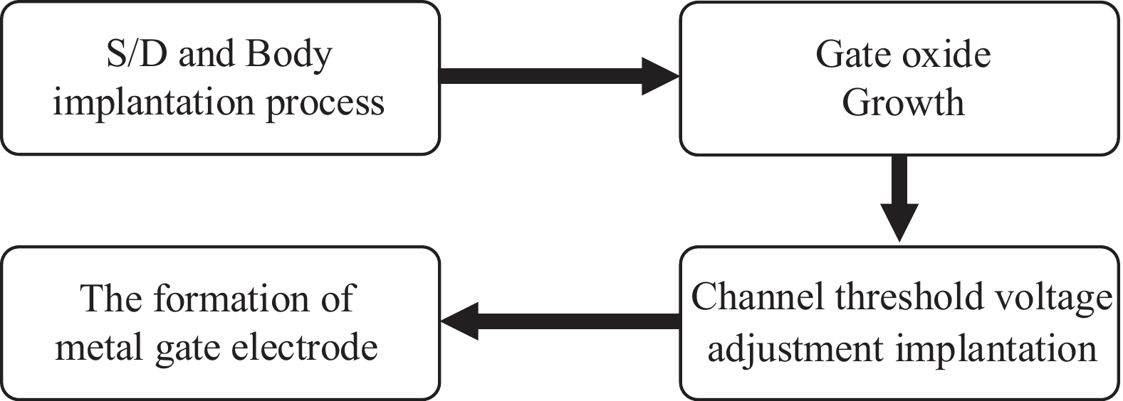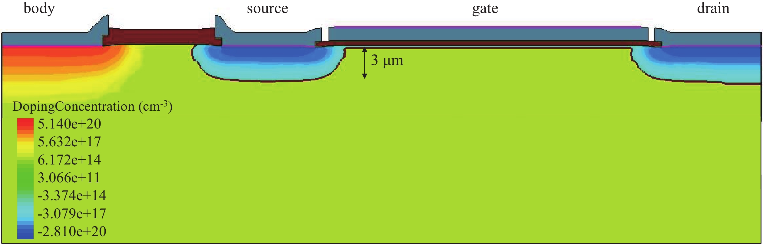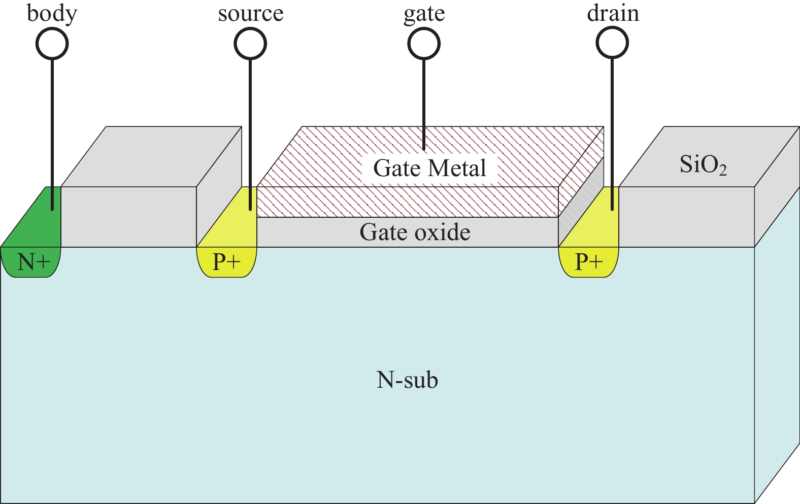
Fig. 1.
(Color online) The structure of PMOS transistor.
ARTICLES
Jun Huang, Bojin Pan, Hang bao, Qiuyue Huo, Renxiong Li, Qi Ding, Yutuo Guo, Yu Wang, Kunqin He, Yaxin Liu, Ziyi Zeng, Ning Ning and Lulu Peng
Corresponding author: Lulu Peng, lulu.peng@cumec.cn
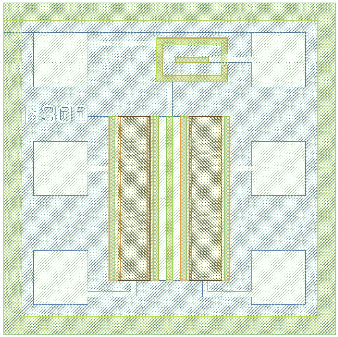
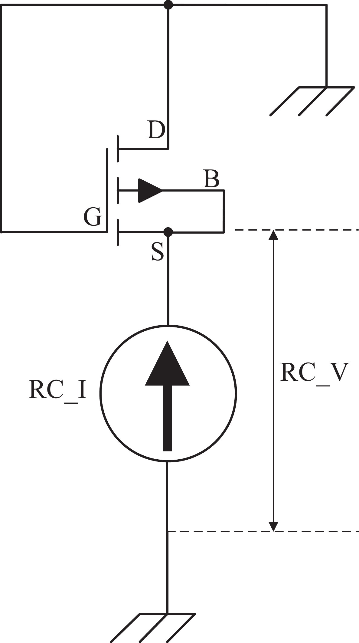
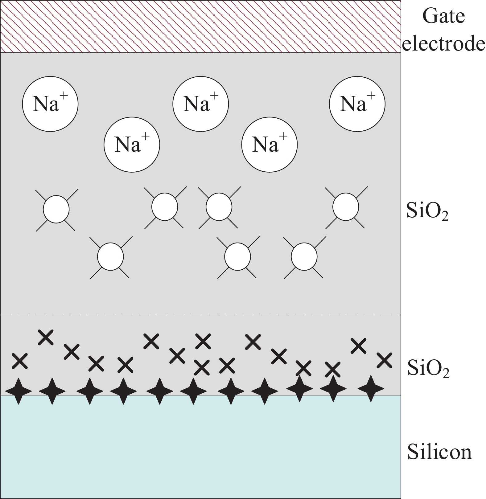
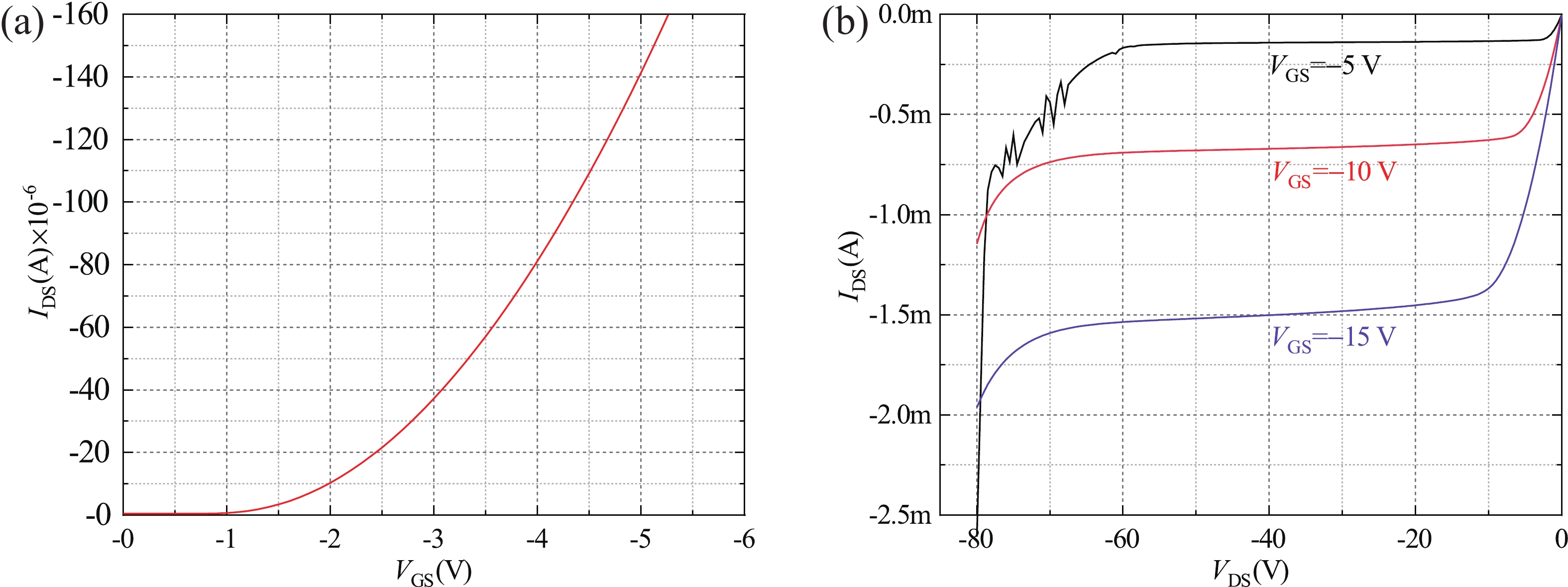
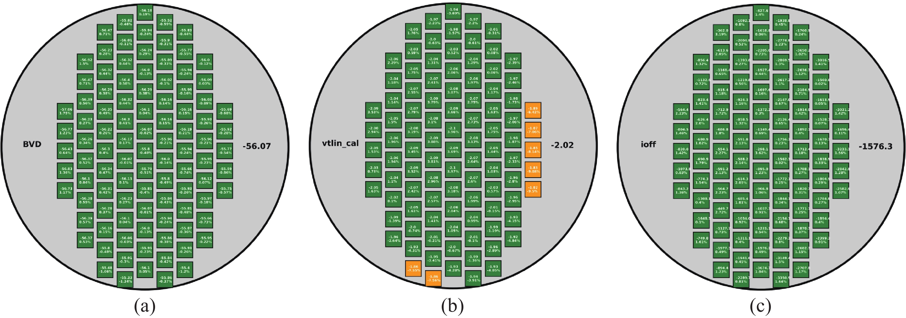
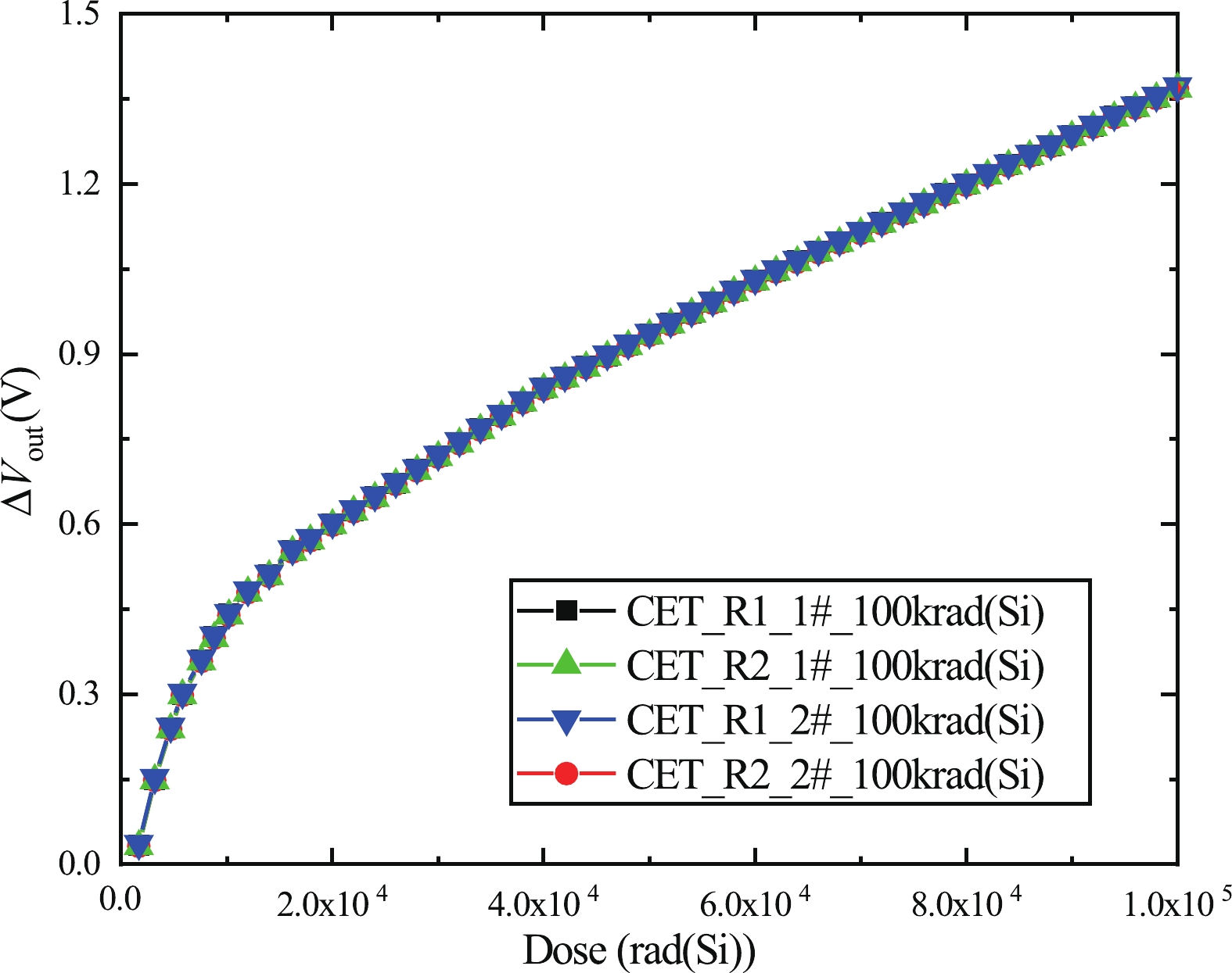
Abstract: The radiation-sensitive field effect transistors (RADFET) radiation dosimeter is a type of radiation detector based on the total dose effects of the p-channel metal−oxide−semiconductor (PMOS) transistor. The RADFET chip was fabricated in United Microelectronics Center 8-inch process with a six-layer photomask. The chip including two identical PMOS transistors, occupies a size of 610 µm × 610 µm. Each PMOS has a W/L ratio of 300 µm/50 µm, and a 400 nm thick gate oxide, which is formed by a dry-wet-dry oxygen process. The wet oxygen-formed gate oxide with more traps can capture more holes during irradiation, thus significantly changing the PMOS threshold voltage. Pre-irradiation measurement results from ten test chips show that the initial average voltage of the PMOS is 1.961 V with a dispersion of 5.7%. The irradiation experiment is conducted in a cobalt source facility with a dose rate of 50 rad(Si)/s. During irradiation, a constant current source circuit of 10 µA was connected to monitoring the shift in threshold voltage under different total dose. When the total dose is 100 krad(Si), the shift in threshold voltage was approximately 1.37 V, which demonstrates that an excellent radiation function was achieved.
Keywords: RADFET, PMOS, thick gate oxide, total dose effect, radiation detection
| [1] |
Holmes-Siedle A, Adams L. RADFET: A review of the use of metal-oxide-silicon devices as integrating dosimeters. Radiat Phys Chem, 1986, 28(2), 235 doi: 10.1016/1359-0197(86)90134-7
|
| [2] |
Karmakar A, Wang J L, Prinzie J, et al. A review of semiconductor based ionising radiation sensors used in harsh radiation environments and their applications. Radiation, 2021, 1(3), 194 doi: 10.3390/radiation1030018
|
| [3] |
Pejović S M, Pejović M M, Živanović M. Small dose effect in RADFET with thick gate oxide. Appl Radiat Isot, 2019, 152, 72 doi: 10.1016/j.apradiso.2019.06.034
|
| [4] |
Morozzi A, Moscatelli F, Croci T, et al. TCAD modeling of surface radiation damage effects: A state-of-the-art review. Front Phys, 2021, 9, 617322 doi: 10.3389/fphy.2021.617322
|
| [5] |
Pejović M M, Pejović S M. P-channel MOSFET as ionizing radiation detector. Appl Radiat Isot, 2023, 196, 110730 doi: 10.1016/j.apradiso.2023.110730
|
| [6] |
Andjelkovic M, Simevski A, Chen J C, et al. A design concept for radiation hardened RADFET readout system for space applications. Microprocess Microsyst, 2022, 90, 104486 doi: 10.1016/j.micpro.2022.104486
|
| [7] |
Andjelkovic M, Simevski A, Chen J C, et al. Design of radiation hardened RADFET readout system for space applications. 2020 23rd Euromicro Conference on Digital System Design (DSD), 2020, 484 doi: 10.1109/DSD51259.2020.00082
|
| [8] |
Ullah S. A fully integrated rad FET dosimeter for radiation measurement in space. Proceedings of the 2021 International Conference on Artificial Intelligence in Electronics Engineering (ICAIEE), 2021, 225 doi: 10.1145/3461890.3461899
|
| [9] |
Elfiky D, Abd-Rabou A S, Akah H, et al. Development and fabrication of MOSFET-based radiation dosimeter (RadFET) for enhanced performance in space missions. J Adv Res Appl Sci Eng Technol, 2024, 39(1), 135 doi: 10.37934/araset.39.1.135148
|
| [10] |
Ruiz-García I, Martín-Holgado P, Escobedo P, et al. Temperature effects on the sensitivity of gamma MOSFET dosimeters. 2023 IEEE 33rd International Conference on Microelectronics (MIEL), 2023, 1 doi: 10.1109/MIEL58498.2023.10315922
|
| [11] |
Zhang T Y, Hong Y, Li J Y, et al. Radiation hardened MOSFETs realized by Al2O3 induced Bi-GdF3 with trapped interfacial electrons located in Ti3C2T framework. Compos Sci Technol, 2024, 258, 110911 doi: 10.1016/j.compscitech.2024.110911
|
| [12] |
Kulhar M, Dhoot K, Pandya A. Gamma dose rate measurement using RadFET. IEEE Trans Nucl Sci, 2019, 66(10), 2220 doi: 10.1109/TNS.2019.2942955
|
| [13] |
Andreev D V. Accumulation and erase of radiation-induced charge in MOS structures. Poverhnost, 2024, 6(93), 93 doi: 10.31857/S1028096024060137
|
| [14] |
Andreev D V. Accumulation and suppression of radiation-induced charge in MOS structures. J Surf Investig X Ray Synchrotron Neutron Tech, 2024, 18(2), 461 doi: 10.1134/S102745102402023X
|
| [15] |
Ristic G S, Ilic S D, Andjelkovic M S, et al. Sensitivity and fading of irradiated RADFETs with different gate voltages. Nucl Instrum Meth Phys Res Sect A Accel Spectrometers Detect Assoc Equip, 2022, 1029, 166473 doi: 10.1016/j.nima.2022.166473
|
| [16] |
Ristic G S, Ilic S D, Duane R, et al. Radiation sensitive MOSFETs irradiated with various positive gate biases. J Radiat Res Appl Sci, 2021, 14(1), 353 doi: 10.1080/16878507.2021.1970921
|
| [17] |
Liu H R, Wang S M, Zhang J W. The effect of the boron-ions implantation on the performance of RADFETs. Sci China Technol Sci, 2016, 59(11), 1785 doi: 10.1007/s11431-016-0062-3
|


Article views: 1610 Times PDF downloads: 119 Times Cited by: 0 Times
Received: 19 December 2024 Revised: 28 February 2025 Online: Uncorrected proof: 27 March 2025Published: 01 August 2025
| Citation: |
Jun Huang, Bojin Pan, Hang bao, Qiuyue Huo, Renxiong Li, Qi Ding, Yutuo Guo, Yu Wang, Kunqin He, Yaxin Liu, Ziyi Zeng, Ning Ning, Lulu Peng. A semiconductor radiation dosimeter fabricated in 8-inch process[J]. Journal of Semiconductors, 2025, 46(8): 082302. doi: 10.1088/1674-4926/24120027
****
J Huang, B J Pan, H bao, Q Y Huo, R X Li, Q Ding, Y T Guo, Y Wang, K Q He, Y X Liu, Z Y Zeng, N Ning, and L L Peng, A semiconductor radiation dosimeter fabricated in 8-inch process[J]. J. Semicond., 2025, 46(8), 082302 doi: 10.1088/1674-4926/24120027

|
 Jun Huang received his Ph.D. degree from University of Electronic Science and Technology of China, Chengdu, China, in 2019. He is currently a senior engineer of United Microelectronics Center Co., Ltd, Chongqing, China. His works include power devices and driver IC
 Lulu Peng received his Ph.D. degree in the Hong Kong University of Science and Technology, Hong Kong, China, in 2014. After that, he worked as a Member of Technical Staff in Globalfoundries, Singapore until 2022. He is currently a Chief Expert in the United Microelectronics Center of CETC, Chongqing, China. His current research focuses on Si-based integrated power devices and process for system-on-chip (SOC)
| [1] |
Holmes-Siedle A, Adams L. RADFET: A review of the use of metal-oxide-silicon devices as integrating dosimeters. Radiat Phys Chem, 1986, 28(2), 235 doi: 10.1016/1359-0197(86)90134-7
|
| [2] |
Karmakar A, Wang J L, Prinzie J, et al. A review of semiconductor based ionising radiation sensors used in harsh radiation environments and their applications. Radiation, 2021, 1(3), 194 doi: 10.3390/radiation1030018
|
| [3] |
Pejović S M, Pejović M M, Živanović M. Small dose effect in RADFET with thick gate oxide. Appl Radiat Isot, 2019, 152, 72 doi: 10.1016/j.apradiso.2019.06.034
|
| [4] |
Morozzi A, Moscatelli F, Croci T, et al. TCAD modeling of surface radiation damage effects: A state-of-the-art review. Front Phys, 2021, 9, 617322 doi: 10.3389/fphy.2021.617322
|
| [5] |
Pejović M M, Pejović S M. P-channel MOSFET as ionizing radiation detector. Appl Radiat Isot, 2023, 196, 110730 doi: 10.1016/j.apradiso.2023.110730
|
| [6] |
Andjelkovic M, Simevski A, Chen J C, et al. A design concept for radiation hardened RADFET readout system for space applications. Microprocess Microsyst, 2022, 90, 104486 doi: 10.1016/j.micpro.2022.104486
|
| [7] |
Andjelkovic M, Simevski A, Chen J C, et al. Design of radiation hardened RADFET readout system for space applications. 2020 23rd Euromicro Conference on Digital System Design (DSD), 2020, 484 doi: 10.1109/DSD51259.2020.00082
|
| [8] |
Ullah S. A fully integrated rad FET dosimeter for radiation measurement in space. Proceedings of the 2021 International Conference on Artificial Intelligence in Electronics Engineering (ICAIEE), 2021, 225 doi: 10.1145/3461890.3461899
|
| [9] |
Elfiky D, Abd-Rabou A S, Akah H, et al. Development and fabrication of MOSFET-based radiation dosimeter (RadFET) for enhanced performance in space missions. J Adv Res Appl Sci Eng Technol, 2024, 39(1), 135 doi: 10.37934/araset.39.1.135148
|
| [10] |
Ruiz-García I, Martín-Holgado P, Escobedo P, et al. Temperature effects on the sensitivity of gamma MOSFET dosimeters. 2023 IEEE 33rd International Conference on Microelectronics (MIEL), 2023, 1 doi: 10.1109/MIEL58498.2023.10315922
|
| [11] |
Zhang T Y, Hong Y, Li J Y, et al. Radiation hardened MOSFETs realized by Al2O3 induced Bi-GdF3 with trapped interfacial electrons located in Ti3C2T framework. Compos Sci Technol, 2024, 258, 110911 doi: 10.1016/j.compscitech.2024.110911
|
| [12] |
Kulhar M, Dhoot K, Pandya A. Gamma dose rate measurement using RadFET. IEEE Trans Nucl Sci, 2019, 66(10), 2220 doi: 10.1109/TNS.2019.2942955
|
| [13] |
Andreev D V. Accumulation and erase of radiation-induced charge in MOS structures. Poverhnost, 2024, 6(93), 93 doi: 10.31857/S1028096024060137
|
| [14] |
Andreev D V. Accumulation and suppression of radiation-induced charge in MOS structures. J Surf Investig X Ray Synchrotron Neutron Tech, 2024, 18(2), 461 doi: 10.1134/S102745102402023X
|
| [15] |
Ristic G S, Ilic S D, Andjelkovic M S, et al. Sensitivity and fading of irradiated RADFETs with different gate voltages. Nucl Instrum Meth Phys Res Sect A Accel Spectrometers Detect Assoc Equip, 2022, 1029, 166473 doi: 10.1016/j.nima.2022.166473
|
| [16] |
Ristic G S, Ilic S D, Duane R, et al. Radiation sensitive MOSFETs irradiated with various positive gate biases. J Radiat Res Appl Sci, 2021, 14(1), 353 doi: 10.1080/16878507.2021.1970921
|
| [17] |
Liu H R, Wang S M, Zhang J W. The effect of the boron-ions implantation on the performance of RADFETs. Sci China Technol Sci, 2016, 59(11), 1785 doi: 10.1007/s11431-016-0062-3
|

 WeChat ID
Journal of Semiconductors © 2017 All Rights Reserved 京ICP备05085259号-2

 DownLoad: