


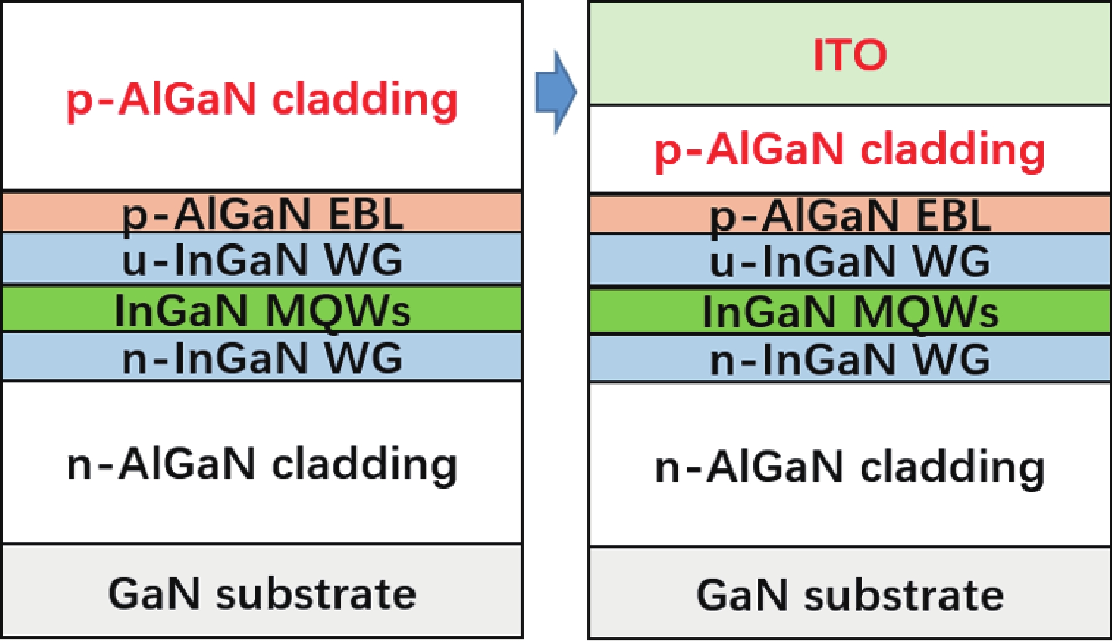
Fig. 1.
(Color online) The schematic layer structure of conventional and hybrid GaN-based LDs.
SHORT COMMUNICATIONS
Lei Hu1, Siyi Huang1, Zhi Liu1, Tengfeng Duan1, Si Wu1, Dan Wang1, Hui Yang2, Jun Wang3 and Jianping Liu1, 2,
Corresponding author: Jianping Liu, jp.liu@ganbright.com
| [1] |
Akasaki I, Amano H, Sota S, et al. Stimulated emission by current injection from an AlGaN/GaN/GaInN quantum well device. Jpn J Appl Phys, 1995, 34, L1517 doi: 10.7567/JJAP.34.L1517
|
| [2] |
Nakamura S, Senoh M, Nagahama S I, et al. InGaN-based multi-quantum-well-structure laser diodes. Jpn J Appl Phys, 1996, 35, L74 doi: 10.1143/JJAP.35.L74
|
| [3] |
Amano H, Kito M, Hiramatsu K, et al. P-type conduction in Mg-doped GaN treated with low-energy electron beam irradiation (LEEBI). Jpn J Appl Phys, 1989, 28, L2112 doi: 10.1143/JJAP.28.L2112
|
| [4] |
Nakamura S, Iwasa N, Senoh M, et al. Hole compensation mechanism of P-type GaN films. Jpn J Appl Phys, 1992, 31, 1258 doi: 10.1143/JJAP.31.1258
|
| [5] |
Nakamura S, Mukai T, Senoh M, et al. Thermal annealing effects on P-type Mg-doped GaN films. Jpn J Appl Phys, 1992, 31, L139 doi: 10.1143/JJAP.31.L139
|
| [6] |
Nakamura S. GaN growth using GaN buffer layer. Jpn J Appl Phys, 1991, 30, L1705 doi: 10.1143/JJAP.30.L1705
|
| [7] |
Nakamura S, Senoh M, Mukai T. High-power InGaN/GaN double-heterostructure violet light emitting diodes. Appl Phys Lett, 1993, 62, 2390 doi: 10.1063/1.109374
|
| [8] |
Nakamura S, Mukai T, Senoh M. Candela-class high-brightness InGaN/AlGaN double-heterostructure blue-light-emitting diodes. Appl Phys Lett, 1994, 64, 1687 doi: 10.1063/1.111832
|
| [9] |
Nakatsu Y, Nagao Y, Kozuru K, et al. High-efficiency blue and green laser diodes for laser displays. Gallium Nitride Materials and Devices XIV, 2019, 10918 doi: 10.1117/12.2505309
|
| [10] |
König H, Ali M, Bergbauer W, et al. Visible GaN laser diodes: from lowest thresholds to highest power levels. Novel In-Plane Semiconductor Lasers XVIII, 2019, 10939 doi: 10.1117/12.2511976
|
| [11] |
Liang F, Zhao D G, Liu Z S, et al. GaN-based blue laser diode with 6.0 W of output power under continuous-wave operation at room temperature. J Semicond, 2021, 42, 112801 doi: 10.1088/1674-4926/42/11/112801
|
| [12] |
Hu L, Li D Y, Liu J P, et al. High-power GaN-based blue laser diodes with 7.5 W of light output power under continuous-wave operation. Acta Photonica Sinic, 2022, 51(2), 0251209 doi: 10.3788/gzxb20225102.0251209
|
| [13] |
Li S Q, Guo Q Q, Deng H Q, et al. Gallium nitride blue laser diodes with pulsed current operation exceeding 15 W in optical output power. J Semicond, 2024, 45, 110501 doi: 10.1088/1674-4926/24080031
|
| [14] |
Kishimoto K, Hirao T, Morizumi T, et al. Development of highly efficient blue and green edge-emitting laser diodes. Gallium Nitride Materials and Devices XIX, 2024, 12886 doi: 10.1117/12.2692586
|
| [15] |
Liu J P, Zhang L Q, Li D Y, et al. GaN-based blue laser diodes with 2.2 W of light output power under continuous-wave operation. IEEE Photonics Technol Lett, 2017, 29, 2203 doi: 10.1109/LPT.2017.2770169
|
| [16] |
Liu J P, Li Z C, Zhang L Q, et al. Realization of InGaN laser diodes above 500 nm by growth optimization of the InGaN/GaN active region. Appl Phys Express, 2014, 7, 111001 doi: 10.7567/APEX.7.111001
|
| [17] |
Tian A Q, Liu J P, Zhang L Q, et al. Green laser diodes with low threshold current density via interface engineering of InGaN/GaN quantum well active region. Opt Express, 2017, 25, 415 doi: 10.1364/OE.25.000415
|
| [18] |
Hu L, Ren X Y, Liu J P, et al. High-power hybrid GaN-based green laser diodes with ITO cladding layer. Photon Res, 2020, 8, 279 doi: 10.1364/PRJ.381262
|
| [19] |
Mehari S, Cohen D A, Becerrea D L, et al. Optical gain and loss measurements of semipolar III-nitride laser diodes with ITO/thin-p-GaN cladding layers. 2018 76th Device Research Conference (DRC), 2018, 1 doi: 10.1109/DRC.2018.8442174
|
| [20] |
Chilwell J, Hodgkinson I. Thin-films field-transfer matrix theory of planar multilayer waveguides and reflection from prism-loaded waveguides. J Opt Soc Am A, 1984, 1, 742 doi: 10.1364/JOSAA.1.000742
|
| [21] |
Tian A Q, Hu L, Zhang L Q, et al. Design and growth of GaN-based blue and green laser diodes. Sci China Mater, 2020, 63, 1348 doi: 10.1007/s40843-020-1275-4
|
| [22] |
Tian A Q, Hu L, Li X, et al. Greatly suppressed potential inhomogeneity and performance improvement of c-plane InGaN green laser diodes. Sci China Mater, 2022, 65, 543 doi: 10.1007/s40843-021-1804-x
|
| [23] |
Tian A Q, Liu J P, Zhang L Q, et al. Green laser diodes with low operation voltage obtained by suppressing carbon impurity in AlGaN: Mg cladding layer. Phys Status Solidi C, 2016, 13, 245 doi: 10.1002/pssc.201510186
|
| [24] |
Jiang L R, Liu J P, Tian A Q, et al. GaN-based green laser diodes. J Semicond, 2016, 37, 111001 doi: 10.1088/1674-4926/37/11/111001
|


Article views: 2245 Times PDF downloads: 351 Times Cited by: 0 Times
Received: 02 December 2024 Revised: 16 December 2024 Online: Accepted Manuscript: 26 December 2024Uncorrected proof: 05 February 2025Published: 10 April 2025
| Citation: |
Lei Hu, Siyi Huang, Zhi Liu, Tengfeng Duan, Si Wu, Dan Wang, Hui Yang, Jun Wang, Jianping Liu. GaN-based blue laser diodes with output power of 5 W and lifetime over 20 000 h aged at 60 °C[J]. Journal of Semiconductors, 2025, 46(4): 040501. doi: 10.1088/1674-4926/24110039
****
L Hu, S Y Huang, Z Liu, T F Duan, S Wu, D Wang, H Yang, J Wang, and J P Liu, GaN-based blue laser diodes with output power of 5 W and lifetime over 20 000 h aged at 60 °C[J]. J. Semicond., 2025, 46(4), 040501 doi: 10.1088/1674-4926/24110039

|
 Lei Hu is the chip R & D manager of Suzhou Ganbright Optoelectronics Technology Co., Ltd. He earned his doctoral degree from School of Nano-Tech and Nano-Bionics, University of Science and Technology of China. His research focuses on fabrication and characterization of GaN-based blue and green laser diodes
 Jianping Liu is the founder of Suzhou Ganbright Optoelectronics Technology Co., Ltd, and a professor in Suzhou Institute of Nano-Tech and Nano-Bionics, Chinese Academy of Sciences. He earned his doctoral degree from Institute of Semiconductors, Chinese Academy of Sciences in 2004. He worked at Lab of Optoelectronics Technology at Beijing University of Technology from 2004 to 2006. He did postdoctoral research in Department of Electrical Engineering at Georgia Institute of Technology from 2006 to 2010. His research interests include MOCVD growth, GaN-based materials and devices
| [1] |
Akasaki I, Amano H, Sota S, et al. Stimulated emission by current injection from an AlGaN/GaN/GaInN quantum well device. Jpn J Appl Phys, 1995, 34, L1517 doi: 10.7567/JJAP.34.L1517
|
| [2] |
Nakamura S, Senoh M, Nagahama S I, et al. InGaN-based multi-quantum-well-structure laser diodes. Jpn J Appl Phys, 1996, 35, L74 doi: 10.1143/JJAP.35.L74
|
| [3] |
Amano H, Kito M, Hiramatsu K, et al. P-type conduction in Mg-doped GaN treated with low-energy electron beam irradiation (LEEBI). Jpn J Appl Phys, 1989, 28, L2112 doi: 10.1143/JJAP.28.L2112
|
| [4] |
Nakamura S, Iwasa N, Senoh M, et al. Hole compensation mechanism of P-type GaN films. Jpn J Appl Phys, 1992, 31, 1258 doi: 10.1143/JJAP.31.1258
|
| [5] |
Nakamura S, Mukai T, Senoh M, et al. Thermal annealing effects on P-type Mg-doped GaN films. Jpn J Appl Phys, 1992, 31, L139 doi: 10.1143/JJAP.31.L139
|
| [6] |
Nakamura S. GaN growth using GaN buffer layer. Jpn J Appl Phys, 1991, 30, L1705 doi: 10.1143/JJAP.30.L1705
|
| [7] |
Nakamura S, Senoh M, Mukai T. High-power InGaN/GaN double-heterostructure violet light emitting diodes. Appl Phys Lett, 1993, 62, 2390 doi: 10.1063/1.109374
|
| [8] |
Nakamura S, Mukai T, Senoh M. Candela-class high-brightness InGaN/AlGaN double-heterostructure blue-light-emitting diodes. Appl Phys Lett, 1994, 64, 1687 doi: 10.1063/1.111832
|
| [9] |
Nakatsu Y, Nagao Y, Kozuru K, et al. High-efficiency blue and green laser diodes for laser displays. Gallium Nitride Materials and Devices XIV, 2019, 10918 doi: 10.1117/12.2505309
|
| [10] |
König H, Ali M, Bergbauer W, et al. Visible GaN laser diodes: from lowest thresholds to highest power levels. Novel In-Plane Semiconductor Lasers XVIII, 2019, 10939 doi: 10.1117/12.2511976
|
| [11] |
Liang F, Zhao D G, Liu Z S, et al. GaN-based blue laser diode with 6.0 W of output power under continuous-wave operation at room temperature. J Semicond, 2021, 42, 112801 doi: 10.1088/1674-4926/42/11/112801
|
| [12] |
Hu L, Li D Y, Liu J P, et al. High-power GaN-based blue laser diodes with 7.5 W of light output power under continuous-wave operation. Acta Photonica Sinic, 2022, 51(2), 0251209 doi: 10.3788/gzxb20225102.0251209
|
| [13] |
Li S Q, Guo Q Q, Deng H Q, et al. Gallium nitride blue laser diodes with pulsed current operation exceeding 15 W in optical output power. J Semicond, 2024, 45, 110501 doi: 10.1088/1674-4926/24080031
|
| [14] |
Kishimoto K, Hirao T, Morizumi T, et al. Development of highly efficient blue and green edge-emitting laser diodes. Gallium Nitride Materials and Devices XIX, 2024, 12886 doi: 10.1117/12.2692586
|
| [15] |
Liu J P, Zhang L Q, Li D Y, et al. GaN-based blue laser diodes with 2.2 W of light output power under continuous-wave operation. IEEE Photonics Technol Lett, 2017, 29, 2203 doi: 10.1109/LPT.2017.2770169
|
| [16] |
Liu J P, Li Z C, Zhang L Q, et al. Realization of InGaN laser diodes above 500 nm by growth optimization of the InGaN/GaN active region. Appl Phys Express, 2014, 7, 111001 doi: 10.7567/APEX.7.111001
|
| [17] |
Tian A Q, Liu J P, Zhang L Q, et al. Green laser diodes with low threshold current density via interface engineering of InGaN/GaN quantum well active region. Opt Express, 2017, 25, 415 doi: 10.1364/OE.25.000415
|
| [18] |
Hu L, Ren X Y, Liu J P, et al. High-power hybrid GaN-based green laser diodes with ITO cladding layer. Photon Res, 2020, 8, 279 doi: 10.1364/PRJ.381262
|
| [19] |
Mehari S, Cohen D A, Becerrea D L, et al. Optical gain and loss measurements of semipolar III-nitride laser diodes with ITO/thin-p-GaN cladding layers. 2018 76th Device Research Conference (DRC), 2018, 1 doi: 10.1109/DRC.2018.8442174
|
| [20] |
Chilwell J, Hodgkinson I. Thin-films field-transfer matrix theory of planar multilayer waveguides and reflection from prism-loaded waveguides. J Opt Soc Am A, 1984, 1, 742 doi: 10.1364/JOSAA.1.000742
|
| [21] |
Tian A Q, Hu L, Zhang L Q, et al. Design and growth of GaN-based blue and green laser diodes. Sci China Mater, 2020, 63, 1348 doi: 10.1007/s40843-020-1275-4
|
| [22] |
Tian A Q, Hu L, Li X, et al. Greatly suppressed potential inhomogeneity and performance improvement of c-plane InGaN green laser diodes. Sci China Mater, 2022, 65, 543 doi: 10.1007/s40843-021-1804-x
|
| [23] |
Tian A Q, Liu J P, Zhang L Q, et al. Green laser diodes with low operation voltage obtained by suppressing carbon impurity in AlGaN: Mg cladding layer. Phys Status Solidi C, 2016, 13, 245 doi: 10.1002/pssc.201510186
|
| [24] |
Jiang L R, Liu J P, Tian A Q, et al. GaN-based green laser diodes. J Semicond, 2016, 37, 111001 doi: 10.1088/1674-4926/37/11/111001
|

 WeChat ID
Journal of Semiconductors © 2017 All Rights Reserved 京ICP备05085259号-2

 DownLoad:

