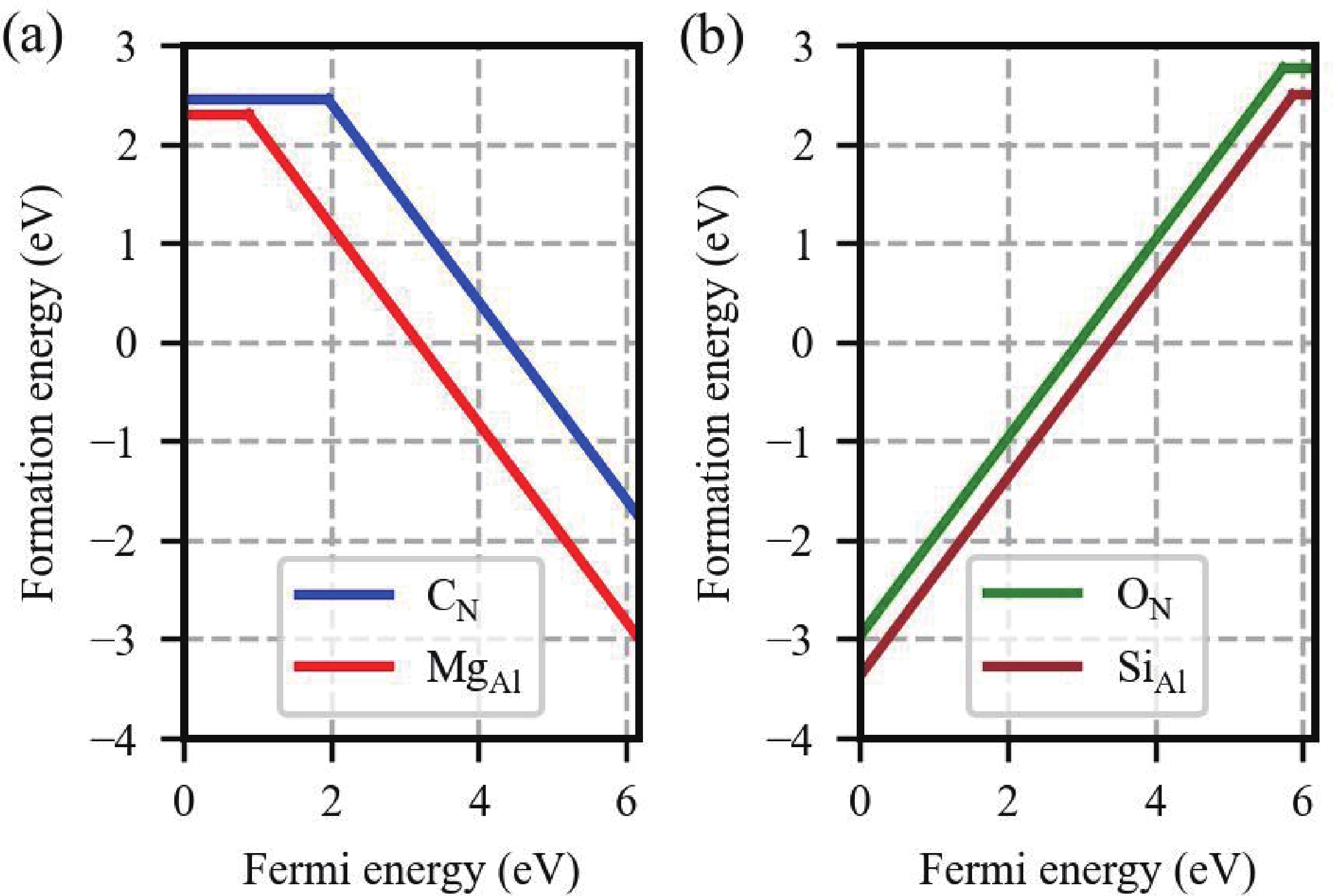
| [1] |
|
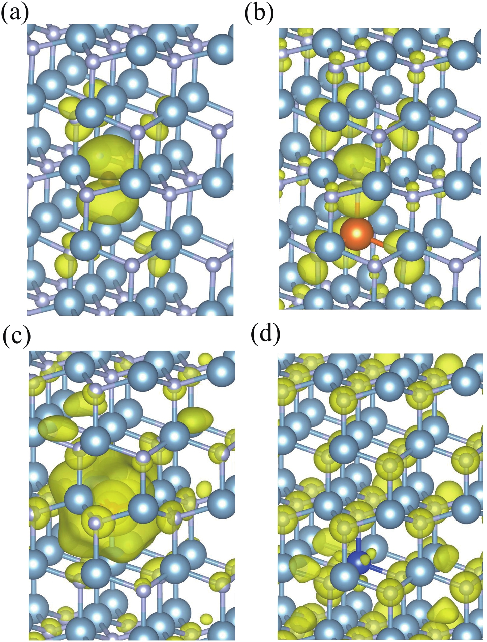
| [2] |
Yang J H, Yin W J, Park J S, et al. Enhanced p-type dopability of P and As in CdTe using non-equilibrium thermal processing. J Appl Phys, 2015, 118, 025102 doi: 10.1063/1.4926748 |
| [3] |
Li C, Li J B, Li S S, et al. Selection rule of preferred doping site for n-type oxides. Appl Phys Lett, 2012, 100, 262109 doi: 10.1063/1.4731766 |
| [4] |
Feneberg M, Leute R A R, Neuschl B, et al. High-excitation and high-resolution photoluminescence spectra of bulk AlN. Phys Rev B, 2010, 82, 075208 doi: 10.1103/PhysRevB.82.075208 |
| [5] |
Taniyasu Y, Kasu M, Makimoto T. An aluminium nitride light-emitting diode with a wavelength of 210 nanometres. Nature, 2006, 441, 325 doi: 10.1038/nature04760 |
| [6] |
Ahmad H, Engel Z, Matthews C M, et al. Realization of homojunction PN AlN diodes. J Appl Phys, 2022, 131, 175701 doi: 10.1063/5.0086314 |
| [7] |
Zheng W, Huang F, Zheng R S, et al. Photodetectors: Low-dimensional structure vacuum-ultraviolet-sensitive ( λ < 200 nm) photodetector with fast-response speed based on high-quality AlN micro/nanowire. Adv Mater, 2015, 27, 3971 doi: 10.1002/adma.201570176 |
| [8] |
Tsao J Y, Chowdhury S, Hollis M A, et al. Ultrawide-bandgap semiconductors: Research opportunities and challenges. Adv Electron Mater, 2018, 4, 1600501 doi: 10.1002/aelm.201600501 |
| [9] |
Nam K B, Nakarmi M L, Li J, et al. Mg acceptor level in AlN probed by deep ultraviolet photoluminescence. Appl Phys Lett, 2003, 83, 878 doi: 10.1063/1.1594833 |
| [10] |
Tang Y B, Bo X H, Xu J, et al. Tunable p-type conductivity and transport properties of AlN nanowires via Mg doping. ACS Nano, 2011, 5, 3591 doi: 10.1021/nn200963k |
| [11] |
Ahmad H, Lindemuth J, Engel Z, et al. Substantial P-type conductivity of AlN achieved via beryllium doping. Adv Mater, 2021, 33, 2104497 doi: 10.1002/adma.202104497 |
| [12] |
Taniyasu Y, Kasu M, Makimoto T. Electrical conduction properties of n-type Si-doped AlN with high electron mobility (>100 cm 2V –1s –1). Appl Phys Lett, 2004, 85, 4672 doi: 10.1063/1.1824181 |
| [13] |
Zhang Y, Liu W, Niu H B. Native defect properties and p-type doping efficiency in group-IIA doped wurtzite AlN. Phys Rev B, 2008, 77, 035201 doi: 10.1103/PhysRevB.77.035201 |
| [14] |
Gordon L, Lyons J L, Janotti A, et al. Hybrid functional calculations of DX centers in AlN and GaN. Phys Rev B, 2014, 89, 085204 doi: 10.1103/PhysRevB.89.085204 |
| [15] |
Wu R Q, Shen L, Yang M, et al. Enhancing hole concentration in AlN by Mg: O codoping: Ab initio study. Phys Rev B, 2008, 77, 073203 doi: 10.1103/PhysRevB.77.073203 |
| [16] |
Saks N S, Agarwal A K, Ryu S H, et al. Low-dose aluminum and boron implants in 4H and 6H silicon carbide. J Appl Phys, 2001, 90, 2796 doi: 10.1063/1.1392958 |
| [17] |
Capano M A, Santhakumar R, Venugopal R, et al. Phosphorus implantation into 4H-silicon carbide. J Electron Mater, 2000, 29, 210 doi: 10.1007/s11664-000-0144-y |
| [18] |
Iwami M. Silicon carbide: Fundamentals. Nucl Instrum Meth Phys Res Sect A Accel Spectrometers Detect Assoc Equip, 2001, 466, 406 doi: 10.1016/S0168-9002(01)00601-5 |
| [19] |
Kresse G, Furthmüller J. Efficient iterative schemes for ab-initio total-energy calculations using a plane-wave basis set. Phys Rev B, 1996, 54, 11169 doi: 10.1103/PhysRevB.54.11169 |
| [20] |
Kresse G, Furthmüller J. Efficiency of ab-initio total energy calculations for metals and semiconductors using a plane-wave basis set. Comput Mater Sci, 1996, 6, 15 doi: 10.1016/0927-0256(96)00008-0 |
| [21] |
|
| [22] |
Krukau A V, Vydrov O A, Izmaylov A F, et al. Influence of the exchange screening parameter on the performance of screened hybrid functionals. J Chem Phys, 2006, 125, 224106 doi: 10.1063/1.2404663 |
| [23] |
Cai X F, Yang J X, Zhang P, et al. Origin of deep be acceptor levels in nitride semiconductors: The roles of chemical and strain effects. Phys Rev Applied, 2019, 11, 034019 doi: 10.1103/PhysRevApplied.11.034019 |
| [24] |
Zhang X, Kang J, Wei S H. Defect modeling and control in structurally and compositionally complex materials. Nat Comput Sci, 2023, 3, 210 doi: 10.1038/s43588-023-00403-8 |
| [25] |
Freysoldt C, Neugebauer J, Van de Walle C G. Fully ab-initio finite-size corrections for charged-defect supercell calculations. Phys Rev Lett, 2009, 102, 016402 doi: 10.1103/PhysRevLett.102.016402 |
| [26] |
Freysoldt C, Neugebauer J, Van de Walle C G. Electrostatic interactions between charged defects in supercells. Phys Status Solidi B, 2011, 248, 1067 doi: 10.1002/pssb.201046289 |
| [27] |
Freysoldt C, Grabowski B, Hickel T, et al. First-principles calculations for point defects in solids. Rev Mod Phys, 2014, 86, 253 doi: 10.1103/RevModPhys.86.253 |
| [28] |
|
| [29] |
Ishii R, Yoshikawa A, Funato M, et al. Revisiting the substitutional Mg acceptor binding energy of AlN. Phys Rev B, 2023, 108, 035205 doi: 10.1103/PhysRevB.108.035205 |
| [30] |
Nakarmi M L, Nepal N, Ugolini C, et al. Correlation between optical and electrical properties of Mg-doped AlN epilayers. Appl Phys Lett, 2006, 89, 152120 doi: 10.1063/1.2362582 |


 Yi-Feng Zheng is currently an associate researcher at Wenzhou Institute, University of Chinese Academy of Sciences. He obtained his bachelor’s degree from Fudan University in 2014 and his doctor’s degree in physics from Fudan University in 2019. From 2019 to 2022, he worked as a post-doctor at Beijing Computational Science Research Center. His research focuses on the computational study of defects and semiconductor alloys.
 Su-Huai Wei is currently a professor and Dean of School of Physics at Eastern Institute of Technology. He obtained a Ph.D. in physics from the College of William and Mary in the United States in 1985. From 1985 to 2015, he worked at the National Renewable Energy Laboratory (NREL) and from 2015 to 2024, he served as Head of the Materials and Energy Division at the Beijing Computational Science Research Center. His research is focused on developing electronic band structure theory and computational methods. He is a Fellow of both the American Physical Society, and the Materials Research Society.
 DownLoad: