| [1] |
Ocio M, Albany H. Two valence band evidence and thermal energy gap in Pb 1−xSn xTe. Phys Lett A, 1968, 27(2), 72 doi: 10.1016/0375-9601(68)91125-0 |
| [2] |
Preier H. Recent advances in lead-chalcogenide diode lasers. Appl Phys, 1979, 20(3), 189 doi: 10.1007/BF00886018 |
| [3] |
Arachchige I, Kanatzidis M. Anomalous band gap evolution from band inversion in Pb 1−xSn xTe nanocrystals. Nano Lett, 2009, 9(4), 1583 doi: 10.1021/nl8037757 |
| [4] |
|
| [5] |
Dziawa P, Kowalski B J, Dybko K, et al. Topological crystalline insulator states in Pb 1−xSn xSe. Nat Mater, 2012, 11(12), 1023 doi: 10.1038/nmat3449 |
| [6] |
Xu S, Liu C, Alidoust N, et al. Observation of a topological crystalline insulator phase and topological phase transition in Pb 1−xSn xTe. Nat Commun, 2012, 3(1), 1192 doi: 10.1038/ncomms2191 |
| [7] |
Tanaka Y, Ren Z, Sato T, et al. Experimental realization of a topological crystalline insulator in SnTe. Nat Phys, 2012, 8(11), 800 doi: 10.1038/nphys2442 |
| [8] |
Polley C M, Dziawa P, Reszka A, et al. Observation of topological crystalline insulator surface states on (111)-oriented Pb 1−xSn xSe films. Phys Rev B, 2014, 89(7), 075317 doi: 10.1103/PhysRevB.89.075317 |
| [9] |
Dimmock J, Melngailis I, Strauss A. Band structure and laser action in Pb xSn 1−xTe. Phys Rev Lett, 1966, 16(26), 1193 doi: 10.1103/PhysRevLett.16.1193 |
| [10] |
Kahn A. Fermi level, work function and vacuum level. Mater Horiz, 2016, 3(1), 7 doi: 10.1039/C5MH00160A |
| [11] |
Desjonqures M, Spanjaard D. Concepts in surface physics. Berlin: Springer, 1996
|
| [12] |
Woodruff D. Modern techniques of surface science. Cambridge: Cambridge University Press, 2016
|
| [13] |
Janssen A P, Akhter P, Harland C J, et al. High spatial resolution surface potential measurements using secondary electrons. Surf Sci, 1980, 93(2), 453
|
| [14] |
Gnaser H. Initial stages of cesium incorporation on keV-Cs +-irradiated surfaces: Positive-ion emission and work-function changes. Phys Rev B, 1996, 54(23), 17141 doi: 10.1103/PhysRevB.54.17141 |
| [15] |
Gnaser H. Exponential scaling of sputtered negative-ion yields with transient work-function changes on Cs + bombarded surfaces. Phys Rev B, 1996, 54(23), 16456 doi: 10.1103/PhysRevB.54.16456 |
| [16] |
Yamazaki H, Nakamura S. Work-function changes in high-dose B-implanted Si with keV Cs + bombardment. Phys Rev B, 1999, 59(19), 12298 doi: 10.1103/PhysRevB.59.12298 |
| [17] |
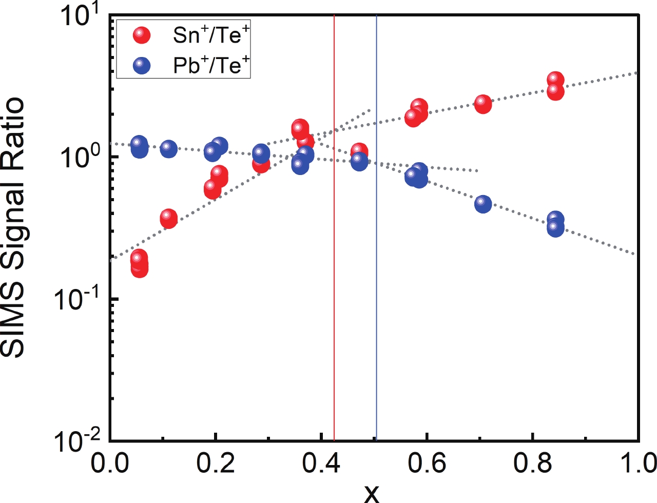
Khosravizadeh Z, Dziawa P, Dad S, et al. Secondary ion mass spectrometry characterization of matrix composition in topological crystalline insulator Pb 1−xSn xTe. Thin Solid Films, 2023, 781, 139974 doi: 10.1016/j.tsf.2023.139974 |
| [18] |
Berchenko N, Vitchev R, Trzyna M, et al. Surface oxidation of SnTe topological crystalline insulator. Appl Surf Sci, 2018, 452, 134 doi: 10.1016/j.apsusc.2018.04.246 |
| [19] |
Yu M. Sputtering by particle bombardment III. Berlin: Springer, 1991
|
| [20] |
Mönch W. Semiconductor surfaces and interfaces. Berlin: Springer, 1995
|
| [21] |
|
| [22] |
Blaise G, Slodzian G. Effets comparés de l’oxygène sur l’émission ionique et le potentiel de surface des métaux. Surf Sci, 1973, 40(3), 708 doi: 10.1016/0039-6028(73)90154-4 |
| [23] |
|
| [24] |
Nørskov J K, Lundqvist B I. Secondary-ion emission probability in sputtering. Phys Rev B, 1979, 19(11), 5661 doi: 10.1103/PhysRevB.19.5661 |
| [25] |
Buchauer L. Superconductivity and Fermi surface of Tl: PbTe. Master Dissertation, École supérieure de physique et de chimie industrielles de la ville de Paris/Technische Universität Darmstadt, 2017
|
| [26] |
He J, Androulakis J, Kanatzidis M, et al. Seeing is believing: Weak phonon scattering from nanostructures in alkali metal-doped lead telluride. Nano Lett, 2012, 12(1), 343 doi: 10.1021/nl203626n |
| [27] |
Kowalczyk L, Szczerbakow A. Temperature and composition dependence of the energy band gap of Pb xMn ySn xSe alloys. Acta Phys Pol A, 1985, 67(1), 189 doi: 10.1007/BF00618116 |
| [28] |
Łusakowski A, Bogusławski P, Story T. Band structure and topological phases of Pb 1−x−ySn xMn yTe by ab initio calculations. Phys Rev B, 2021, 103(4), 045202 doi: 10.1103/PhysRevB.103.045202 |


 Zeinab Khosravizadeh is a Ph.D. candidate in solid-state physics at the Polish Academy of Sciences. Her research focuses on material science and semiconductor physics, specializing in secondary ion mass spectrometry, advanced materials characterization. She has also studied diffusion of dopants in semiconductor materials, and synthesizing magnetic Nano particles.
 Rafał Jakiela Rafal Jakiela is currently a Professor of Physics and Head of the secondary ion mass spectrometry laboratory at the Polish Academy of Sciences. He received his PhD from the Polish Academy of Science in 2005. He is an expert in analysing solid-state materials using SIMS. His studies focus on the diffusion and segregation of dopants in semiconductor materials.
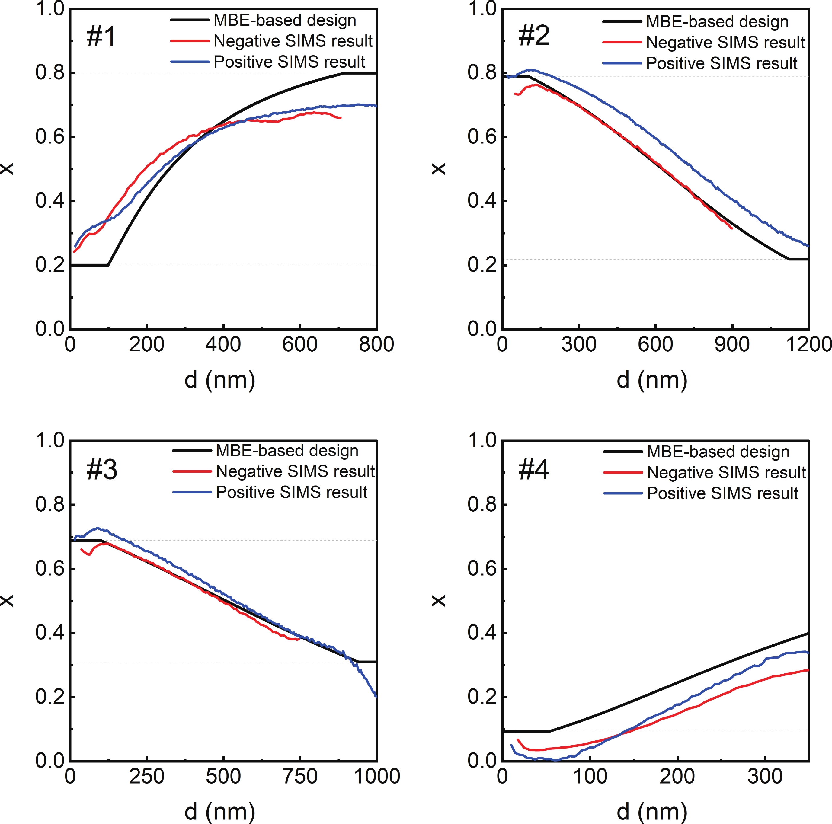
 DownLoad: