


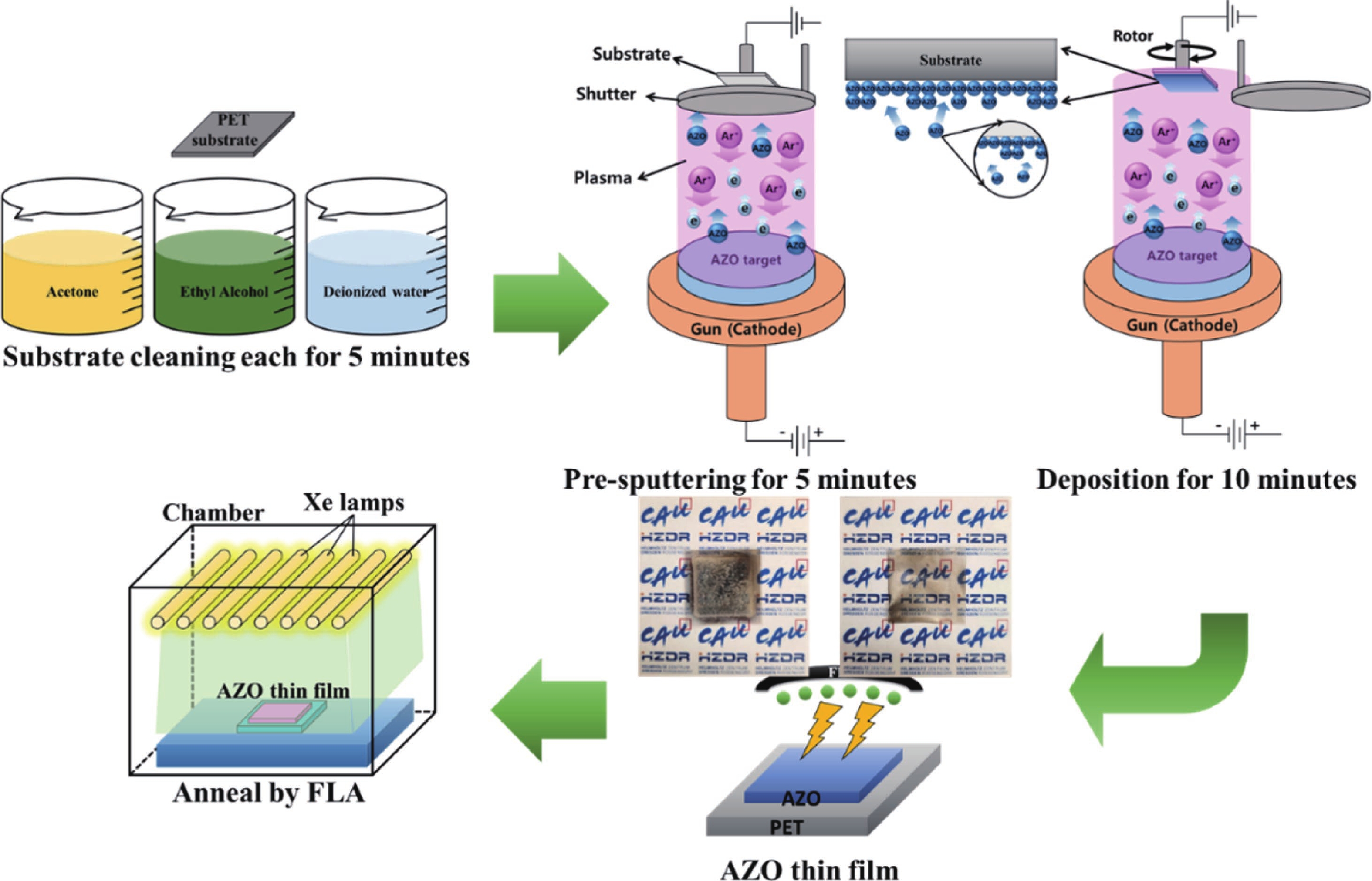
Fig. 1.
(Color online) Schematic diagram of the thin film growth and flash lamp annealing of the AZO on PET substrate.
ARTICLES
Juwon Lee1, Chang-Hyeon Jo1, Gwangseop Lee1, Min-Sung Bae1, Slawomir Prucnal3, Shengqiang Zhou3, Muhammad Zubair Khan4, Osama Gohar5, Mohsin Saleem6, and Jung-Hyuk Koh1, 2,
Corresponding author: Mohsin Saleem, mohsin852@cau.ac.kr; mohsin852604@gmail.com; Jung-Hyuk Koh, jhkoh@cau.ac.kr
Abstract: In this study, aluminum-doped zinc oxide (AZO) thin films were deposited onto a low-temperature polyethylene terephthalate (PET) substrate using DC magnetron sputtering. Deposition parameters included power range of 100−300 W, a working pressure of 15 mTorr, and a substrate temperature of 50 °C. Post-deposition, flash lamp annealing (FLA) was employed as a rapid thermal processing method with a pulse duration of 1.7 ms and energy density of 7 J·cm−2, aimed at enhancing the film's quality while preserving the temperature-sensitive PET substrate. FLA offers advantages over conventional annealing, including shorter processing times and improved material properties. The structural, optical, and electrical characteristics of the AZO films were assessed using X-ray diffraction, field emission scanning electron microscopy coupled with energy-dispersive X-ray spectroscopy, ultraviolet−visible spectroscopy, and Hall effect measurements. The results demonstrated that properties of AZO films varied with deposition and annealing conditions. Films deposited at 200 W and subjected to FLA exhibited superior crystallinity, with average visible light transmittance exceeding 80% and resistivity as low as 0.38 Ω·cm representing 95% improvement in transmittance. Electrical analysis revealed that carrier concentration, mobility, and resistivity were influenced by both sputtering and annealing parameters. These findings underscore the effectiveness of FLA in optimizing AZO thin film properties, highlighting potential in optoelectronics applications.
Keywords: flash lamp annealing, AZO, thin film, PET, sputtering
| [1] |
Kim H, Gilmore C M, Piqué A, et al. Electrical, optical, and structural properties of indium–tin–oxide thin films for organic light-emitting devices. J Appl Phys, 1999, 86, 6451 doi: 10.1063/1.371708
|
| [2] |
Ma Z Z, Li Z R, Liu K, et al. Indium-tin-oxide for high-performance electro-optic modulation. Nanophotonics, 2015, 4, 198 doi: 10.1515/nanoph-2015-0006
|
| [3] |
Bae M S, Lee J W, Koh J H. Synthesis and characterization of multi-phase structure, optical and electrical properties on (Ga–Sn) oxide composite thin film by sol-gel method. Mater Chem Phys, 2023, 293, 126960 doi: 10.1016/j.matchemphys.2022.126960
|
| [4] |
Kokubun Y, Miura K, Endo F, et al. Sol-gel prepared β-Ga2O3 thin films for ultraviolet photodetectors. Appl Phys Lett, 2007, 90, 031912 doi: 10.1063/1.2432946
|
| [5] |
Aktas S, Caglar M. Electrical performance and HfO2 gate dielectric optimization of SnO2 thin film phototransistors. Mater Sci Eng B, 2024, 308, 117587 doi: 10.1016/j.mseb.2024.117587
|
| [6] |
Feng X Q, Cheng R Q, Yin L, et al. Two-dimensional oxide crystals for device applications: Challenges and opportunities. Adv Mater, 2024, 36, 2304708 doi: 10.1002/adma.202304708
|
| [7] |
Shoeb M, Ahmad S, Mashkoor F, et al. Investigating the size-dependent structural, optical, dielectric, and photocatalytic properties of benign-synthesized ZnO nanoparticles. J Phys Chem Solids, 2024, 184, 111707 doi: 10.1016/j.jpcs.2023.111707
|
| [8] |
Korhonen E, Tuomisto F, Gogova D, et al. Electrical compensation by Ga vacancies in Ga2O3 thin films. Appl Phys Lett, 2015, 106, 242103 doi: 10.1063/1.4922814
|
| [9] |
Teherani F H, Khodaparast G A, Xu Y V, et al. A review of the growth, doping, and applications of Beta-Ga2O3 thin films. Oxide-based Materials and Devices IX, 2018, 105330R doi: 10.1117/12.2302471
|
| [10] |
Li C T, Qiu T F, Li C, et al. Highly flexible and acid–alkali resistant TiN nanomesh transparent electrodes for next-generation optoelectronic devices. ACS Nano, 2023, 17, 24763 doi: 10.1021/acsnano.3c05211
|
| [11] |
Kim J M, Thiyagarajan P, Rhee S W. Deposition of Al-doped ZnO films on polyethylene naphthalate substrate with radio frequency magnetron sputtering. Thin Solid Films, 2010, 518, 5860 doi: 10.1016/j.tsf.2010.05.098
|
| [12] |
Yang W J, Tsao C C, Hsu C Y, et al. Fabrication and characterization of transparent conductive ZnO: Al thin films deposited on polyethylene terephthalate substrates. J Am Ceram Soc, 2012, 95, 2140 doi: 10.1111/j.1551-2916.2012.05178.x
|
| [13] |
Kim Y H, Lee J W, Murakami R I. Dependences of sputtering times on the structural and electrical properties of ZnO/Ag/ZnO thin films on PET by DC sputtering. IEEE Trans Nanotechnol, 2013, 12, 991 doi: 10.1109/TNANO.2013.2274596
|
| [14] |
Mohammed D W, Ameen R M, Waddingham R, et al. Assessing the effect of twisting and twisting fatigue on ZnO: Al thin film performance on PEN and PET substrates. Micromachines, 2024, 15, 853 doi: 10.3390/mi15070853
|
| [15] |
Akhmedov A K, Murliev E K, Asvarov A S, et al. Transparent conductive indium zinc oxide films: Temperature and oxygen dependences of the electrical and optical properties. Coatings, 2022, 12, 1583 doi: 10.3390/coatings12101583
|
| [16] |
Singh M, Scotognella F. Recent progress in solution processed aluminum and co-doped ZnO for transparent conductive oxide applications. Micromachines, 2023, 14, 536 doi: 10.3390/mi14030536
|
| [17] |
Sygletou M, Bisio F, Benedetti S, et al. Transparent conductive oxide-based architectures for the electrical modulation of the optical response: A spectroscopic ellipsometry study. J Vac Sci Technol B, 2019, 37, 061209 doi: 10.1116/1.5122175
|
| [18] |
de Oliveira G H I, Escote M T, Nantes I L, et al. Versatile r. f. magnetron sputtering doping method to produce aluminum-doped zinc oxide films. J Am Ceram Soc, 2024, 107, 4729 doi: 10.1111/jace.19753
|
| [19] |
Zhu B L, Wang C C, Xie T, et al. Highly transparent conductive ZnO films prepared by reactive RF sputtering with Zn/ZnO composite target. Appl Phys A, 2021, 127, 668 doi: 10.1007/s00339-021-04826-w
|
| [20] |
Kaneko K, Uno K, Jinno R, et al. Prospects for phase engineering of semi-stable Ga2O3 semiconductor thin films using mist chemical vapor deposition. J Appl Phys, 2022, 131, 090902 doi: 10.1063/5.0069554
|
| [21] |
Rúa A, Díaz R D, Lysenko S, et al. Semiconductor-insulator transition in VO2 (B) thin films grown by pulsed laser deposition. J Appl Phys, 2015, 118, 125308 doi: 10.1063/1.4931887
|
| [22] |
Vorobyova M, Biffoli F, Giurlani W, et al. PVD for decorative applications: A review. Materials, 2023, 16, 4919 doi: 10.3390/ma16144919
|
| [23] |
Aggarwal R, Kaushik D K. Structural and optical studies on sol-gel driven spin-coated CdS thin films. J Phys: Conf Ser, 2022, 2267, 012012 doi: 10.1088/1742-6596/2267/1/012012
|
| [24] |
Ulbrandt J G, Zhang X Z, Headrick R L, et al. Fast nonthermal processes in pulsed laser deposition. Phys Rev B, 2020, 101, 241406 doi: 10.1103/PhysRevB.101.241406
|
| [25] |
Liu H Y, Wang X Q, Li M Y, et al. Optical and electrical properties of Al doped ZnO thin film with preferred orientation in situ grown at room temperature. Ceram Int, 2019, 45, 14347 doi: 10.1016/j.ceramint.2019.04.149
|
| [26] |
Oke J A, Jen T C. Atomic layer deposition and other thin film deposition techniques: From principles to film properties. J Mater Res Technol, 2022, 21, 2481 doi: 10.1016/j.jmrt.2022.10.064
|
| [27] |
Chang S H, Koo J H, Yoo J, et al. Flexible and stretchable light-emitting diodes and photodetectors for human-centric optoelectronics. Chem Rev, 2024, 124, 768 doi: 10.1021/acs.chemrev.3c00548
|
| [28] |
Timans P, Gelpey J, McCoy S, et al. Millisecond annealing: Past, present and future. MRS Online Proc Libr, 2006, 912, 101 doi: 10.1557/PROC-0912-C01-01
|
| [29] |
Zhu M H, Liu W W, Ke W J, et al. Millisecond-pulsed photonically-annealed tin oxide electron transport layers for efficient perovskite solar cells. J Mater Chem A, 2017, 5, 24110 doi: 10.1039/C7TA07969A
|
| [30] |
Serpelloni M, Cantù E, Borghetti M, et al. Printed smart devices on cellulose-based materials by means of aerosol-jet printing and photonic curing. Sensors, 2020, 20, 841 doi: 10.3390/s20030841
|
| [31] |
Chen X B, Sastre J, Rumpel M, et al. Photonic methods for rapid crystallization of LiMn2O4 cathodes for solid-state thin-film batteries. J Power Sources, 2021, 495, 229424 doi: 10.1016/j.jpowsour.2020.229424
|
| [32] |
Jang Y R, Joo S J, Chu J H, et al. A review on intense pulsed light sintering technologies for conductive electrodes in printed electronics. Int J Precis Eng Manuf Green Technol, 2021, 8, 327 doi: 10.1007/s40684-020-00193-8
|
| [33] |
Attallah A G, Prucnal S, Buttering M, et al. Millisecond flash lamp curing for porosity generation in thin films. Sci Rep, 2023, 13, 7765 doi: 10.1038/s41598-023-34748-x
|
| [34] |
Tanimura H, Ota Y, Kawarazaki H, et al. Fabrication of thin ferroelectric Hf0.5Zr0.5O2 films by millisecond flash lamp annealing. Jpn J Appl Phys, 2023, 62, SC1044 doi: 10.35848/1347-4065/acb1b7
|
| [35] |
Jo J W, Kim K T, Park H H, et al. High-speed and low-temperature atmospheric photo-annealing of large-area solution-processed IGZO thin-film transistors by using programmable pulsed operation of xenon flash lamp. J Korean Phys Soc, 2019, 74, 1052 doi: 10.3938/jkps.74.1052
|
| [36] |
Nuchuay P, Laongwan C, Promcham W, et al. A study of the electrical and optical properties of AZO thin film by controlling pulse frequency of HiPIMS. J Met Mater Miner, 2023, 33, 103 doi: 10.55713/jmmm.v33i2.1696
|
| [37] |
Rebohle L, Prucnal S, Reichel D. Flash lamp annealing. Switzerland: Springer Cham, 2019
|
| [38] |
Zhang G X, Steuer O, Li R, et al. Al-delta-doped ZnO films made by atomic layer deposition and flash-lamp annealing for low-emissivity coating. Appl Surf Sci, 2024, 648, 159046 doi: 10.1016/j.apsusc.2023.159046
|
| [39] |
Moonen P F, Yakimets I, Huskens J. Fabrication of transistors on flexible substrates: From mass-printing to high-resolution alternative lithography strategies. Adv Mater, 2012, 24, 5526 doi: 10.1002/adma.201202949
|
| [40] |
Bae M S, Kim S H, Baek J S, et al. Comparative study of high-temperature annealed and RTA process β-Ga2O3 thin film by sol–gel process. Coatings, 2021, 11, 1220 doi: 10.3390/coatings11101220
|
| [41] |
Jun M C, Koh J H. Effects of annealing temperature on properties of Al-doped ZnO thin films prepared by sol-gel dip-coating. J Electr Eng Technol, 2013, 8, 163 doi: 10.5370/JEET.2013.8.1.163
|
| [42] |
Kim J, Ji J H, Min S W, et al. Enhanced conductance properties of UV laser/RTA annealed Al-doped ZnO thin films. Ceram Int, 2017, 43, 3900 doi: 10.1016/j.ceramint.2016.12.063
|
| [43] |
Aoun Y, Benhaoua B, Benramache S, et al. Effect of annealing temperature on structural, optical and electrical properties of zinc oxide (ZnO) thin films deposited by spray pyrolysis technique. Optik, 2015, 126, 5407 doi: 10.1016/j.ijleo.2015.08.267
|
| [44] |
Challali F, Mendil D, Touam T, et al. Effect of RF sputtering power and vacuum annealing on the properties of AZO thin films prepared from ceramic target in confocal configuration. Mater Sci Semicond Process, 2020, 118, 105217 doi: 10.1016/j.mssp.2020.105217
|
| [45] |
Lee K E, Wang M S, Kim E J, et al. Structural, electrical and optical properties of sol–gel AZO thin films. Curr Appl Phys, 2009, 9, 683 doi: 10.1016/j.cap.2008.06.006
|
| [46] |
Haider J, Rahman M, Corcoran B, et al. Simulation of thermal stress in magnetron sputtered thin coating by finite element analysis. J Mater Process Technol, 2005, 168, 36 doi: 10.1016/j.jmatprotec.2004.09.093
|
| [47] |
Park S U, Koh J H. Low temperature rf-sputtered in and Al Co-doped ZnO thin films deposited on flexible PET substrate. Ceram Int, 2014, 40, 10021 doi: 10.1016/j.ceramint.2014.02.101
|
| [48] |
Phiri R R, Oladijo O P, Akinlabi E T. Defect formation and surface evolution of thin film materials. Proceedings of the International Conference on Industrial Engineering and Operations Management, 2018, 1087
|
| [49] |
Abadias G, Chason E, Keckes J, et al. Review Article: Stress in thin films and coatings: Current status, challenges, and prospects. J Vac Sci Technol A Vac Surf Films, 2018, 36, 020801 doi: 10.1116/1.5011790
|
| [50] |
Swinehart D F. The beer-lambert law. J Chem Educ, 1962, 39, 333 doi: 10.1021/ed039p333
|
| [51] |
Park H, Qamar Hussain S, Velumani S, et al. Influence of working pressure on the structural, optical and electrical properties of sputter deposited AZO thin films. Mater Sci Semicond Process, 2015, 37, 29 doi: 10.1016/j.mssp.2014.12.076
|
| [52] |
Zhang Z Y, Bao C G, Yao W J, et al. Influence of deposition temperature on the crystallinity of Al-doped ZnO thin films at glass substrates prepared by RF magnetron sputtering method. Superlattices Microstruct, 2011, 49, 644 doi: 10.1016/j.spmi.2011.04.002
|
| [53] |
Shi Q, Zhou K S, Dai M J, et al. Room temperature preparation of high performance AZO films by MF sputtering. Ceram Int, 2013, 39, 1135 doi: 10.1016/j.ceramint.2012.07.037
|
| [54] |
He B, Xu J, Xing H Z, et al. The effect of substrate temperature on high quality c-axis oriented AZO thin films prepared by DC reactive magnetron sputtering for photoelectric device applications. Superlattices Microstruct, 2013, 64, 319 doi: 10.1016/j.spmi.2013.10.003
|
| [55] |
Zhou X F, Sun Q W, Zhai D, et al. Excellent catalytic performance of molten-salt-synthesized Bi0.5Na0.5TiO3 nanorods by the piezo-phototronic coupling effect. Nano Energy, 2021, 84, 105936 doi: 10.1016/j.nanoen.2021.105936
|
| [56] |
Constantinescu C, Matei A, Ionita I, et al. Azo-derivatives thin films grown by matrix-assisted pulsed laser evaporation for non-linear optical applications. Appl Surf Sci, 2014, 302, 69 doi: 10.1016/j.apsusc.2013.12.068
|
| [57] |
Khatami S, Fekri Aval L, Behzadi Pour G. Investigation of nanostructure and optical properties of flexible AZO thin films at different powers of RF magnetron sputtering. Nano, 2018, 13, 1850062 doi: 10.1142/S1793292018500625
|
| [58] |
Poddar N P, Mukherjee S K. Effect of substrates and post-deposition annealing on rf-sputtered Al-doped ZnO (AZO) thin films. J Mater Sci Mater Electron, 2019, 30, 14269 doi: 10.1007/s10854-019-01796-x
|
| [59] |
Islam M M, Ishizuka S, Yamada A, et al. Thickness study of Al: ZnO film for application as a window layer in Cu(In1–xGax)Se2 thin film solar cell. Appl Surf Sci, 2011, 257, 4026 doi: 10.1016/j.apsusc.2010.11.169
|
| [60] |
Poruba A, Fejfar A, Remeš Z, et al. Optical absorption and light scattering in microcrystalline silicon thin films and solar cells. J Appl Phys, 2000, 88, 148 doi: 10.1063/1.373635
|
| [61] |
Kang J, Park D, Lee D H, et al. Enhanced electrical properties of AZO/IZO multilayered thin film with post laser annealing process. J Nanosci Nanotechnol, 2021, 21, 1971 doi: 10.1166/jnn.2021.18913
|
| [62] |
Prucnal S, Rebohle L, Skorupa W. Doping by flash lamp annealing. Mater Sci Semicond Process, 2017, 62, 115 doi: 10.1016/j.mssp.2016.10.040
|
| [63] |
Skorupa W, Schumann T, Rebohle L. Millisecond thermal processing using flash lamps for the advancement of thin layers and functional coatings. Surf Coat Technol, 2017, 314, 169 doi: 10.1016/j.surfcoat.2016.08.010
|
| [64] |
Gondoni P, Ghidelli M, Di Fonzo F, et al. Structure-dependent optical and electrical transport properties of nanostructured Al-doped ZnO. Nanotechnology, 2012, 23, 365706 doi: 10.1088/0957-4484/23/36/365706
|
| [65] |
Pei Z L, Zhang X B, Zhang G P, et al. Transparent conductive ZnO: Al thin films deposited on flexible substrates prepared by direct current magnetron sputtering. Thin Solid Films, 2006, 497, 20 doi: 10.1016/j.tsf.2005.09.110
|
| [66] |
Huang C S, Liu C C. The optical and electrical properties of gallium-doped ZnO thin film with post-annealing processes of various atmospheres. Microelectron Eng, 2015, 148, 59 doi: 10.1016/j.mee.2015.08.002
|
| [67] |
Lin C L, Wang F H, Jhuang H S, et al. Effects of different annealing temperatures on the physical, optical, and electrical characteristics and chemical bonds of Ga and F Co-doped ZnO films. J Mater Res Technol, 2020, 9, 6331 doi: 10.1016/j.jmrt.2020.03.046
|
| [68] |
Chen T H, Chen T Y. Effects of annealing temperature on properties of Ti-Ga–doped ZnO films deposited on flexible substrates. Nanomaterials, 2015, 5, 1831 doi: 10.3390/nano5041831
|
| [69] |
Lin Y C, Hsu C Y, Hung S K, et al. Influence of TiO2 buffer layer and post-annealing on the quality of Ti-doped ZnO thin films. Ceram Int, 2013, 39, 5795 doi: 10.1016/j.ceramint.2012.12.099
|
| [70] |
Hsueh K P, Cheng Y C, Lin W Y, et al. High-temperature stability of postgrowth-annealed Al-doped MgxZn1-xO films without the phase separation effect. J Vac Sci Technol B, 2012, 30, 061201 doi: 10.1116/1.4754813
|
| [71] |
Horng R H, Ou S L, Huang C Y, et al. Effects of Ga concentration and rapid thermal annealing on the structural, optoelectronic and photoluminescence properties of Ga-doped ZnO thin films. Thin Solid Films, 2016, 605, 30 doi: 10.1016/j.tsf.2015.12.006
|
| [72] |
Kim D K, Kim H B. Effect of post-annealing time on the properties of sputtered Al-doped ZnO thin films. J Mater Sci Mater Electron, 2016, 27, 11366 doi: 10.1007/s10854-016-5261-3
|
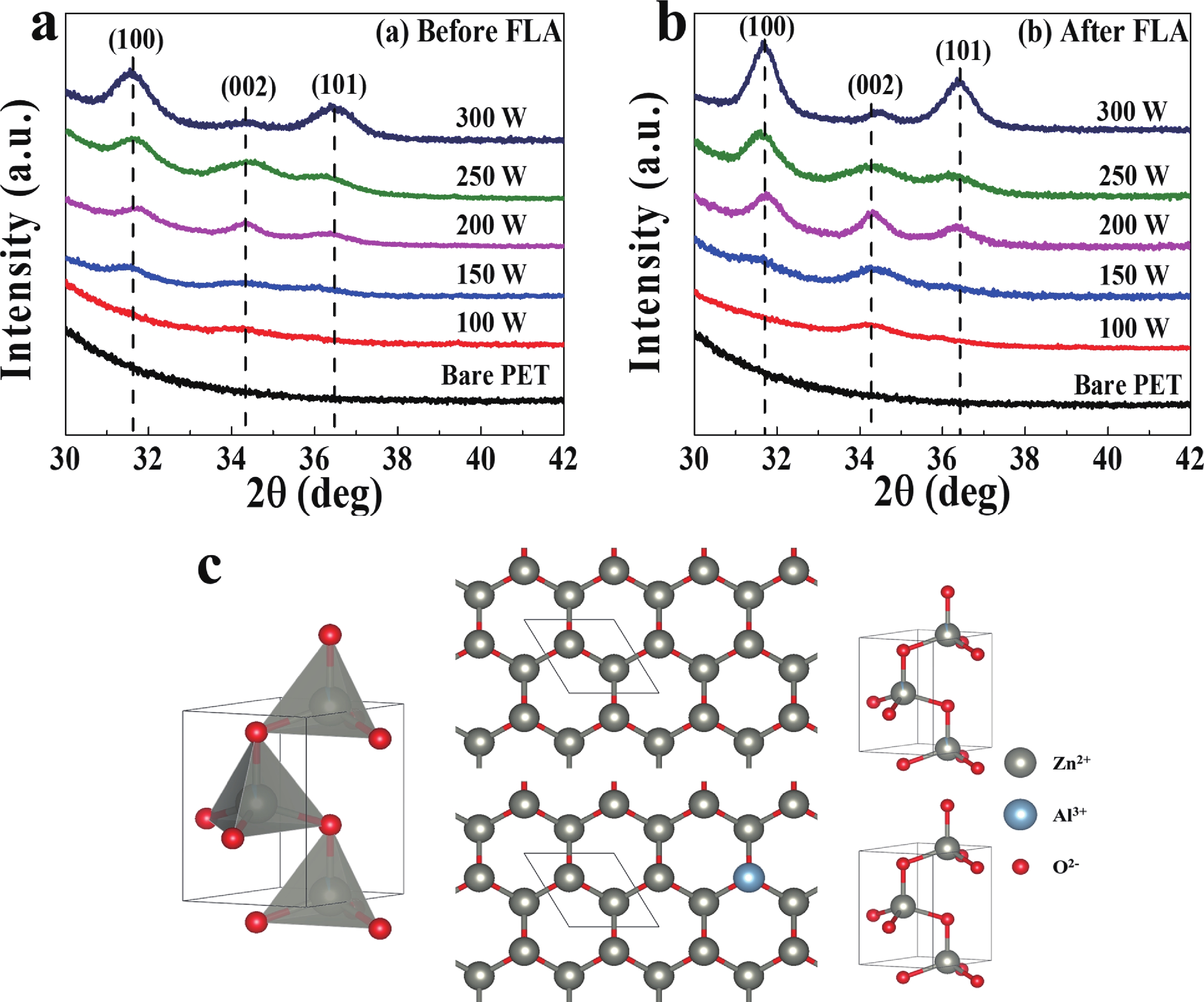
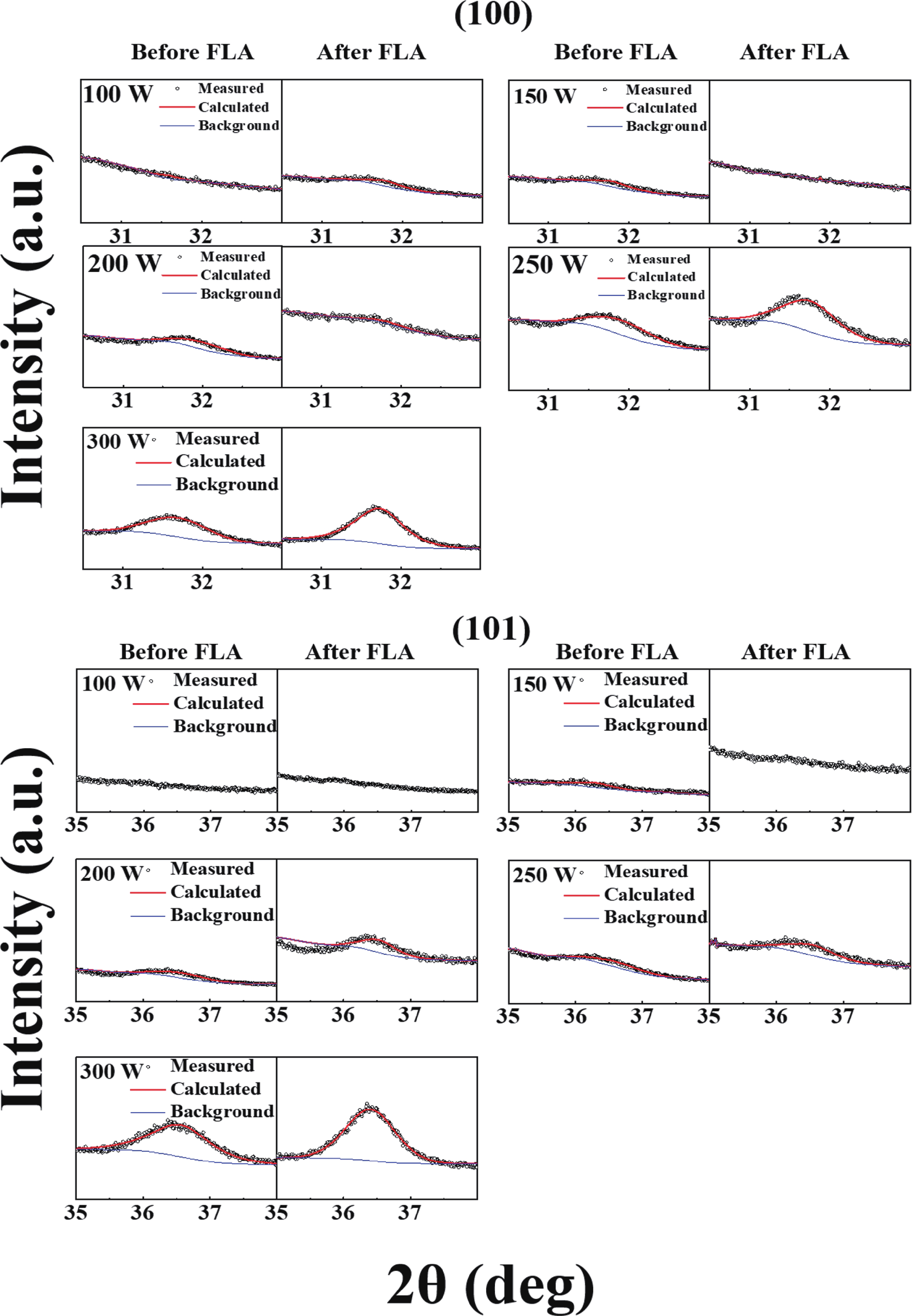
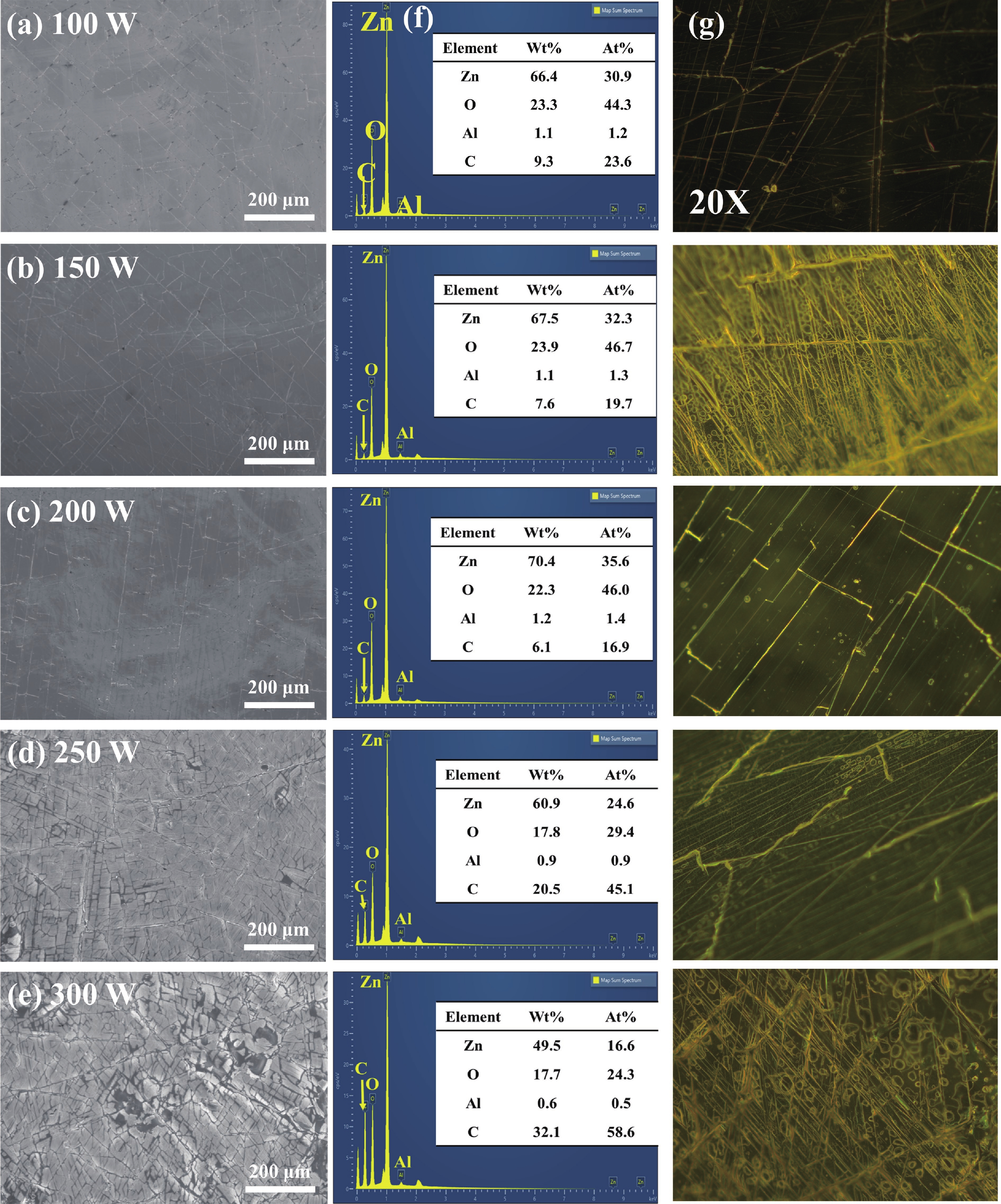

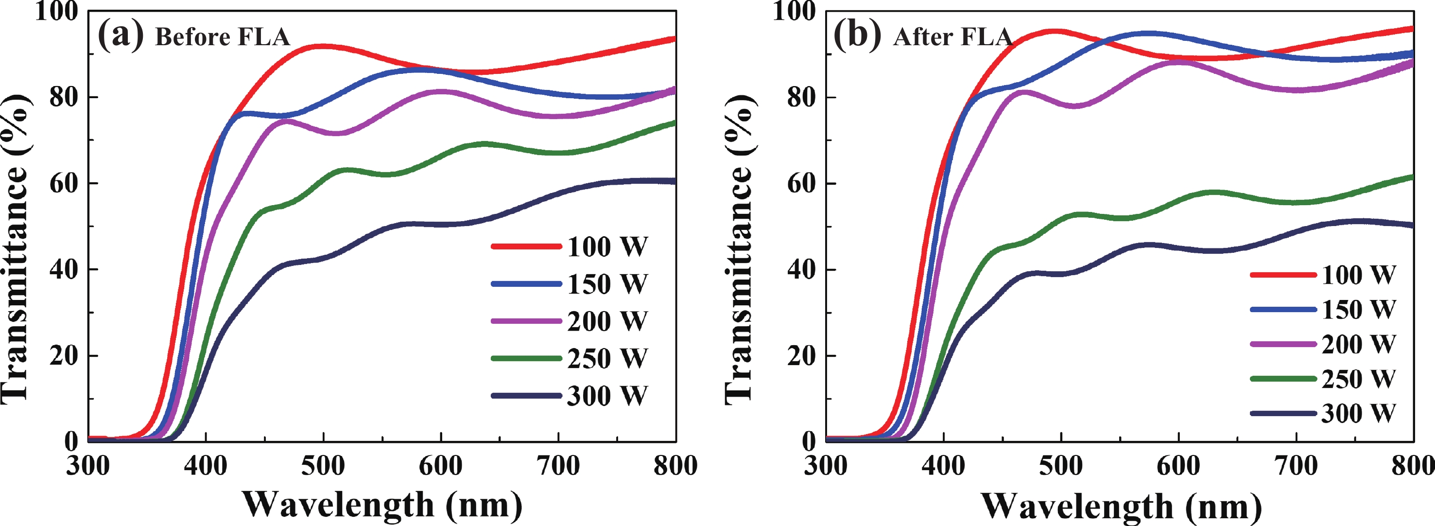

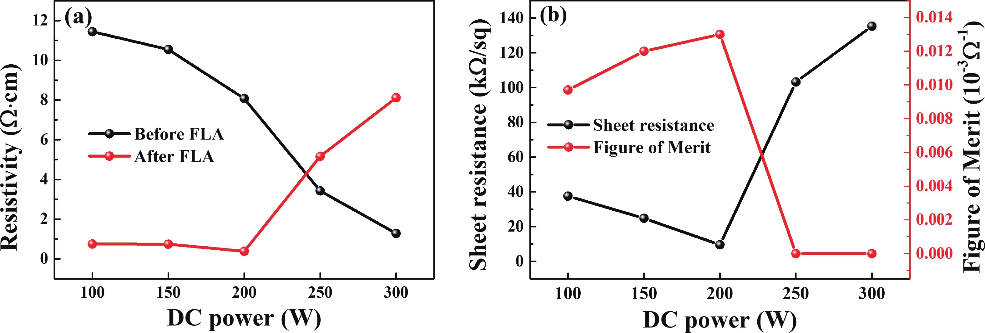
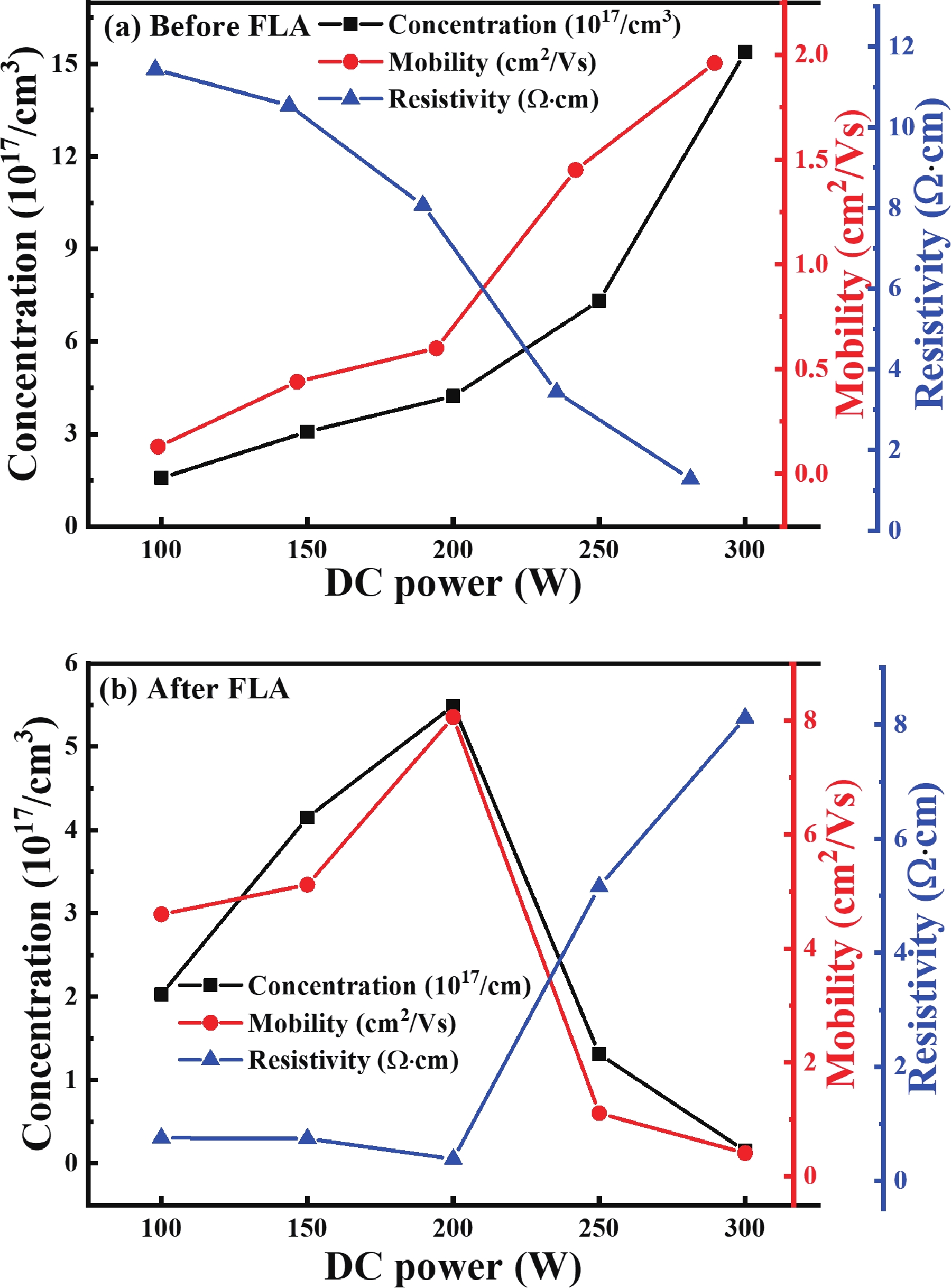
Table 1. Structural parameters of AZO thin films before and after FLA. Calculations are based on (100) peaks of the respective diffraction patterns.
| Annealing | DC sputtering power (W) | 2θ (deg) | FWHM (deg) | Area | Crystallite size (nm) | Lattice parameters | |
| a (Å) | c (Å) | ||||||
| Before FLA | 100 | 31.59 | 0.28 | 161.3 | 5.74 | 3.27 | 5.22 |
| 150 | 31.79 | 0.50 | 767.5 | 3.26 | 3.25 | 5.21 | |
| 200 | 31.99 | 0.76 | 1023.5 | 2.16 | 3.23 | 5.19 | |
| 250 | 31.92 | 0.86 | 2377.6 | 1.89 | 3.23 | 5.22 | |
| 300 | 31.70 | 0.89 | 5675.4 | 1.84 | 3.26 | 5.21 | |
| After FLA | 100 | 31.79 | 0.02 | 150.3 | 5.89 | 3.25 | 5.23 |
| 150 | 31.85 | 0.50 | 305.0 | 3.28 | 3.24 | 5.23 | |
| 200 | 31.90 | 0.73 | 2930.5 | 2.25 | 3.24 | 5.20 | |
| 250 | 31.76 | 0.78 | 4776.5 | 2.10 | 3.25 | 5.22 | |
| 300 | 31.74 | 0.69 | 8974.8 | 2.36 | 3.25 | 5.19 | |
 DownLoad: CSV
Table 2. Structural parameters of AZO thin films before and after FLA. Calculations are done by considering the (101) peak.
| Annealing | DC sputtering power (W) | 2θ (deg) | FWHM (deg) | Area | Crystallite size (nm) | Lattice parameters | |
| a (Å) | c (Å) | ||||||
| Before FLA | 100 | − | − | − | − | 3.27 | 5.22 |
| 150 | 36.29 | 0.60 | 610.1 | 2.87 | 3.25 | 5.21 | |
| 200 | 36.60 | 0.87 | 680.2 | 1.99 | 3.23 | 5.19 | |
| 250 | 36.62 | 0.87 | 711.6 | 1.98 | 3.23 | 5.22 | |
| 300 | 36.57 | 1.03 | 5337.8 | 1.68 | 3.26 | 5.21 | |
| After FLA | 100 | − | − | − | − | 3.25 | 5.23 |
| 150 | − | − | − | − | 3.24 | 5.23 | |
| 200 | 36.47 | 0.59 | 1211.2 | 2.90 | 3.24 | 5.20 | |
| 250 | 36.55 | 0.80 | 1386.3 | 2.16 | 3.25 | 5.22 | |
| 300 | 36.40 | 0.87 | 6807.2 | 1.98 | 3.25 | 5.19 | |
DownLoad: CSV
Table 3. The EDS-based atomic composition of AZO thin films after FLA.
| Element | DC power (W) | ||||
| 100 | 150 | 200 | 250 | 300 | |
| Zn | 30.9 | 32.3 | 35.6 | 24.6 | 16.6 |
| O | 44.3 | 46.7 | 46.0 | 29.4 | 24.3 |
| Al | 1.2 | 1.3 | 1.4 | 0.9 | 0.5 |
| C | 23.6 | 19.7 | 16.9 | 45.1 | 58.6 |
DownLoad: CSV
Table 4. The highest transmittance and average transmittance in visible region (400−800 nm) of AZO thin films at different DC powers before FLA and after FLA.
| Transmittance (%) | DC power (W) | ||||||||||
| Before FLA | After FLA | ||||||||||
| 100 | 150 | 200 | 250 | 300 | 100 | 150 | 200 | 250 | 300 | ||
| Highest transmittance | 93.6 | 86.3 | 82.0 | 74.1 | 60.7 | 96.0 | 94.9 | 88.5 | 61.5 | 51.3 | |
| Average transmittance | 87.1 | 80.4 | 74.5 | 62.5 | 49.0 | 90.5 | 88.4 | 80.9 | 52.4 | 43.1 | |
DownLoad: CSV
Table 5. Calculated concentration, mobility, and resistivity from Hall effect method of AZO thin films after FLA.
| Annealing | Sputtering power (W) | Concentration (1017 cm−3) | Mobility (cm2/(V·s)) | Resistivity (Ω·cm) |
| Before FLA | 100 | 1.57 | 0.13 | 11.44 |
| 150 | 3.07 | 0.44 | 10.54 | |
| 200 | 4.23 | 0.60 | 8.07 | |
| 250 | 7.32 | 1.45 | 3.43 | |
| 300 | 15.38 | 1.96 | 1.28 | |
| After FLA | 100 | 2.03 | 4.60 | 0.75 |
| 150 | 4.15 | 5.12 | 0.74 | |
| 200 | 5.49 | 8.06 | 0.38 | |
| 250 | 1.31 | 1.11 | 5.16 | |
| 300 | 0.15 | 0.41 | 8.12 |
DownLoad: CSV
Table 6. Comparison of the electrical properties of ZnO series materials after various annealing processes.
| Material | Annealing process | Concentration (cm−3) |
Mobility (cm2/(V·s)) |
Resistivity (Ω·cm) |
Reference |
| Ga-doped ZnO | Furnace annealing (FA) | 1.4 × 10²¹ | 5.3 | 8.2 × 10⁻⁴ | [66] |
| F−Ga-doped ZnO | Furnace annealing (FA) | 3.6 × 10²⁰ | 4.9 | 3.8 × 10⁻³ | [67] |
| Ti−Ga-doped ZnO | Furnace annealing (FA) | 4.0 × 10²⁰ | 6.5 | 2.2 × 10⁻³ | [68] |
| Ti-doped ZnO | Furnace annealing (FA) | 1.7 × 10²⁰ | 5.4 | 6.2 × 10⁻³ | [69] |
| Al-doped MgZnO | Rapid thermal annealing (RTA) | 1.3 × 10¹⁹ | 7.3 | 1.9 × 10³ | [70] |
| Ga-doped ZnO | Rapid thermal annealing (RTA) | 3.3 × 10²¹ | 4.6 | 5.5 × 10⁻⁴ | [71] |
| Al-doped ZnO | Rapid thermal annealing (RTA) | 5.1 × 10²⁰ | 6.8 | 1.8 × 10⁻³ | [72] |
| Al-doped ZnO | Rapid thermal annealing (RTA) | 3.9 × 10²¹ | 2.79 | 0.5 × 10⁻³ | [44] |
| Al-doped ZnO | Flash lamp annealing (FLA) | 5.4 × 10¹⁷ | 8.1 | 0.3 | This work |
DownLoad: CSV
| [1] |
Kim H, Gilmore C M, Piqué A, et al. Electrical, optical, and structural properties of indium–tin–oxide thin films for organic light-emitting devices. J Appl Phys, 1999, 86, 6451 doi: 10.1063/1.371708
|
| [2] |
Ma Z Z, Li Z R, Liu K, et al. Indium-tin-oxide for high-performance electro-optic modulation. Nanophotonics, 2015, 4, 198 doi: 10.1515/nanoph-2015-0006
|
| [3] |
Bae M S, Lee J W, Koh J H. Synthesis and characterization of multi-phase structure, optical and electrical properties on (Ga–Sn) oxide composite thin film by sol-gel method. Mater Chem Phys, 2023, 293, 126960 doi: 10.1016/j.matchemphys.2022.126960
|
| [4] |
Kokubun Y, Miura K, Endo F, et al. Sol-gel prepared β-Ga2O3 thin films for ultraviolet photodetectors. Appl Phys Lett, 2007, 90, 031912 doi: 10.1063/1.2432946
|
| [5] |
Aktas S, Caglar M. Electrical performance and HfO2 gate dielectric optimization of SnO2 thin film phototransistors. Mater Sci Eng B, 2024, 308, 117587 doi: 10.1016/j.mseb.2024.117587
|
| [6] |
Feng X Q, Cheng R Q, Yin L, et al. Two-dimensional oxide crystals for device applications: Challenges and opportunities. Adv Mater, 2024, 36, 2304708 doi: 10.1002/adma.202304708
|
| [7] |
Shoeb M, Ahmad S, Mashkoor F, et al. Investigating the size-dependent structural, optical, dielectric, and photocatalytic properties of benign-synthesized ZnO nanoparticles. J Phys Chem Solids, 2024, 184, 111707 doi: 10.1016/j.jpcs.2023.111707
|
| [8] |
Korhonen E, Tuomisto F, Gogova D, et al. Electrical compensation by Ga vacancies in Ga2O3 thin films. Appl Phys Lett, 2015, 106, 242103 doi: 10.1063/1.4922814
|
| [9] |
Teherani F H, Khodaparast G A, Xu Y V, et al. A review of the growth, doping, and applications of Beta-Ga2O3 thin films. Oxide-based Materials and Devices IX, 2018, 105330R doi: 10.1117/12.2302471
|
| [10] |
Li C T, Qiu T F, Li C, et al. Highly flexible and acid–alkali resistant TiN nanomesh transparent electrodes for next-generation optoelectronic devices. ACS Nano, 2023, 17, 24763 doi: 10.1021/acsnano.3c05211
|
| [11] |
Kim J M, Thiyagarajan P, Rhee S W. Deposition of Al-doped ZnO films on polyethylene naphthalate substrate with radio frequency magnetron sputtering. Thin Solid Films, 2010, 518, 5860 doi: 10.1016/j.tsf.2010.05.098
|
| [12] |
Yang W J, Tsao C C, Hsu C Y, et al. Fabrication and characterization of transparent conductive ZnO: Al thin films deposited on polyethylene terephthalate substrates. J Am Ceram Soc, 2012, 95, 2140 doi: 10.1111/j.1551-2916.2012.05178.x
|
| [13] |
Kim Y H, Lee J W, Murakami R I. Dependences of sputtering times on the structural and electrical properties of ZnO/Ag/ZnO thin films on PET by DC sputtering. IEEE Trans Nanotechnol, 2013, 12, 991 doi: 10.1109/TNANO.2013.2274596
|
| [14] |
Mohammed D W, Ameen R M, Waddingham R, et al. Assessing the effect of twisting and twisting fatigue on ZnO: Al thin film performance on PEN and PET substrates. Micromachines, 2024, 15, 853 doi: 10.3390/mi15070853
|
| [15] |
Akhmedov A K, Murliev E K, Asvarov A S, et al. Transparent conductive indium zinc oxide films: Temperature and oxygen dependences of the electrical and optical properties. Coatings, 2022, 12, 1583 doi: 10.3390/coatings12101583
|
| [16] |
Singh M, Scotognella F. Recent progress in solution processed aluminum and co-doped ZnO for transparent conductive oxide applications. Micromachines, 2023, 14, 536 doi: 10.3390/mi14030536
|
| [17] |
Sygletou M, Bisio F, Benedetti S, et al. Transparent conductive oxide-based architectures for the electrical modulation of the optical response: A spectroscopic ellipsometry study. J Vac Sci Technol B, 2019, 37, 061209 doi: 10.1116/1.5122175
|
| [18] |
de Oliveira G H I, Escote M T, Nantes I L, et al. Versatile r. f. magnetron sputtering doping method to produce aluminum-doped zinc oxide films. J Am Ceram Soc, 2024, 107, 4729 doi: 10.1111/jace.19753
|
| [19] |
Zhu B L, Wang C C, Xie T, et al. Highly transparent conductive ZnO films prepared by reactive RF sputtering with Zn/ZnO composite target. Appl Phys A, 2021, 127, 668 doi: 10.1007/s00339-021-04826-w
|
| [20] |
Kaneko K, Uno K, Jinno R, et al. Prospects for phase engineering of semi-stable Ga2O3 semiconductor thin films using mist chemical vapor deposition. J Appl Phys, 2022, 131, 090902 doi: 10.1063/5.0069554
|
| [21] |
Rúa A, Díaz R D, Lysenko S, et al. Semiconductor-insulator transition in VO2 (B) thin films grown by pulsed laser deposition. J Appl Phys, 2015, 118, 125308 doi: 10.1063/1.4931887
|
| [22] |
Vorobyova M, Biffoli F, Giurlani W, et al. PVD for decorative applications: A review. Materials, 2023, 16, 4919 doi: 10.3390/ma16144919
|
| [23] |
Aggarwal R, Kaushik D K. Structural and optical studies on sol-gel driven spin-coated CdS thin films. J Phys: Conf Ser, 2022, 2267, 012012 doi: 10.1088/1742-6596/2267/1/012012
|
| [24] |
Ulbrandt J G, Zhang X Z, Headrick R L, et al. Fast nonthermal processes in pulsed laser deposition. Phys Rev B, 2020, 101, 241406 doi: 10.1103/PhysRevB.101.241406
|
| [25] |
Liu H Y, Wang X Q, Li M Y, et al. Optical and electrical properties of Al doped ZnO thin film with preferred orientation in situ grown at room temperature. Ceram Int, 2019, 45, 14347 doi: 10.1016/j.ceramint.2019.04.149
|
| [26] |
Oke J A, Jen T C. Atomic layer deposition and other thin film deposition techniques: From principles to film properties. J Mater Res Technol, 2022, 21, 2481 doi: 10.1016/j.jmrt.2022.10.064
|
| [27] |
Chang S H, Koo J H, Yoo J, et al. Flexible and stretchable light-emitting diodes and photodetectors for human-centric optoelectronics. Chem Rev, 2024, 124, 768 doi: 10.1021/acs.chemrev.3c00548
|
| [28] |
Timans P, Gelpey J, McCoy S, et al. Millisecond annealing: Past, present and future. MRS Online Proc Libr, 2006, 912, 101 doi: 10.1557/PROC-0912-C01-01
|
| [29] |
Zhu M H, Liu W W, Ke W J, et al. Millisecond-pulsed photonically-annealed tin oxide electron transport layers for efficient perovskite solar cells. J Mater Chem A, 2017, 5, 24110 doi: 10.1039/C7TA07969A
|
| [30] |
Serpelloni M, Cantù E, Borghetti M, et al. Printed smart devices on cellulose-based materials by means of aerosol-jet printing and photonic curing. Sensors, 2020, 20, 841 doi: 10.3390/s20030841
|
| [31] |
Chen X B, Sastre J, Rumpel M, et al. Photonic methods for rapid crystallization of LiMn2O4 cathodes for solid-state thin-film batteries. J Power Sources, 2021, 495, 229424 doi: 10.1016/j.jpowsour.2020.229424
|
| [32] |
Jang Y R, Joo S J, Chu J H, et al. A review on intense pulsed light sintering technologies for conductive electrodes in printed electronics. Int J Precis Eng Manuf Green Technol, 2021, 8, 327 doi: 10.1007/s40684-020-00193-8
|
| [33] |
Attallah A G, Prucnal S, Buttering M, et al. Millisecond flash lamp curing for porosity generation in thin films. Sci Rep, 2023, 13, 7765 doi: 10.1038/s41598-023-34748-x
|
| [34] |
Tanimura H, Ota Y, Kawarazaki H, et al. Fabrication of thin ferroelectric Hf0.5Zr0.5O2 films by millisecond flash lamp annealing. Jpn J Appl Phys, 2023, 62, SC1044 doi: 10.35848/1347-4065/acb1b7
|
| [35] |
Jo J W, Kim K T, Park H H, et al. High-speed and low-temperature atmospheric photo-annealing of large-area solution-processed IGZO thin-film transistors by using programmable pulsed operation of xenon flash lamp. J Korean Phys Soc, 2019, 74, 1052 doi: 10.3938/jkps.74.1052
|
| [36] |
Nuchuay P, Laongwan C, Promcham W, et al. A study of the electrical and optical properties of AZO thin film by controlling pulse frequency of HiPIMS. J Met Mater Miner, 2023, 33, 103 doi: 10.55713/jmmm.v33i2.1696
|
| [37] |
Rebohle L, Prucnal S, Reichel D. Flash lamp annealing. Switzerland: Springer Cham, 2019
|
| [38] |
Zhang G X, Steuer O, Li R, et al. Al-delta-doped ZnO films made by atomic layer deposition and flash-lamp annealing for low-emissivity coating. Appl Surf Sci, 2024, 648, 159046 doi: 10.1016/j.apsusc.2023.159046
|
| [39] |
Moonen P F, Yakimets I, Huskens J. Fabrication of transistors on flexible substrates: From mass-printing to high-resolution alternative lithography strategies. Adv Mater, 2012, 24, 5526 doi: 10.1002/adma.201202949
|
| [40] |
Bae M S, Kim S H, Baek J S, et al. Comparative study of high-temperature annealed and RTA process β-Ga2O3 thin film by sol–gel process. Coatings, 2021, 11, 1220 doi: 10.3390/coatings11101220
|
| [41] |
Jun M C, Koh J H. Effects of annealing temperature on properties of Al-doped ZnO thin films prepared by sol-gel dip-coating. J Electr Eng Technol, 2013, 8, 163 doi: 10.5370/JEET.2013.8.1.163
|
| [42] |
Kim J, Ji J H, Min S W, et al. Enhanced conductance properties of UV laser/RTA annealed Al-doped ZnO thin films. Ceram Int, 2017, 43, 3900 doi: 10.1016/j.ceramint.2016.12.063
|
| [43] |
Aoun Y, Benhaoua B, Benramache S, et al. Effect of annealing temperature on structural, optical and electrical properties of zinc oxide (ZnO) thin films deposited by spray pyrolysis technique. Optik, 2015, 126, 5407 doi: 10.1016/j.ijleo.2015.08.267
|
| [44] |
Challali F, Mendil D, Touam T, et al. Effect of RF sputtering power and vacuum annealing on the properties of AZO thin films prepared from ceramic target in confocal configuration. Mater Sci Semicond Process, 2020, 118, 105217 doi: 10.1016/j.mssp.2020.105217
|
| [45] |
Lee K E, Wang M S, Kim E J, et al. Structural, electrical and optical properties of sol–gel AZO thin films. Curr Appl Phys, 2009, 9, 683 doi: 10.1016/j.cap.2008.06.006
|
| [46] |
Haider J, Rahman M, Corcoran B, et al. Simulation of thermal stress in magnetron sputtered thin coating by finite element analysis. J Mater Process Technol, 2005, 168, 36 doi: 10.1016/j.jmatprotec.2004.09.093
|
| [47] |
Park S U, Koh J H. Low temperature rf-sputtered in and Al Co-doped ZnO thin films deposited on flexible PET substrate. Ceram Int, 2014, 40, 10021 doi: 10.1016/j.ceramint.2014.02.101
|
| [48] |
Phiri R R, Oladijo O P, Akinlabi E T. Defect formation and surface evolution of thin film materials. Proceedings of the International Conference on Industrial Engineering and Operations Management, 2018, 1087
|
| [49] |
Abadias G, Chason E, Keckes J, et al. Review Article: Stress in thin films and coatings: Current status, challenges, and prospects. J Vac Sci Technol A Vac Surf Films, 2018, 36, 020801 doi: 10.1116/1.5011790
|
| [50] |
Swinehart D F. The beer-lambert law. J Chem Educ, 1962, 39, 333 doi: 10.1021/ed039p333
|
| [51] |
Park H, Qamar Hussain S, Velumani S, et al. Influence of working pressure on the structural, optical and electrical properties of sputter deposited AZO thin films. Mater Sci Semicond Process, 2015, 37, 29 doi: 10.1016/j.mssp.2014.12.076
|
| [52] |
Zhang Z Y, Bao C G, Yao W J, et al. Influence of deposition temperature on the crystallinity of Al-doped ZnO thin films at glass substrates prepared by RF magnetron sputtering method. Superlattices Microstruct, 2011, 49, 644 doi: 10.1016/j.spmi.2011.04.002
|
| [53] |
Shi Q, Zhou K S, Dai M J, et al. Room temperature preparation of high performance AZO films by MF sputtering. Ceram Int, 2013, 39, 1135 doi: 10.1016/j.ceramint.2012.07.037
|
| [54] |
He B, Xu J, Xing H Z, et al. The effect of substrate temperature on high quality c-axis oriented AZO thin films prepared by DC reactive magnetron sputtering for photoelectric device applications. Superlattices Microstruct, 2013, 64, 319 doi: 10.1016/j.spmi.2013.10.003
|
| [55] |
Zhou X F, Sun Q W, Zhai D, et al. Excellent catalytic performance of molten-salt-synthesized Bi0.5Na0.5TiO3 nanorods by the piezo-phototronic coupling effect. Nano Energy, 2021, 84, 105936 doi: 10.1016/j.nanoen.2021.105936
|
| [56] |
Constantinescu C, Matei A, Ionita I, et al. Azo-derivatives thin films grown by matrix-assisted pulsed laser evaporation for non-linear optical applications. Appl Surf Sci, 2014, 302, 69 doi: 10.1016/j.apsusc.2013.12.068
|
| [57] |
Khatami S, Fekri Aval L, Behzadi Pour G. Investigation of nanostructure and optical properties of flexible AZO thin films at different powers of RF magnetron sputtering. Nano, 2018, 13, 1850062 doi: 10.1142/S1793292018500625
|
| [58] |
Poddar N P, Mukherjee S K. Effect of substrates and post-deposition annealing on rf-sputtered Al-doped ZnO (AZO) thin films. J Mater Sci Mater Electron, 2019, 30, 14269 doi: 10.1007/s10854-019-01796-x
|
| [59] |
Islam M M, Ishizuka S, Yamada A, et al. Thickness study of Al: ZnO film for application as a window layer in Cu(In1–xGax)Se2 thin film solar cell. Appl Surf Sci, 2011, 257, 4026 doi: 10.1016/j.apsusc.2010.11.169
|
| [60] |
Poruba A, Fejfar A, Remeš Z, et al. Optical absorption and light scattering in microcrystalline silicon thin films and solar cells. J Appl Phys, 2000, 88, 148 doi: 10.1063/1.373635
|
| [61] |
Kang J, Park D, Lee D H, et al. Enhanced electrical properties of AZO/IZO multilayered thin film with post laser annealing process. J Nanosci Nanotechnol, 2021, 21, 1971 doi: 10.1166/jnn.2021.18913
|
| [62] |
Prucnal S, Rebohle L, Skorupa W. Doping by flash lamp annealing. Mater Sci Semicond Process, 2017, 62, 115 doi: 10.1016/j.mssp.2016.10.040
|
| [63] |
Skorupa W, Schumann T, Rebohle L. Millisecond thermal processing using flash lamps for the advancement of thin layers and functional coatings. Surf Coat Technol, 2017, 314, 169 doi: 10.1016/j.surfcoat.2016.08.010
|
| [64] |
Gondoni P, Ghidelli M, Di Fonzo F, et al. Structure-dependent optical and electrical transport properties of nanostructured Al-doped ZnO. Nanotechnology, 2012, 23, 365706 doi: 10.1088/0957-4484/23/36/365706
|
| [65] |
Pei Z L, Zhang X B, Zhang G P, et al. Transparent conductive ZnO: Al thin films deposited on flexible substrates prepared by direct current magnetron sputtering. Thin Solid Films, 2006, 497, 20 doi: 10.1016/j.tsf.2005.09.110
|
| [66] |
Huang C S, Liu C C. The optical and electrical properties of gallium-doped ZnO thin film with post-annealing processes of various atmospheres. Microelectron Eng, 2015, 148, 59 doi: 10.1016/j.mee.2015.08.002
|
| [67] |
Lin C L, Wang F H, Jhuang H S, et al. Effects of different annealing temperatures on the physical, optical, and electrical characteristics and chemical bonds of Ga and F Co-doped ZnO films. J Mater Res Technol, 2020, 9, 6331 doi: 10.1016/j.jmrt.2020.03.046
|
| [68] |
Chen T H, Chen T Y. Effects of annealing temperature on properties of Ti-Ga–doped ZnO films deposited on flexible substrates. Nanomaterials, 2015, 5, 1831 doi: 10.3390/nano5041831
|
| [69] |
Lin Y C, Hsu C Y, Hung S K, et al. Influence of TiO2 buffer layer and post-annealing on the quality of Ti-doped ZnO thin films. Ceram Int, 2013, 39, 5795 doi: 10.1016/j.ceramint.2012.12.099
|
| [70] |
Hsueh K P, Cheng Y C, Lin W Y, et al. High-temperature stability of postgrowth-annealed Al-doped MgxZn1-xO films without the phase separation effect. J Vac Sci Technol B, 2012, 30, 061201 doi: 10.1116/1.4754813
|
| [71] |
Horng R H, Ou S L, Huang C Y, et al. Effects of Ga concentration and rapid thermal annealing on the structural, optoelectronic and photoluminescence properties of Ga-doped ZnO thin films. Thin Solid Films, 2016, 605, 30 doi: 10.1016/j.tsf.2015.12.006
|
| [72] |
Kim D K, Kim H B. Effect of post-annealing time on the properties of sputtered Al-doped ZnO thin films. J Mater Sci Mater Electron, 2016, 27, 11366 doi: 10.1007/s10854-016-5261-3
|


Article views: 2253 Times PDF downloads: 248 Times Cited by: 0 Times
Received: 06 July 2024 Revised: 15 September 2024 Online: Accepted Manuscript: 22 October 2024Uncorrected proof: 12 November 2024Published: 15 December 2024
| Citation: |
Juwon Lee, Chang-Hyeon Jo, Gwangseop Lee, Min-Sung Bae, Slawomir Prucnal, Shengqiang Zhou, Muhammad Zubair Khan, Osama Gohar, Mohsin Saleem, Jung-Hyuk Koh. Advancing Al-doped ZnO thin films structural, optical and electrical properties of low temperature PET substrates via flash lamp annealing[J]. Journal of Semiconductors, 2024, 45(12): 122101. doi: 10.1088/1674-4926/24070005
****
J Lee, C H Jo, G Lee, M S Bae, S Prucnal, S Q Zhou, M Z Khan, O Gohar, M Saleem, and J H Koh, Advancing Al-doped ZnO thin films structural, optical and electrical properties of low temperature PET substrates via flash lamp annealing[J]. J. Semicond., 2024, 45(12), 122101 doi: 10.1088/1674-4926/24070005

|
 Juwon Lee received his Master’s degree from Chung-Ang University, South Korea in 2024. His research focuses on the study of transparent conductive oxide materials and improving properties through improving crystallinity in thin film
 Mohsin Saleem holds a Ph.D. in Electro-Functional Materials Engineering from the University of Science and Technology, South Korea. He is currently a Research Professor at the School of Electrical and Electronics Engineering, Chung-Ang University, South Korea. His research expertise lies in the field of energy storage and harvesting applications, where he focuses on developing innovative materials and technologies. Dr. Saleem has made significant contributions to the scientific community, with a strong track record of publications in high-impact journals. His work, recognized for its impact and innovation, has garnered widespread citations and recognition. He also holds patents and has presented his research at leading international conferences. Dr. Saleem is committed to advancing the field of energy solutions through interdisciplinary collaboration and cutting-edge research
 Jung-Hyuk Koh received B.S degree in Electrical Engineering from Chung-Ang University, South Korea, M.S in Advanced Materials Science and Engineering from KAIST, and Ph.D. in Sold State Electronics from Royal Insitute of Technology (KTH), Sweden. He is currently a Professor at the School of Electrical and Electronics Engineering, Chung-Ang University, South Korea. His research focuses on the piezeoelectric energy harvesting system, lead-free materials of piezoelectric, and materials of semiconductors
| [1] |
Kim H, Gilmore C M, Piqué A, et al. Electrical, optical, and structural properties of indium–tin–oxide thin films for organic light-emitting devices. J Appl Phys, 1999, 86, 6451 doi: 10.1063/1.371708
|
| [2] |
Ma Z Z, Li Z R, Liu K, et al. Indium-tin-oxide for high-performance electro-optic modulation. Nanophotonics, 2015, 4, 198 doi: 10.1515/nanoph-2015-0006
|
| [3] |
Bae M S, Lee J W, Koh J H. Synthesis and characterization of multi-phase structure, optical and electrical properties on (Ga–Sn) oxide composite thin film by sol-gel method. Mater Chem Phys, 2023, 293, 126960 doi: 10.1016/j.matchemphys.2022.126960
|
| [4] |
Kokubun Y, Miura K, Endo F, et al. Sol-gel prepared β-Ga2O3 thin films for ultraviolet photodetectors. Appl Phys Lett, 2007, 90, 031912 doi: 10.1063/1.2432946
|
| [5] |
Aktas S, Caglar M. Electrical performance and HfO2 gate dielectric optimization of SnO2 thin film phototransistors. Mater Sci Eng B, 2024, 308, 117587 doi: 10.1016/j.mseb.2024.117587
|
| [6] |
Feng X Q, Cheng R Q, Yin L, et al. Two-dimensional oxide crystals for device applications: Challenges and opportunities. Adv Mater, 2024, 36, 2304708 doi: 10.1002/adma.202304708
|
| [7] |
Shoeb M, Ahmad S, Mashkoor F, et al. Investigating the size-dependent structural, optical, dielectric, and photocatalytic properties of benign-synthesized ZnO nanoparticles. J Phys Chem Solids, 2024, 184, 111707 doi: 10.1016/j.jpcs.2023.111707
|
| [8] |
Korhonen E, Tuomisto F, Gogova D, et al. Electrical compensation by Ga vacancies in Ga2O3 thin films. Appl Phys Lett, 2015, 106, 242103 doi: 10.1063/1.4922814
|
| [9] |
Teherani F H, Khodaparast G A, Xu Y V, et al. A review of the growth, doping, and applications of Beta-Ga2O3 thin films. Oxide-based Materials and Devices IX, 2018, 105330R doi: 10.1117/12.2302471
|
| [10] |
Li C T, Qiu T F, Li C, et al. Highly flexible and acid–alkali resistant TiN nanomesh transparent electrodes for next-generation optoelectronic devices. ACS Nano, 2023, 17, 24763 doi: 10.1021/acsnano.3c05211
|
| [11] |
Kim J M, Thiyagarajan P, Rhee S W. Deposition of Al-doped ZnO films on polyethylene naphthalate substrate with radio frequency magnetron sputtering. Thin Solid Films, 2010, 518, 5860 doi: 10.1016/j.tsf.2010.05.098
|
| [12] |
Yang W J, Tsao C C, Hsu C Y, et al. Fabrication and characterization of transparent conductive ZnO: Al thin films deposited on polyethylene terephthalate substrates. J Am Ceram Soc, 2012, 95, 2140 doi: 10.1111/j.1551-2916.2012.05178.x
|
| [13] |
Kim Y H, Lee J W, Murakami R I. Dependences of sputtering times on the structural and electrical properties of ZnO/Ag/ZnO thin films on PET by DC sputtering. IEEE Trans Nanotechnol, 2013, 12, 991 doi: 10.1109/TNANO.2013.2274596
|
| [14] |
Mohammed D W, Ameen R M, Waddingham R, et al. Assessing the effect of twisting and twisting fatigue on ZnO: Al thin film performance on PEN and PET substrates. Micromachines, 2024, 15, 853 doi: 10.3390/mi15070853
|
| [15] |
Akhmedov A K, Murliev E K, Asvarov A S, et al. Transparent conductive indium zinc oxide films: Temperature and oxygen dependences of the electrical and optical properties. Coatings, 2022, 12, 1583 doi: 10.3390/coatings12101583
|
| [16] |
Singh M, Scotognella F. Recent progress in solution processed aluminum and co-doped ZnO for transparent conductive oxide applications. Micromachines, 2023, 14, 536 doi: 10.3390/mi14030536
|
| [17] |
Sygletou M, Bisio F, Benedetti S, et al. Transparent conductive oxide-based architectures for the electrical modulation of the optical response: A spectroscopic ellipsometry study. J Vac Sci Technol B, 2019, 37, 061209 doi: 10.1116/1.5122175
|
| [18] |
de Oliveira G H I, Escote M T, Nantes I L, et al. Versatile r. f. magnetron sputtering doping method to produce aluminum-doped zinc oxide films. J Am Ceram Soc, 2024, 107, 4729 doi: 10.1111/jace.19753
|
| [19] |
Zhu B L, Wang C C, Xie T, et al. Highly transparent conductive ZnO films prepared by reactive RF sputtering with Zn/ZnO composite target. Appl Phys A, 2021, 127, 668 doi: 10.1007/s00339-021-04826-w
|
| [20] |
Kaneko K, Uno K, Jinno R, et al. Prospects for phase engineering of semi-stable Ga2O3 semiconductor thin films using mist chemical vapor deposition. J Appl Phys, 2022, 131, 090902 doi: 10.1063/5.0069554
|
| [21] |
Rúa A, Díaz R D, Lysenko S, et al. Semiconductor-insulator transition in VO2 (B) thin films grown by pulsed laser deposition. J Appl Phys, 2015, 118, 125308 doi: 10.1063/1.4931887
|
| [22] |
Vorobyova M, Biffoli F, Giurlani W, et al. PVD for decorative applications: A review. Materials, 2023, 16, 4919 doi: 10.3390/ma16144919
|
| [23] |
Aggarwal R, Kaushik D K. Structural and optical studies on sol-gel driven spin-coated CdS thin films. J Phys: Conf Ser, 2022, 2267, 012012 doi: 10.1088/1742-6596/2267/1/012012
|
| [24] |
Ulbrandt J G, Zhang X Z, Headrick R L, et al. Fast nonthermal processes in pulsed laser deposition. Phys Rev B, 2020, 101, 241406 doi: 10.1103/PhysRevB.101.241406
|
| [25] |
Liu H Y, Wang X Q, Li M Y, et al. Optical and electrical properties of Al doped ZnO thin film with preferred orientation in situ grown at room temperature. Ceram Int, 2019, 45, 14347 doi: 10.1016/j.ceramint.2019.04.149
|
| [26] |
Oke J A, Jen T C. Atomic layer deposition and other thin film deposition techniques: From principles to film properties. J Mater Res Technol, 2022, 21, 2481 doi: 10.1016/j.jmrt.2022.10.064
|
| [27] |
Chang S H, Koo J H, Yoo J, et al. Flexible and stretchable light-emitting diodes and photodetectors for human-centric optoelectronics. Chem Rev, 2024, 124, 768 doi: 10.1021/acs.chemrev.3c00548
|
| [28] |
Timans P, Gelpey J, McCoy S, et al. Millisecond annealing: Past, present and future. MRS Online Proc Libr, 2006, 912, 101 doi: 10.1557/PROC-0912-C01-01
|
| [29] |
Zhu M H, Liu W W, Ke W J, et al. Millisecond-pulsed photonically-annealed tin oxide electron transport layers for efficient perovskite solar cells. J Mater Chem A, 2017, 5, 24110 doi: 10.1039/C7TA07969A
|
| [30] |
Serpelloni M, Cantù E, Borghetti M, et al. Printed smart devices on cellulose-based materials by means of aerosol-jet printing and photonic curing. Sensors, 2020, 20, 841 doi: 10.3390/s20030841
|
| [31] |
Chen X B, Sastre J, Rumpel M, et al. Photonic methods for rapid crystallization of LiMn2O4 cathodes for solid-state thin-film batteries. J Power Sources, 2021, 495, 229424 doi: 10.1016/j.jpowsour.2020.229424
|
| [32] |
Jang Y R, Joo S J, Chu J H, et al. A review on intense pulsed light sintering technologies for conductive electrodes in printed electronics. Int J Precis Eng Manuf Green Technol, 2021, 8, 327 doi: 10.1007/s40684-020-00193-8
|
| [33] |
Attallah A G, Prucnal S, Buttering M, et al. Millisecond flash lamp curing for porosity generation in thin films. Sci Rep, 2023, 13, 7765 doi: 10.1038/s41598-023-34748-x
|
| [34] |
Tanimura H, Ota Y, Kawarazaki H, et al. Fabrication of thin ferroelectric Hf0.5Zr0.5O2 films by millisecond flash lamp annealing. Jpn J Appl Phys, 2023, 62, SC1044 doi: 10.35848/1347-4065/acb1b7
|
| [35] |
Jo J W, Kim K T, Park H H, et al. High-speed and low-temperature atmospheric photo-annealing of large-area solution-processed IGZO thin-film transistors by using programmable pulsed operation of xenon flash lamp. J Korean Phys Soc, 2019, 74, 1052 doi: 10.3938/jkps.74.1052
|
| [36] |
Nuchuay P, Laongwan C, Promcham W, et al. A study of the electrical and optical properties of AZO thin film by controlling pulse frequency of HiPIMS. J Met Mater Miner, 2023, 33, 103 doi: 10.55713/jmmm.v33i2.1696
|
| [37] |
Rebohle L, Prucnal S, Reichel D. Flash lamp annealing. Switzerland: Springer Cham, 2019
|
| [38] |
Zhang G X, Steuer O, Li R, et al. Al-delta-doped ZnO films made by atomic layer deposition and flash-lamp annealing for low-emissivity coating. Appl Surf Sci, 2024, 648, 159046 doi: 10.1016/j.apsusc.2023.159046
|
| [39] |
Moonen P F, Yakimets I, Huskens J. Fabrication of transistors on flexible substrates: From mass-printing to high-resolution alternative lithography strategies. Adv Mater, 2012, 24, 5526 doi: 10.1002/adma.201202949
|
| [40] |
Bae M S, Kim S H, Baek J S, et al. Comparative study of high-temperature annealed and RTA process β-Ga2O3 thin film by sol–gel process. Coatings, 2021, 11, 1220 doi: 10.3390/coatings11101220
|
| [41] |
Jun M C, Koh J H. Effects of annealing temperature on properties of Al-doped ZnO thin films prepared by sol-gel dip-coating. J Electr Eng Technol, 2013, 8, 163 doi: 10.5370/JEET.2013.8.1.163
|
| [42] |
Kim J, Ji J H, Min S W, et al. Enhanced conductance properties of UV laser/RTA annealed Al-doped ZnO thin films. Ceram Int, 2017, 43, 3900 doi: 10.1016/j.ceramint.2016.12.063
|
| [43] |
Aoun Y, Benhaoua B, Benramache S, et al. Effect of annealing temperature on structural, optical and electrical properties of zinc oxide (ZnO) thin films deposited by spray pyrolysis technique. Optik, 2015, 126, 5407 doi: 10.1016/j.ijleo.2015.08.267
|
| [44] |
Challali F, Mendil D, Touam T, et al. Effect of RF sputtering power and vacuum annealing on the properties of AZO thin films prepared from ceramic target in confocal configuration. Mater Sci Semicond Process, 2020, 118, 105217 doi: 10.1016/j.mssp.2020.105217
|
| [45] |
Lee K E, Wang M S, Kim E J, et al. Structural, electrical and optical properties of sol–gel AZO thin films. Curr Appl Phys, 2009, 9, 683 doi: 10.1016/j.cap.2008.06.006
|
| [46] |
Haider J, Rahman M, Corcoran B, et al. Simulation of thermal stress in magnetron sputtered thin coating by finite element analysis. J Mater Process Technol, 2005, 168, 36 doi: 10.1016/j.jmatprotec.2004.09.093
|
| [47] |
Park S U, Koh J H. Low temperature rf-sputtered in and Al Co-doped ZnO thin films deposited on flexible PET substrate. Ceram Int, 2014, 40, 10021 doi: 10.1016/j.ceramint.2014.02.101
|
| [48] |
Phiri R R, Oladijo O P, Akinlabi E T. Defect formation and surface evolution of thin film materials. Proceedings of the International Conference on Industrial Engineering and Operations Management, 2018, 1087
|
| [49] |
Abadias G, Chason E, Keckes J, et al. Review Article: Stress in thin films and coatings: Current status, challenges, and prospects. J Vac Sci Technol A Vac Surf Films, 2018, 36, 020801 doi: 10.1116/1.5011790
|
| [50] |
Swinehart D F. The beer-lambert law. J Chem Educ, 1962, 39, 333 doi: 10.1021/ed039p333
|
| [51] |
Park H, Qamar Hussain S, Velumani S, et al. Influence of working pressure on the structural, optical and electrical properties of sputter deposited AZO thin films. Mater Sci Semicond Process, 2015, 37, 29 doi: 10.1016/j.mssp.2014.12.076
|
| [52] |
Zhang Z Y, Bao C G, Yao W J, et al. Influence of deposition temperature on the crystallinity of Al-doped ZnO thin films at glass substrates prepared by RF magnetron sputtering method. Superlattices Microstruct, 2011, 49, 644 doi: 10.1016/j.spmi.2011.04.002
|
| [53] |
Shi Q, Zhou K S, Dai M J, et al. Room temperature preparation of high performance AZO films by MF sputtering. Ceram Int, 2013, 39, 1135 doi: 10.1016/j.ceramint.2012.07.037
|
| [54] |
He B, Xu J, Xing H Z, et al. The effect of substrate temperature on high quality c-axis oriented AZO thin films prepared by DC reactive magnetron sputtering for photoelectric device applications. Superlattices Microstruct, 2013, 64, 319 doi: 10.1016/j.spmi.2013.10.003
|
| [55] |
Zhou X F, Sun Q W, Zhai D, et al. Excellent catalytic performance of molten-salt-synthesized Bi0.5Na0.5TiO3 nanorods by the piezo-phototronic coupling effect. Nano Energy, 2021, 84, 105936 doi: 10.1016/j.nanoen.2021.105936
|
| [56] |
Constantinescu C, Matei A, Ionita I, et al. Azo-derivatives thin films grown by matrix-assisted pulsed laser evaporation for non-linear optical applications. Appl Surf Sci, 2014, 302, 69 doi: 10.1016/j.apsusc.2013.12.068
|
| [57] |
Khatami S, Fekri Aval L, Behzadi Pour G. Investigation of nanostructure and optical properties of flexible AZO thin films at different powers of RF magnetron sputtering. Nano, 2018, 13, 1850062 doi: 10.1142/S1793292018500625
|
| [58] |
Poddar N P, Mukherjee S K. Effect of substrates and post-deposition annealing on rf-sputtered Al-doped ZnO (AZO) thin films. J Mater Sci Mater Electron, 2019, 30, 14269 doi: 10.1007/s10854-019-01796-x
|
| [59] |
Islam M M, Ishizuka S, Yamada A, et al. Thickness study of Al: ZnO film for application as a window layer in Cu(In1–xGax)Se2 thin film solar cell. Appl Surf Sci, 2011, 257, 4026 doi: 10.1016/j.apsusc.2010.11.169
|
| [60] |
Poruba A, Fejfar A, Remeš Z, et al. Optical absorption and light scattering in microcrystalline silicon thin films and solar cells. J Appl Phys, 2000, 88, 148 doi: 10.1063/1.373635
|
| [61] |
Kang J, Park D, Lee D H, et al. Enhanced electrical properties of AZO/IZO multilayered thin film with post laser annealing process. J Nanosci Nanotechnol, 2021, 21, 1971 doi: 10.1166/jnn.2021.18913
|
| [62] |
Prucnal S, Rebohle L, Skorupa W. Doping by flash lamp annealing. Mater Sci Semicond Process, 2017, 62, 115 doi: 10.1016/j.mssp.2016.10.040
|
| [63] |
Skorupa W, Schumann T, Rebohle L. Millisecond thermal processing using flash lamps for the advancement of thin layers and functional coatings. Surf Coat Technol, 2017, 314, 169 doi: 10.1016/j.surfcoat.2016.08.010
|
| [64] |
Gondoni P, Ghidelli M, Di Fonzo F, et al. Structure-dependent optical and electrical transport properties of nanostructured Al-doped ZnO. Nanotechnology, 2012, 23, 365706 doi: 10.1088/0957-4484/23/36/365706
|
| [65] |
Pei Z L, Zhang X B, Zhang G P, et al. Transparent conductive ZnO: Al thin films deposited on flexible substrates prepared by direct current magnetron sputtering. Thin Solid Films, 2006, 497, 20 doi: 10.1016/j.tsf.2005.09.110
|
| [66] |
Huang C S, Liu C C. The optical and electrical properties of gallium-doped ZnO thin film with post-annealing processes of various atmospheres. Microelectron Eng, 2015, 148, 59 doi: 10.1016/j.mee.2015.08.002
|
| [67] |
Lin C L, Wang F H, Jhuang H S, et al. Effects of different annealing temperatures on the physical, optical, and electrical characteristics and chemical bonds of Ga and F Co-doped ZnO films. J Mater Res Technol, 2020, 9, 6331 doi: 10.1016/j.jmrt.2020.03.046
|
| [68] |
Chen T H, Chen T Y. Effects of annealing temperature on properties of Ti-Ga–doped ZnO films deposited on flexible substrates. Nanomaterials, 2015, 5, 1831 doi: 10.3390/nano5041831
|
| [69] |
Lin Y C, Hsu C Y, Hung S K, et al. Influence of TiO2 buffer layer and post-annealing on the quality of Ti-doped ZnO thin films. Ceram Int, 2013, 39, 5795 doi: 10.1016/j.ceramint.2012.12.099
|
| [70] |
Hsueh K P, Cheng Y C, Lin W Y, et al. High-temperature stability of postgrowth-annealed Al-doped MgxZn1-xO films without the phase separation effect. J Vac Sci Technol B, 2012, 30, 061201 doi: 10.1116/1.4754813
|
| [71] |
Horng R H, Ou S L, Huang C Y, et al. Effects of Ga concentration and rapid thermal annealing on the structural, optoelectronic and photoluminescence properties of Ga-doped ZnO thin films. Thin Solid Films, 2016, 605, 30 doi: 10.1016/j.tsf.2015.12.006
|
| [72] |
Kim D K, Kim H B. Effect of post-annealing time on the properties of sputtered Al-doped ZnO thin films. J Mater Sci Mater Electron, 2016, 27, 11366 doi: 10.1007/s10854-016-5261-3
|

 WeChat ID
Journal of Semiconductors © 2017 All Rights Reserved 京ICP备05085259号-2


