


Fig. 1.
(Color online) (a) Quantum well structure diagram. (b) Hall bar structure diagram and test schematic diagram.
ARTICLES
Yiwen Zhang1, 2, 3, 4, Jun Deng4, Zonghu Li4, Xinyou Liu4, Haiou Li4, 5, Baochuan Wang4, 5, Jun Luo2, 3, Zhenzhen Kong2, 3, , Gang Cao4, 5, Guoping Guo4, 5, Chao Zhao3 and Guilei Wang2, 4,
Corresponding author: Zhenzhen Kong, zhenzhen.kong@bjsamt.org.cn; Guilei Wang, wangguilei@hfnl.cn
Abstract: Ge/SiGe heterostructure quantum wells play a pivotal role in the pursuit of scalable silicon-based qubits. The varying compressive strains within these quantum wells profoundly influence the physical characteristics of the qubits, yet this factor remains largely unexplored, driving our research endeavor. In this study, we utilized RP-CVD (Reduced Pressure Chemical Vapor Deposition) to grow Ge quantum wells with varied compressive strain, proposing growth schemes for lightly-strained (ε∥ = −0.43%) QW (quantum well), standard-strained (ε∥ = −0.61%) QW, and heavily-strained (ε∥ = −1.19%) QW. Through comprehensive material characterization, particularly employing the low-temperature magneto-transport measurements, we derived the percolation densities ranging from 4.7 × 10¹⁰ to 14.2 × 1010 cm−2 and mobilities from 3.382 × 10⁵ to 7.301 × 105 cm2∙V−1∙s−1. Combined with the first-principles calculations, our analysis delves into the trends in effective mass and percolation density at low temperatures, shedding light on the impact of quantum effects on band structures and the interplay between structural components and wave functions. This research offers a comprehensive investigation into the intrinsic mechanisms governing complex multi-strained quantum wells, spanning growth, characterization, and computational perspectives, thereby establishing a strategy for the growth of high-quality strained quantum wells.
Keywords: germanium quantum wells, RP-CVD, multi-strained quantum wells, magneto-transport, hetero-structure
| [1] |
Liu Y, Xiong J X, Wang Z, et al. Electric dipole spin resonance induced by hole k-linear Rashba effect in planar Ge. arXiv preprint arXiv: 2106.14684, 2021
|
| [2] |
Zhao C, Wang X, Wang W. High-κ dielectric and metal gate. CMOS Past, Present and Future. Amsterdam: Elsevier, 2018, 69
|
| [3] |
Scappucci G, Kloeffel C, Zwanenburg F A, et al. The germanium quantum information route. Nat Rev Mater, 2021, 6, 926 doi: 10.1038/s41578-020-00262-z
|
| [4] |
Lodari M, Kong O, Rendell M, et al. Lightly strained germanium quantum wells with hole mobility exceeding one million. Appl Phys Lett, 2022, 120, 122104 doi: 10.1063/5.0083161
|
| [5] |
Myronov M, Kycia J, Waldron P, et al. Holes outperform electrons in group IV semiconductor materials. Small Sci, 2023, 3, 2200094 doi: 10.1002/smsc.202200094
|
| [6] |
Hutchins-Delgado T A, Miller A J, Scott R, et al. Characterization of shallow, undoped Ge/SiGe quantum wells commercially grown on 8-in. (100) Si wafers. ACS Appl Electron Mater, 2022, 4, 4482 doi: 10.1021/acsaelm.2c00733
|
| [7] |
Kong Z, Li Z, Cao G, et al. Undoped strained Ge quantum well with ultrahigh mobility of two million. ACS Appl Mater Interfaces, 2023, 15, 28799 doi: 10.1021/acsami.3c03294
|
| [8] |
Stehouwer L E A, Tosato A, Degli Esposti D, et al. Germanium wafers for strained quantum wells with low disorder. Appl Phys Lett, 2023, 123, 092101 doi: 10.1063/5.0158262
|
| [9] |
Sammak A, Sabbagh D, Hendrickx N W, et al. Shallow and undoped germanium quantum wells: A playground for spin and hybrid quantum technology. Adv Funct Mater, 2019, 29, 1807613 doi: 10.1002/adfm.201807613
|
| [10] |
Hendrickx N W, Lawrie W I L, Russ M, et al. A four-qubit germanium quantum processor. Nature, 2021, 591, 580 doi: 10.1038/s41586-021-03332-6
|
| [11] |
Li Y X, Kong Z Z, Hou S M, et al. Quantum transport quality of a processed undoped Ge/SiGe heterostructure. Phys Rev B, 2023, 108, 045303 doi: 10.1103/PhysRevB.108.045303
|
| [12] |
Ma R L, Li A R, Wang C, et al. Single-spin-qubit geometric gate in a silicon quantum dot. Phys Rev Applied, 2024, 21, 014044 doi: 10.1103/PhysRevApplied.21.014044
|
| [13] |
Yoneda J, Takeda K, Otsuka T, et al. A quantum-dot spin qubit with coherence limited by charge noise and fidelity higher than 99.9. Nat Nanotechnol, 2018, 13, 102 doi: 10.1038/s41565-017-0014-x
|
| [14] |
Hardy W J, Harris C T, Su Y H, et al. Single and double hole quantum dots in strained Ge/SiGe quantum wells. Nanotechnology, 2019, 30, 215202 doi: 10.1088/1361-6528/ab061e
|
| [15] |
Terrazos L A, Marcellina E, Wang Z N, et al. Theory of hole-spin qubits in strained germanium quantum dots. Phys Rev B, 2021, 103, 125201 doi: 10.1103/PhysRevB.103.125201
|
| [16] |
Zhang D D, Lu J, Liu Z, et al. Sharp interface of undoped Ge/SiGe quantum well grown by ultrahigh vacuum chemical vapor deposition. Appl Phys Lett, 2022, 121, 022102 doi: 10.1063/5.0097846
|
| [17] |
Kang Y, Li Z H, Kong Z Z, et al. Coupling of a hole double quantum dot in planar germanium to a microwave cavity. Phys Rev Applied, 2024, 22, 024054 doi: 10.1103/PhysRevApplied.22.024054
|
| [18] |
Jirovec D, Hofmann A, Ballabio A, et al. A singlet-triplet hole spin qubit in planar Ge. Nat Mater, 2021, 20, 1106 doi: 10.1038/s41563-021-01022-2
|
| [19] |
Zhang Y W, Li Z H, Zhou Y C, et al. Ultrashallow heavily constrained quantum wells: The cradle for fully electrically controlled and microwave coupled quantum bits. Phys Rev Materials, 2024, 8, 046203 doi: 10.1103/PhysRevMaterials.8.046203
|
| [20] |
Berkutov I B, Andrievskii V V, Beliayev E Y, et al. Quantum effects in silicon-germanium p-type heterostructures with quantum wells of different widths. Low Temp Phys, 2023, 49, 59 doi: 10.1063/10.0016476
|
| [21] |
Laroche D, Huang S H, Chuang Y, et al. Magneto-transport analysis of an ultra-low-density two-dimensional hole gas in an undoped strained Ge/SiGe heterostructure. Appl Phys Lett, 2016, 108, 233504 doi: 10.1063/1.4953399
|
| [22] |
Su Y H, Chuang Y, Liu C Y, et al. Effects of surface tunneling of two-dimensional hole gases in undoped Ge/GeSi heterostructures. Phys Rev Materials, 2017, 1, 044601 doi: 10.1103/PhysRevMaterials.1.044601
|
| [23] |
Hartmann J M, Damlencourt J F, Bogumilowicz Y, et al. Reduced pressure-chemical vapor deposition of intrinsic and doped Ge layers on Si(001) for microelectronics and optoelectronics purposes. J Cryst Growth, 2005, 274, 90 doi: 10.1016/j.jcrysgro.2004.10.042
|
| [24] |
Newell O. Fractional quantum phenomena of 2DHGs within strained germanium quantum well heterostructures. University of Warwick, 2018
|
| [25] |
Ward T, Sánchez A M, Tang M, et al. Design rules for dislocation filters. J Appl Phys, 2014, 116, 063508 doi: 10.1063/1.4892162
|
| [26] |
Fitzgerald E A. Dislocations in strained-layer epitaxy: Theory, experiment, and applications. Mater Sci Rep, 1991, 7, 87 doi: 10.1016/0920-2307(91)90006-9
|
| [27] |
Ballabio A, Frigerio J, Firoozabadi S, et al. Ge/SiGe parabolic quantum wells. J Phys D: Appl Phys, 2019, 52, 415105 doi: 10.1088/1361-6463/ab2d34
|
| [28] |
Alam M M, Hoshi Y, Sawano K. Structural properties of compressive strained Ge channels fabricated on Si (111) and Si (100). Semicond Sci Technol, 2018, 33, 124008 doi: 10.1088/1361-6641/aae575
|
| [29] |
Skibitzki O, Zoellner M H, Rovaris F, et al. Reduction of threading dislocation density beyond the saturation limit by optimized reverse grading. Phys Rev Materials, 2020, 4, 103403 doi: 10.1103/PhysRevMaterials.4.103403
|
| [30] |
Cheng W J, Liang R R, Xu G B, et al. Fabrication and characterization of a novel Si line tunneling TFET with high drive current. IEEE J Electron Devices Soc, 2826, 8, 336 doi: 10.1109/JEDS.2020.2981974
|
| [31] |
Wang G L, Luo J, Qin C L, et al. Integration of highly strained SiGe in source and drain with HK and MG for 22 nm bulk PMOS transistors. Nanoscale Res Lett, 2017, 12, 123 doi: 10.1186/s11671-017-1908-0
|
| [32] |
von Känel H, Kummer M, Isella G, et al. Very high hole mobilities in modulation-doped Ge quantum wells grown by low-energy plasma enhanced chemical vapor deposition. Appl Phys Lett, 2002, 80, 2922 doi: 10.1063/1.1470691
|
| [33] |
Rößner B, Isella G, von Känel H. Effective mass in remotely doped Ge quantum wells. Appl Phys Lett, 2003, 82, 754 doi: 10.1063/1.1541101
|
| [34] |
Pokutnyi S I. Polarizability of germanium quantum dots with spatially separated electrons and holes. Eur Phys J Plus, 2020, 135, 74 doi: 10.1140/epjp/s13360-019-00050-x
|
| [35] |
Rančić M J, Hoffman S, Schrade C, et al. Entangling spins in double quantum dots and Majorana bound states. Phys Rev B, 2019, 99, 165306 doi: 10.1103/PhysRevB.99.165306
|
| [36] |
Del Vecchio P, Lodari M, Sammak A, et al. Vanishing Zeeman energy in a two-dimensional hole gas. Phys Rev B, 2020, 102, 115304 doi: 10.1103/PhysRevB.102.115304
|
| [37] |
Coleridge P T, Stoner R, Fletcher R. Low-field transport coefficients in GaAs/Ga1–xAlxAs heterostructures. Phys Rev B, 1989, 39, 1120 doi: 10.1103/PhysRevB.39.1120
|
| [38] |
Winkler R, Papadakis S J, Poortere E P, et al. Spin-orbit coupling in two-dimensional electron and hole systems. Advances in Solid State Physics Volume 41. Berlin, Heidelberg: Springer Berlin Heidelberg, 2007, 211
|
| [39] |
Miller A J, Brickson M, Hardy W J, et al. Effective out-of-plane g-factor in strained-Ge/SiGe quantum dots. Phys Rev B, 2022, 106, 121402 doi: 10.1103/PhysRevB.106.L121402
|
| [40] |
Drichko I L, Dmitriev A A, Malysh V A, et al. Effective g factor of 2D holes in strained Ge quantum wells. J Appl Phys, 2018, 123, 165703 doi: 10.1063/1.5025413
|
| [41] |
Mizokuchi R, Maurand R, Vigneau F, et al. Ballistic one-dimensional holes with strong g-factor anisotropy in germanium. Nano Lett, 2018, 18, 4861 doi: 10.1021/acs.nanolett.8b01457
|
| [42] |
Ma J L, Zhang H M, Wang X Y, et al. Valence band structure and hole effective mass of uniaxial stressed Germanium. J Comput Electron, 2011, 10, 388 doi: 10.1007/s10825-011-0374-7
|
| [43] |
Virgilio M, Grosso G. Type-I alignment and direct fundamental gap in SiGe based heterostructures. J Phys Condens Matter, 2006, 18, 1021 doi: 10.1088/0953-8984/18/3/018
|
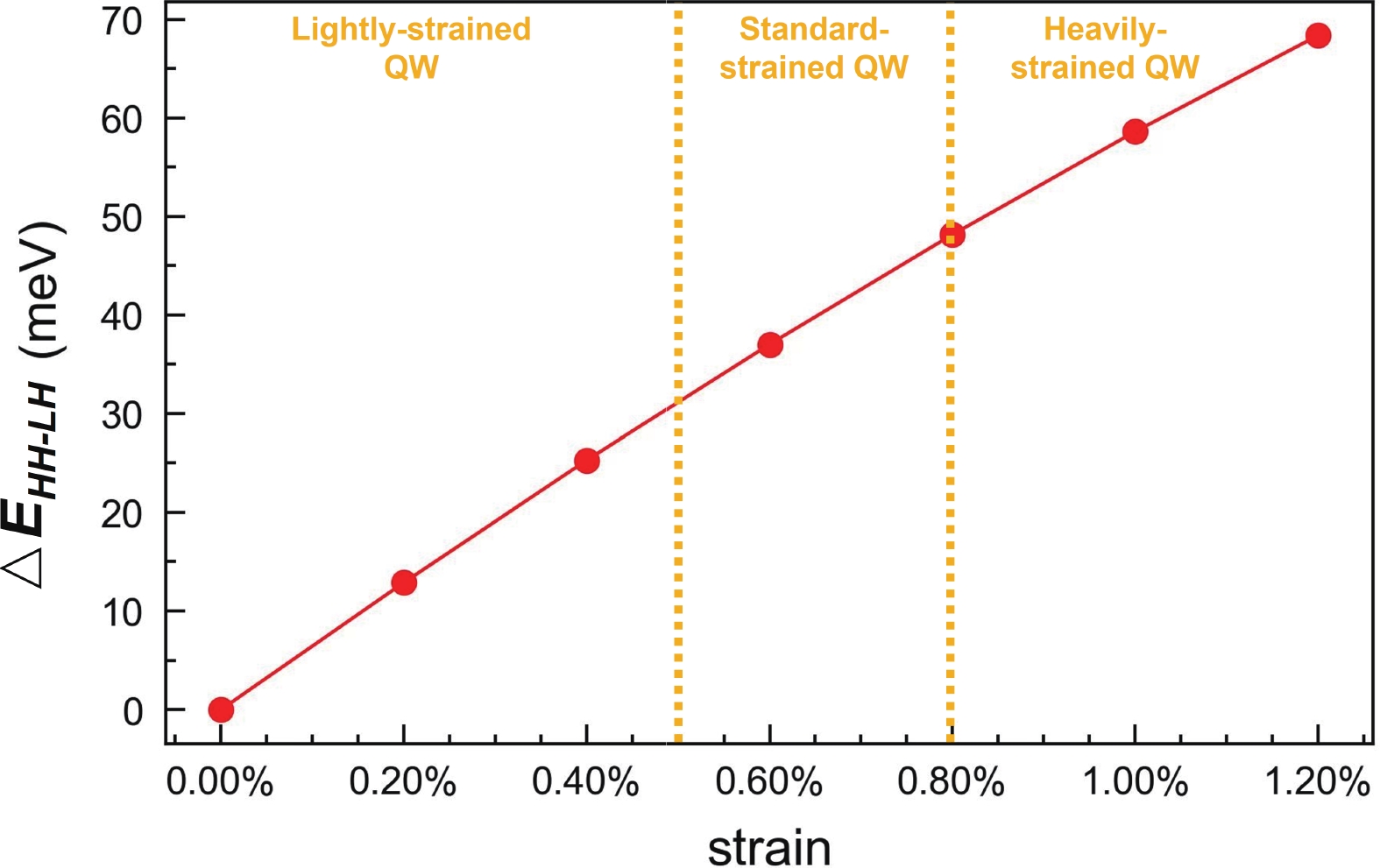
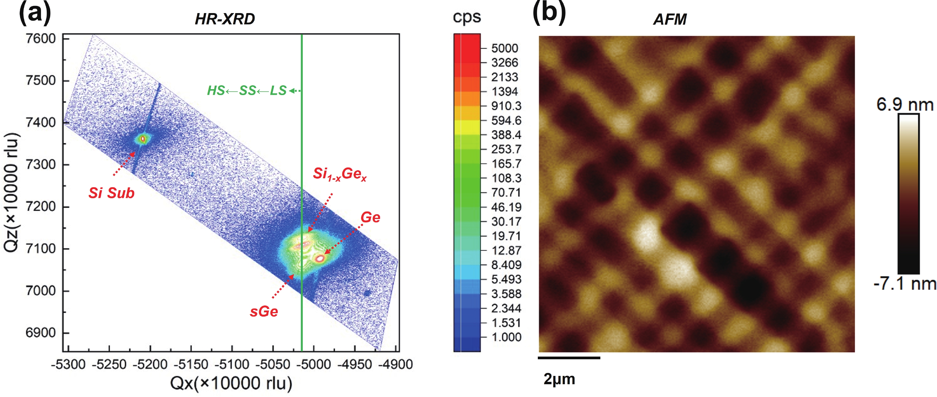
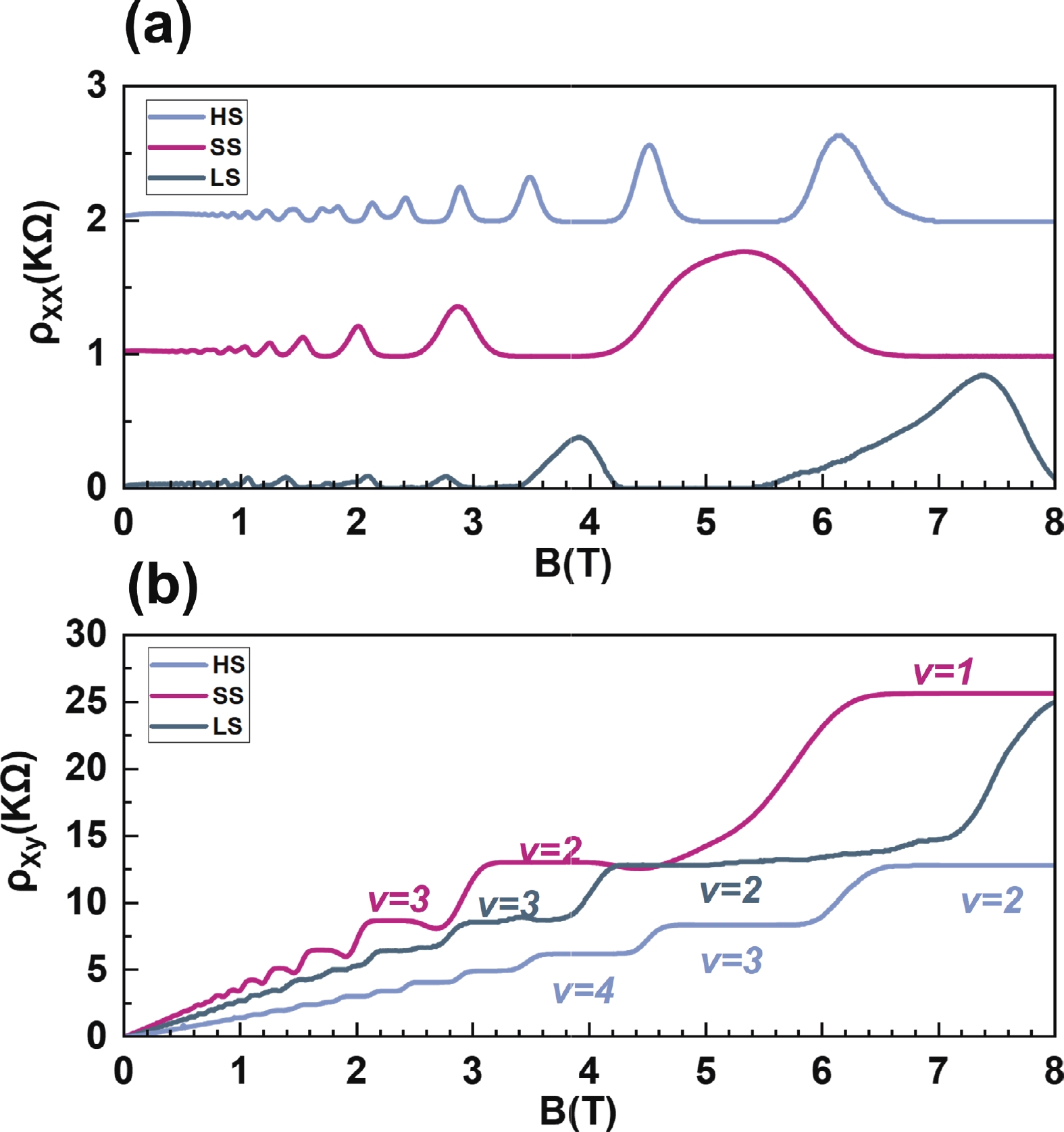
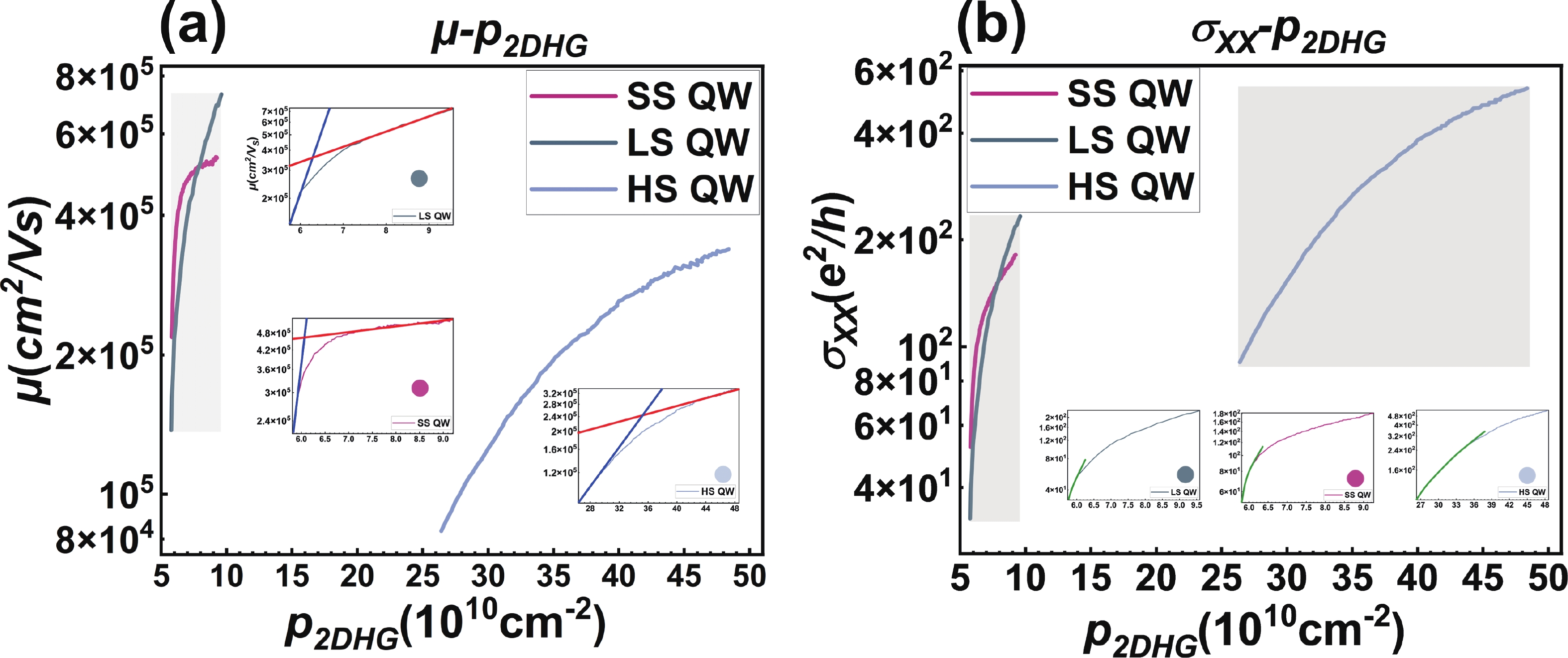
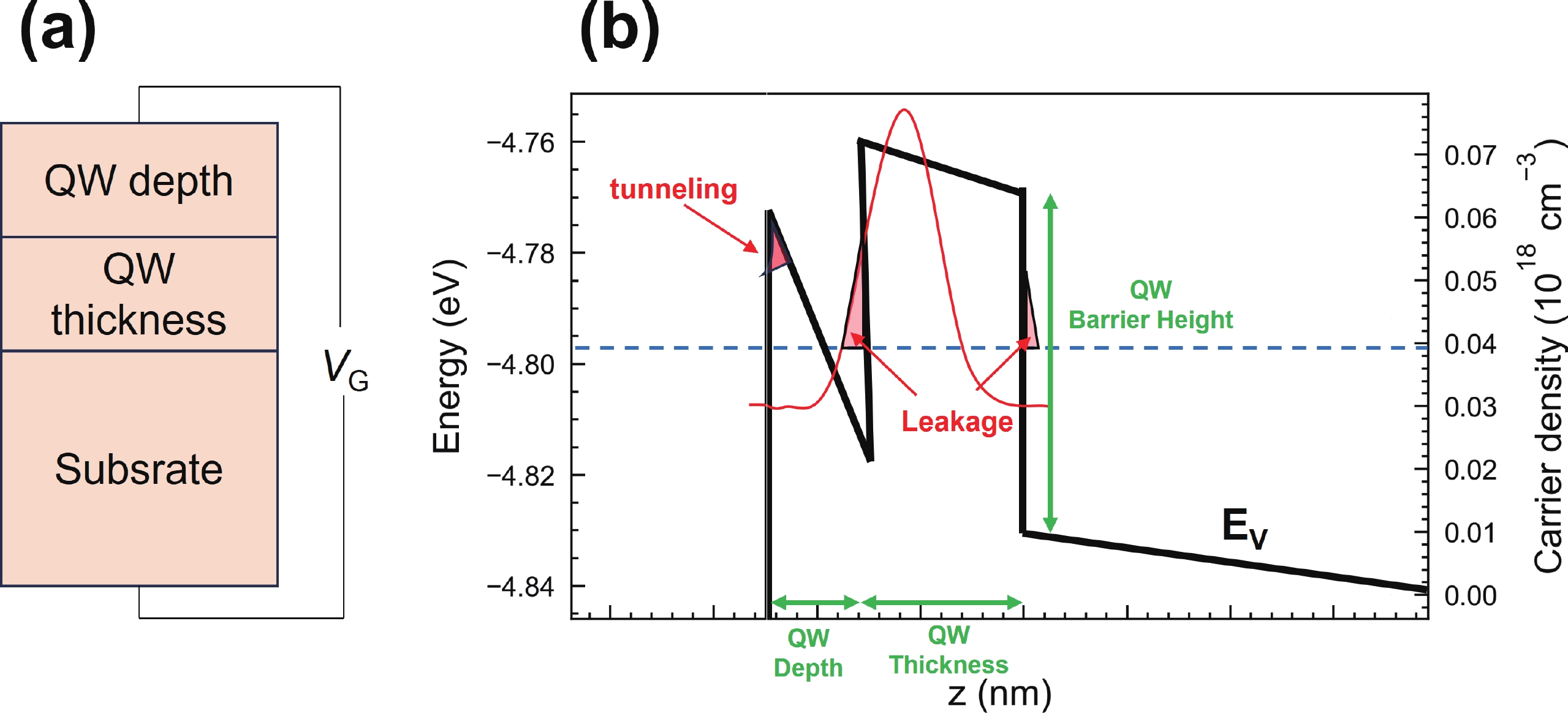

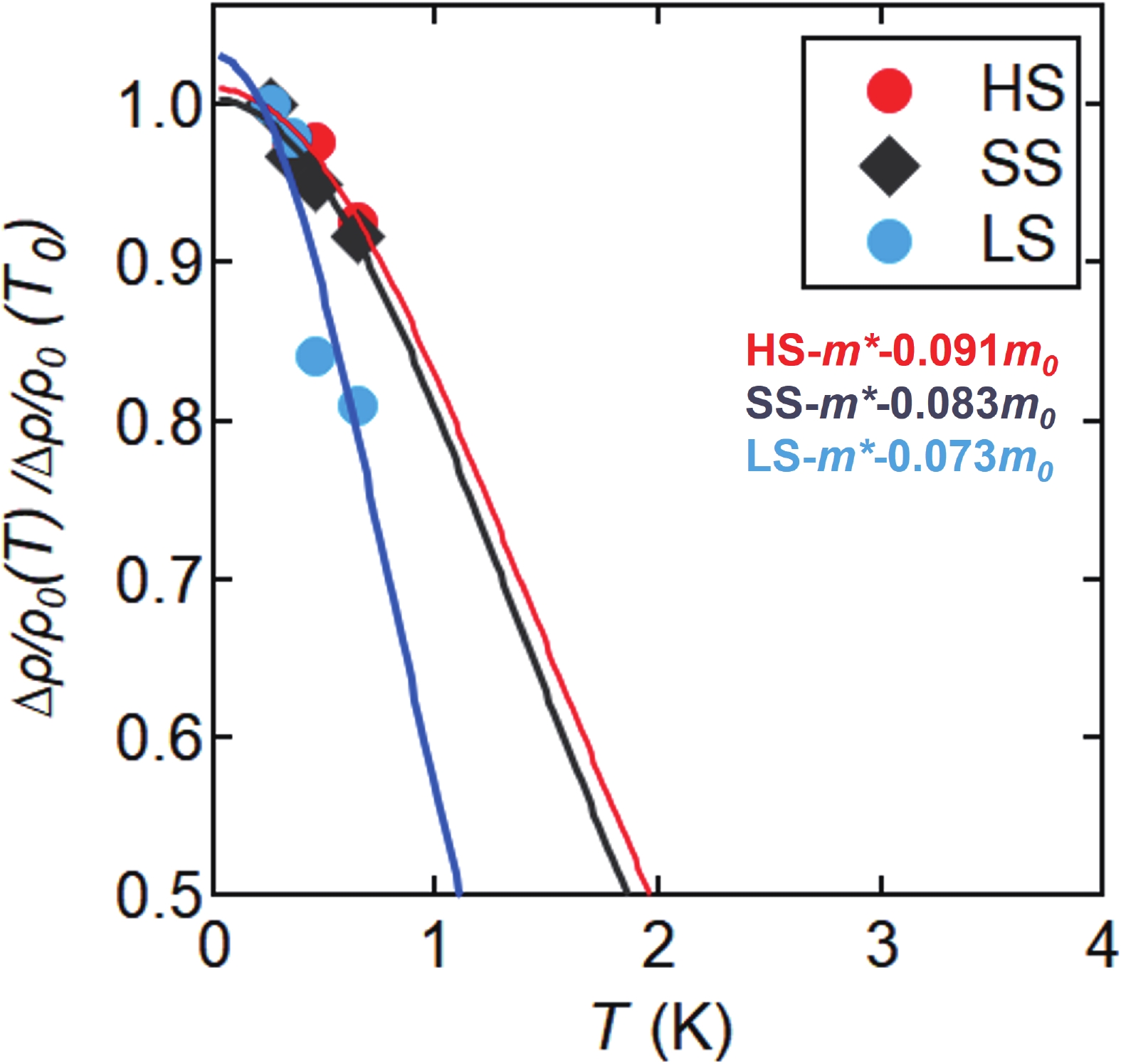
Table 1. Material key structural parameters and magnetic transport test results.
| Key structural parameters | |||
| Layer | LS QW | SS QW | HS QW |
| QW depth (nm) | 22.7 | 20.2 | 15.1 |
| QW thickness (nm) | 37 | 36.3 | 24.07 |
| Strain (%) | −0.43 | −0.61 | −1.19 |
| Magnetic-transport data | |||
| Layer | LS QW | SS QW | HS QW |
| Mobility (cm2∙V−1∙s−1) | 73.01 × 10⁴ | 53.47 × 10⁴ | 33.82 × 10⁴ |
| βhigh | 2.18 | 0.40 | 1.27 |
| βlow | 11.51 | 16.95 | 3.46 |
| m* (m0) | 0.073 | 0.083 | 0.091 |
| pp (cm−2) | 4.7 × 10¹⁰ | 5.4 × 10¹⁰ | 14.24 × 10¹⁰ |
| g* | 11.09 | 9.86 | 8.3 |
| α | 20.22 | 28.93 | 33.33 |
 DownLoad: CSV
| [1] |
Liu Y, Xiong J X, Wang Z, et al. Electric dipole spin resonance induced by hole k-linear Rashba effect in planar Ge. arXiv preprint arXiv: 2106.14684, 2021
|
| [2] |
Zhao C, Wang X, Wang W. High-κ dielectric and metal gate. CMOS Past, Present and Future. Amsterdam: Elsevier, 2018, 69
|
| [3] |
Scappucci G, Kloeffel C, Zwanenburg F A, et al. The germanium quantum information route. Nat Rev Mater, 2021, 6, 926 doi: 10.1038/s41578-020-00262-z
|
| [4] |
Lodari M, Kong O, Rendell M, et al. Lightly strained germanium quantum wells with hole mobility exceeding one million. Appl Phys Lett, 2022, 120, 122104 doi: 10.1063/5.0083161
|
| [5] |
Myronov M, Kycia J, Waldron P, et al. Holes outperform electrons in group IV semiconductor materials. Small Sci, 2023, 3, 2200094 doi: 10.1002/smsc.202200094
|
| [6] |
Hutchins-Delgado T A, Miller A J, Scott R, et al. Characterization of shallow, undoped Ge/SiGe quantum wells commercially grown on 8-in. (100) Si wafers. ACS Appl Electron Mater, 2022, 4, 4482 doi: 10.1021/acsaelm.2c00733
|
| [7] |
Kong Z, Li Z, Cao G, et al. Undoped strained Ge quantum well with ultrahigh mobility of two million. ACS Appl Mater Interfaces, 2023, 15, 28799 doi: 10.1021/acsami.3c03294
|
| [8] |
Stehouwer L E A, Tosato A, Degli Esposti D, et al. Germanium wafers for strained quantum wells with low disorder. Appl Phys Lett, 2023, 123, 092101 doi: 10.1063/5.0158262
|
| [9] |
Sammak A, Sabbagh D, Hendrickx N W, et al. Shallow and undoped germanium quantum wells: A playground for spin and hybrid quantum technology. Adv Funct Mater, 2019, 29, 1807613 doi: 10.1002/adfm.201807613
|
| [10] |
Hendrickx N W, Lawrie W I L, Russ M, et al. A four-qubit germanium quantum processor. Nature, 2021, 591, 580 doi: 10.1038/s41586-021-03332-6
|
| [11] |
Li Y X, Kong Z Z, Hou S M, et al. Quantum transport quality of a processed undoped Ge/SiGe heterostructure. Phys Rev B, 2023, 108, 045303 doi: 10.1103/PhysRevB.108.045303
|
| [12] |
Ma R L, Li A R, Wang C, et al. Single-spin-qubit geometric gate in a silicon quantum dot. Phys Rev Applied, 2024, 21, 014044 doi: 10.1103/PhysRevApplied.21.014044
|
| [13] |
Yoneda J, Takeda K, Otsuka T, et al. A quantum-dot spin qubit with coherence limited by charge noise and fidelity higher than 99.9. Nat Nanotechnol, 2018, 13, 102 doi: 10.1038/s41565-017-0014-x
|
| [14] |
Hardy W J, Harris C T, Su Y H, et al. Single and double hole quantum dots in strained Ge/SiGe quantum wells. Nanotechnology, 2019, 30, 215202 doi: 10.1088/1361-6528/ab061e
|
| [15] |
Terrazos L A, Marcellina E, Wang Z N, et al. Theory of hole-spin qubits in strained germanium quantum dots. Phys Rev B, 2021, 103, 125201 doi: 10.1103/PhysRevB.103.125201
|
| [16] |
Zhang D D, Lu J, Liu Z, et al. Sharp interface of undoped Ge/SiGe quantum well grown by ultrahigh vacuum chemical vapor deposition. Appl Phys Lett, 2022, 121, 022102 doi: 10.1063/5.0097846
|
| [17] |
Kang Y, Li Z H, Kong Z Z, et al. Coupling of a hole double quantum dot in planar germanium to a microwave cavity. Phys Rev Applied, 2024, 22, 024054 doi: 10.1103/PhysRevApplied.22.024054
|
| [18] |
Jirovec D, Hofmann A, Ballabio A, et al. A singlet-triplet hole spin qubit in planar Ge. Nat Mater, 2021, 20, 1106 doi: 10.1038/s41563-021-01022-2
|
| [19] |
Zhang Y W, Li Z H, Zhou Y C, et al. Ultrashallow heavily constrained quantum wells: The cradle for fully electrically controlled and microwave coupled quantum bits. Phys Rev Materials, 2024, 8, 046203 doi: 10.1103/PhysRevMaterials.8.046203
|
| [20] |
Berkutov I B, Andrievskii V V, Beliayev E Y, et al. Quantum effects in silicon-germanium p-type heterostructures with quantum wells of different widths. Low Temp Phys, 2023, 49, 59 doi: 10.1063/10.0016476
|
| [21] |
Laroche D, Huang S H, Chuang Y, et al. Magneto-transport analysis of an ultra-low-density two-dimensional hole gas in an undoped strained Ge/SiGe heterostructure. Appl Phys Lett, 2016, 108, 233504 doi: 10.1063/1.4953399
|
| [22] |
Su Y H, Chuang Y, Liu C Y, et al. Effects of surface tunneling of two-dimensional hole gases in undoped Ge/GeSi heterostructures. Phys Rev Materials, 2017, 1, 044601 doi: 10.1103/PhysRevMaterials.1.044601
|
| [23] |
Hartmann J M, Damlencourt J F, Bogumilowicz Y, et al. Reduced pressure-chemical vapor deposition of intrinsic and doped Ge layers on Si(001) for microelectronics and optoelectronics purposes. J Cryst Growth, 2005, 274, 90 doi: 10.1016/j.jcrysgro.2004.10.042
|
| [24] |
Newell O. Fractional quantum phenomena of 2DHGs within strained germanium quantum well heterostructures. University of Warwick, 2018
|
| [25] |
Ward T, Sánchez A M, Tang M, et al. Design rules for dislocation filters. J Appl Phys, 2014, 116, 063508 doi: 10.1063/1.4892162
|
| [26] |
Fitzgerald E A. Dislocations in strained-layer epitaxy: Theory, experiment, and applications. Mater Sci Rep, 1991, 7, 87 doi: 10.1016/0920-2307(91)90006-9
|
| [27] |
Ballabio A, Frigerio J, Firoozabadi S, et al. Ge/SiGe parabolic quantum wells. J Phys D: Appl Phys, 2019, 52, 415105 doi: 10.1088/1361-6463/ab2d34
|
| [28] |
Alam M M, Hoshi Y, Sawano K. Structural properties of compressive strained Ge channels fabricated on Si (111) and Si (100). Semicond Sci Technol, 2018, 33, 124008 doi: 10.1088/1361-6641/aae575
|
| [29] |
Skibitzki O, Zoellner M H, Rovaris F, et al. Reduction of threading dislocation density beyond the saturation limit by optimized reverse grading. Phys Rev Materials, 2020, 4, 103403 doi: 10.1103/PhysRevMaterials.4.103403
|
| [30] |
Cheng W J, Liang R R, Xu G B, et al. Fabrication and characterization of a novel Si line tunneling TFET with high drive current. IEEE J Electron Devices Soc, 2826, 8, 336 doi: 10.1109/JEDS.2020.2981974
|
| [31] |
Wang G L, Luo J, Qin C L, et al. Integration of highly strained SiGe in source and drain with HK and MG for 22 nm bulk PMOS transistors. Nanoscale Res Lett, 2017, 12, 123 doi: 10.1186/s11671-017-1908-0
|
| [32] |
von Känel H, Kummer M, Isella G, et al. Very high hole mobilities in modulation-doped Ge quantum wells grown by low-energy plasma enhanced chemical vapor deposition. Appl Phys Lett, 2002, 80, 2922 doi: 10.1063/1.1470691
|
| [33] |
Rößner B, Isella G, von Känel H. Effective mass in remotely doped Ge quantum wells. Appl Phys Lett, 2003, 82, 754 doi: 10.1063/1.1541101
|
| [34] |
Pokutnyi S I. Polarizability of germanium quantum dots with spatially separated electrons and holes. Eur Phys J Plus, 2020, 135, 74 doi: 10.1140/epjp/s13360-019-00050-x
|
| [35] |
Rančić M J, Hoffman S, Schrade C, et al. Entangling spins in double quantum dots and Majorana bound states. Phys Rev B, 2019, 99, 165306 doi: 10.1103/PhysRevB.99.165306
|
| [36] |
Del Vecchio P, Lodari M, Sammak A, et al. Vanishing Zeeman energy in a two-dimensional hole gas. Phys Rev B, 2020, 102, 115304 doi: 10.1103/PhysRevB.102.115304
|
| [37] |
Coleridge P T, Stoner R, Fletcher R. Low-field transport coefficients in GaAs/Ga1–xAlxAs heterostructures. Phys Rev B, 1989, 39, 1120 doi: 10.1103/PhysRevB.39.1120
|
| [38] |
Winkler R, Papadakis S J, Poortere E P, et al. Spin-orbit coupling in two-dimensional electron and hole systems. Advances in Solid State Physics Volume 41. Berlin, Heidelberg: Springer Berlin Heidelberg, 2007, 211
|
| [39] |
Miller A J, Brickson M, Hardy W J, et al. Effective out-of-plane g-factor in strained-Ge/SiGe quantum dots. Phys Rev B, 2022, 106, 121402 doi: 10.1103/PhysRevB.106.L121402
|
| [40] |
Drichko I L, Dmitriev A A, Malysh V A, et al. Effective g factor of 2D holes in strained Ge quantum wells. J Appl Phys, 2018, 123, 165703 doi: 10.1063/1.5025413
|
| [41] |
Mizokuchi R, Maurand R, Vigneau F, et al. Ballistic one-dimensional holes with strong g-factor anisotropy in germanium. Nano Lett, 2018, 18, 4861 doi: 10.1021/acs.nanolett.8b01457
|
| [42] |
Ma J L, Zhang H M, Wang X Y, et al. Valence band structure and hole effective mass of uniaxial stressed Germanium. J Comput Electron, 2011, 10, 388 doi: 10.1007/s10825-011-0374-7
|
| [43] |
Virgilio M, Grosso G. Type-I alignment and direct fundamental gap in SiGe based heterostructures. J Phys Condens Matter, 2006, 18, 1021 doi: 10.1088/0953-8984/18/3/018
|


Article views: 2094 Times PDF downloads: 170 Times Cited by: 0 Times
Received: 23 August 2024 Revised: 25 September 2024 Online: Accepted Manuscript: 22 October 2024Uncorrected proof: 30 October 2024Published: 15 December 2024
| Citation: |
Yiwen Zhang, Jun Deng, Zonghu Li, Xinyou Liu, Haiou Li, Baochuan Wang, Jun Luo, Zhenzhen Kong, Gang Cao, Guoping Guo, Chao Zhao, Guilei Wang. Growth, characterization, and transport calculation of Ge/SiGe heterojunction: strategy for the growth of undoped Ge quantum wells[J]. Journal of Semiconductors, 2024, 45(12): 122102. doi: 10.1088/1674-4926/24080034
****
Y W Zhang, J Deng, Z H Li, X Y Liu, H O Li, B C Wang, J Luo, Z Z Kong, G Cao, G P Guo, C Zhao, and G L Wang, Growth, characterization, and transport calculation of Ge/SiGe heterojunction: strategy for the growth of undoped Ge quantum wells[J]. J. Semicond., 2024, 45(12), 122102 doi: 10.1088/1674-4926/24080034

|
 Yiwen Zhang is a PhD student at University of Chinese Academy of Sciences under the supervision of Prof. Guilei Wang, Prof. Jun Luo and Prof. Chao Zhao. His research focuses on the growth of Ge/SiGe heterojunction quantum wells and quantum computing devices
 Guilei Wang received his Bachelor's degree in 2005 and his PhD in 2016 from the University of Chinese Academy of Sciences. He has been worked as a professor at the Integrated Circuit Advanced Process Center at the Chinese Academy of Sciences until 2021. In October 2021, he joined the Beijing Superstring Academy of Memory Technology as a full professor. His research interests are focused on new materials, devices, and process integration for the IC industry
| [1] |
Liu Y, Xiong J X, Wang Z, et al. Electric dipole spin resonance induced by hole k-linear Rashba effect in planar Ge. arXiv preprint arXiv: 2106.14684, 2021
|
| [2] |
Zhao C, Wang X, Wang W. High-κ dielectric and metal gate. CMOS Past, Present and Future. Amsterdam: Elsevier, 2018, 69
|
| [3] |
Scappucci G, Kloeffel C, Zwanenburg F A, et al. The germanium quantum information route. Nat Rev Mater, 2021, 6, 926 doi: 10.1038/s41578-020-00262-z
|
| [4] |
Lodari M, Kong O, Rendell M, et al. Lightly strained germanium quantum wells with hole mobility exceeding one million. Appl Phys Lett, 2022, 120, 122104 doi: 10.1063/5.0083161
|
| [5] |
Myronov M, Kycia J, Waldron P, et al. Holes outperform electrons in group IV semiconductor materials. Small Sci, 2023, 3, 2200094 doi: 10.1002/smsc.202200094
|
| [6] |
Hutchins-Delgado T A, Miller A J, Scott R, et al. Characterization of shallow, undoped Ge/SiGe quantum wells commercially grown on 8-in. (100) Si wafers. ACS Appl Electron Mater, 2022, 4, 4482 doi: 10.1021/acsaelm.2c00733
|
| [7] |
Kong Z, Li Z, Cao G, et al. Undoped strained Ge quantum well with ultrahigh mobility of two million. ACS Appl Mater Interfaces, 2023, 15, 28799 doi: 10.1021/acsami.3c03294
|
| [8] |
Stehouwer L E A, Tosato A, Degli Esposti D, et al. Germanium wafers for strained quantum wells with low disorder. Appl Phys Lett, 2023, 123, 092101 doi: 10.1063/5.0158262
|
| [9] |
Sammak A, Sabbagh D, Hendrickx N W, et al. Shallow and undoped germanium quantum wells: A playground for spin and hybrid quantum technology. Adv Funct Mater, 2019, 29, 1807613 doi: 10.1002/adfm.201807613
|
| [10] |
Hendrickx N W, Lawrie W I L, Russ M, et al. A four-qubit germanium quantum processor. Nature, 2021, 591, 580 doi: 10.1038/s41586-021-03332-6
|
| [11] |
Li Y X, Kong Z Z, Hou S M, et al. Quantum transport quality of a processed undoped Ge/SiGe heterostructure. Phys Rev B, 2023, 108, 045303 doi: 10.1103/PhysRevB.108.045303
|
| [12] |
Ma R L, Li A R, Wang C, et al. Single-spin-qubit geometric gate in a silicon quantum dot. Phys Rev Applied, 2024, 21, 014044 doi: 10.1103/PhysRevApplied.21.014044
|
| [13] |
Yoneda J, Takeda K, Otsuka T, et al. A quantum-dot spin qubit with coherence limited by charge noise and fidelity higher than 99.9. Nat Nanotechnol, 2018, 13, 102 doi: 10.1038/s41565-017-0014-x
|
| [14] |
Hardy W J, Harris C T, Su Y H, et al. Single and double hole quantum dots in strained Ge/SiGe quantum wells. Nanotechnology, 2019, 30, 215202 doi: 10.1088/1361-6528/ab061e
|
| [15] |
Terrazos L A, Marcellina E, Wang Z N, et al. Theory of hole-spin qubits in strained germanium quantum dots. Phys Rev B, 2021, 103, 125201 doi: 10.1103/PhysRevB.103.125201
|
| [16] |
Zhang D D, Lu J, Liu Z, et al. Sharp interface of undoped Ge/SiGe quantum well grown by ultrahigh vacuum chemical vapor deposition. Appl Phys Lett, 2022, 121, 022102 doi: 10.1063/5.0097846
|
| [17] |
Kang Y, Li Z H, Kong Z Z, et al. Coupling of a hole double quantum dot in planar germanium to a microwave cavity. Phys Rev Applied, 2024, 22, 024054 doi: 10.1103/PhysRevApplied.22.024054
|
| [18] |
Jirovec D, Hofmann A, Ballabio A, et al. A singlet-triplet hole spin qubit in planar Ge. Nat Mater, 2021, 20, 1106 doi: 10.1038/s41563-021-01022-2
|
| [19] |
Zhang Y W, Li Z H, Zhou Y C, et al. Ultrashallow heavily constrained quantum wells: The cradle for fully electrically controlled and microwave coupled quantum bits. Phys Rev Materials, 2024, 8, 046203 doi: 10.1103/PhysRevMaterials.8.046203
|
| [20] |
Berkutov I B, Andrievskii V V, Beliayev E Y, et al. Quantum effects in silicon-germanium p-type heterostructures with quantum wells of different widths. Low Temp Phys, 2023, 49, 59 doi: 10.1063/10.0016476
|
| [21] |
Laroche D, Huang S H, Chuang Y, et al. Magneto-transport analysis of an ultra-low-density two-dimensional hole gas in an undoped strained Ge/SiGe heterostructure. Appl Phys Lett, 2016, 108, 233504 doi: 10.1063/1.4953399
|
| [22] |
Su Y H, Chuang Y, Liu C Y, et al. Effects of surface tunneling of two-dimensional hole gases in undoped Ge/GeSi heterostructures. Phys Rev Materials, 2017, 1, 044601 doi: 10.1103/PhysRevMaterials.1.044601
|
| [23] |
Hartmann J M, Damlencourt J F, Bogumilowicz Y, et al. Reduced pressure-chemical vapor deposition of intrinsic and doped Ge layers on Si(001) for microelectronics and optoelectronics purposes. J Cryst Growth, 2005, 274, 90 doi: 10.1016/j.jcrysgro.2004.10.042
|
| [24] |
Newell O. Fractional quantum phenomena of 2DHGs within strained germanium quantum well heterostructures. University of Warwick, 2018
|
| [25] |
Ward T, Sánchez A M, Tang M, et al. Design rules for dislocation filters. J Appl Phys, 2014, 116, 063508 doi: 10.1063/1.4892162
|
| [26] |
Fitzgerald E A. Dislocations in strained-layer epitaxy: Theory, experiment, and applications. Mater Sci Rep, 1991, 7, 87 doi: 10.1016/0920-2307(91)90006-9
|
| [27] |
Ballabio A, Frigerio J, Firoozabadi S, et al. Ge/SiGe parabolic quantum wells. J Phys D: Appl Phys, 2019, 52, 415105 doi: 10.1088/1361-6463/ab2d34
|
| [28] |
Alam M M, Hoshi Y, Sawano K. Structural properties of compressive strained Ge channels fabricated on Si (111) and Si (100). Semicond Sci Technol, 2018, 33, 124008 doi: 10.1088/1361-6641/aae575
|
| [29] |
Skibitzki O, Zoellner M H, Rovaris F, et al. Reduction of threading dislocation density beyond the saturation limit by optimized reverse grading. Phys Rev Materials, 2020, 4, 103403 doi: 10.1103/PhysRevMaterials.4.103403
|
| [30] |
Cheng W J, Liang R R, Xu G B, et al. Fabrication and characterization of a novel Si line tunneling TFET with high drive current. IEEE J Electron Devices Soc, 2826, 8, 336 doi: 10.1109/JEDS.2020.2981974
|
| [31] |
Wang G L, Luo J, Qin C L, et al. Integration of highly strained SiGe in source and drain with HK and MG for 22 nm bulk PMOS transistors. Nanoscale Res Lett, 2017, 12, 123 doi: 10.1186/s11671-017-1908-0
|
| [32] |
von Känel H, Kummer M, Isella G, et al. Very high hole mobilities in modulation-doped Ge quantum wells grown by low-energy plasma enhanced chemical vapor deposition. Appl Phys Lett, 2002, 80, 2922 doi: 10.1063/1.1470691
|
| [33] |
Rößner B, Isella G, von Känel H. Effective mass in remotely doped Ge quantum wells. Appl Phys Lett, 2003, 82, 754 doi: 10.1063/1.1541101
|
| [34] |
Pokutnyi S I. Polarizability of germanium quantum dots with spatially separated electrons and holes. Eur Phys J Plus, 2020, 135, 74 doi: 10.1140/epjp/s13360-019-00050-x
|
| [35] |
Rančić M J, Hoffman S, Schrade C, et al. Entangling spins in double quantum dots and Majorana bound states. Phys Rev B, 2019, 99, 165306 doi: 10.1103/PhysRevB.99.165306
|
| [36] |
Del Vecchio P, Lodari M, Sammak A, et al. Vanishing Zeeman energy in a two-dimensional hole gas. Phys Rev B, 2020, 102, 115304 doi: 10.1103/PhysRevB.102.115304
|
| [37] |
Coleridge P T, Stoner R, Fletcher R. Low-field transport coefficients in GaAs/Ga1–xAlxAs heterostructures. Phys Rev B, 1989, 39, 1120 doi: 10.1103/PhysRevB.39.1120
|
| [38] |
Winkler R, Papadakis S J, Poortere E P, et al. Spin-orbit coupling in two-dimensional electron and hole systems. Advances in Solid State Physics Volume 41. Berlin, Heidelberg: Springer Berlin Heidelberg, 2007, 211
|
| [39] |
Miller A J, Brickson M, Hardy W J, et al. Effective out-of-plane g-factor in strained-Ge/SiGe quantum dots. Phys Rev B, 2022, 106, 121402 doi: 10.1103/PhysRevB.106.L121402
|
| [40] |
Drichko I L, Dmitriev A A, Malysh V A, et al. Effective g factor of 2D holes in strained Ge quantum wells. J Appl Phys, 2018, 123, 165703 doi: 10.1063/1.5025413
|
| [41] |
Mizokuchi R, Maurand R, Vigneau F, et al. Ballistic one-dimensional holes with strong g-factor anisotropy in germanium. Nano Lett, 2018, 18, 4861 doi: 10.1021/acs.nanolett.8b01457
|
| [42] |
Ma J L, Zhang H M, Wang X Y, et al. Valence band structure and hole effective mass of uniaxial stressed Germanium. J Comput Electron, 2011, 10, 388 doi: 10.1007/s10825-011-0374-7
|
| [43] |
Virgilio M, Grosso G. Type-I alignment and direct fundamental gap in SiGe based heterostructures. J Phys Condens Matter, 2006, 18, 1021 doi: 10.1088/0953-8984/18/3/018
|

 WeChat ID
Journal of Semiconductors © 2017 All Rights Reserved 京ICP备05085259号-2


