J. Semicond. > 2024, Volume 45 > Issue 12 > 122701

ARTICLES

Displacement damage effects in MoS2-based electronics

Kaiyue He1, 2, 5, §, Zhanqi Li1, 5, §, Taotao Li1, 2, Yifu Sun1, Shitong Zhu2, Chao Wu1, Huiping Zhu4, Peng Lu4, Xinran Wang1, 2, 3 and Maguang Zhu1, 2, 5,

+ Author Affiliations

 Corresponding author: Maguang Zhu, mgzhu@nju.edu.cn

DOI: 10.1088/1674-4926/24090027

PDF

Turn off MathJax

Abstract: Owing to the unique characteristics of ultra-thin body and nanoscale sensitivity volume, MoS2-based field-effect transistors (FETs) are regarded as optimal components for radiation-hardened integrated circuits (ICs), which is exponentially growing demanded especially in the fields of space exploration and the nuclear industry. Many researches on MoS2-based radiation tolerance electronics focused on the total ionizing dose (TID) effect, while few works concerned the displacement damage (DD) effects, which is more challenging to measure and more crucial for practical applications. We first conducted measurements to assess the DD effects of MoS2 FETs, and then presented the stopping and ranges of ions in matter (SRIM) simulation to analysis the DD degradation mechanism in MoS2 electronics. The monolayer MoS2-based FETs exhibit DD radiation tolerance up to 1.56 × 10¹³ MeV/g, which is at least two order of magnitude than that in conventional radiation hardened ICs. The exceptional DD radiation tolerance will significantly enhance the deployment of MoS2 integrated circuits in environments characterized by high-energy solar and cosmic radiation exposure.

Key words: MoS2field effect transistordisplacement damage effectradiation hardnessproton radiation


[1]
Zhu M G, Zhang Z, Peng L M. High-performance and radiation-hard carbon nanotube complementary static random-access memory. Adv Electron Mater, 2019, 5, 1900313 doi: 10.1002/aelm.201900313
[2]
Prinzie J, Simanjuntak F M, Leroux P, et al. Low-power electronic technologies for harsh radiation environments. Nat Electron, 2021, 4, 243 doi: 10.1038/s41928-021-00562-4
[3]
Meyyappan M, Koehne J E, Han J W. Nanoelectronics and nanosensors for space exploration. MRS Bull, 2015, 40, 822 doi: 10.1557/mrs.2015.223
[4]
Fleetwood D M. Evolution of total ionizing dose effects in MOS devices with Moore’s law scaling. IEEE Trans Nucl Sci, 2018, 65, 1465 doi: 10.1109/TNS.2017.2786140
[5]
Schranghamer T F, Pannone A, Ravichandran H, et al. Radiation resilient two-dimensional electronics. ACS Appl Mater Interfaces, 2023, 15, 26946 doi: 10.1021/acsami.3c02406
[6]
Vogl T, Sripathy K, Sharma A, et al. Radiation tolerance of two-dimensional material-based devices for space applications. Nat Commun, 2019, 10, 1202 doi: 10.5281/zenodo.2584405
[7]
Zhu M G, Lu P, Wang X, et al. Ultra-strong comprehensive radiation effect tolerance in carbon nanotube electronics. Small, 2023, 19, 2204537 doi: 10.1002/smll.202204537
[8]
Zhu M G, Xiao H S, Yan G P, et al. Radiation-hardened and repairable integrated circuits based on carbon nanotube transistors with ion gel gates. Nat Electron, 2020, 3, 622 doi: 10.1038/s41928-020-0465-1
[9]
Zhu M G, Zhou J S, Sun P K, et al. Analyzing gamma-ray irradiation effects on carbon nanotube top-gated field-effect transistors. ACS Appl Mater Interfaces, 2021, 13, 47756 doi: 10.1021/acsami.1c13651
[10]
Lu P, Zhu M G, Zhao P X, et al. Heavy ion displacement damage effect in carbon nanotube field effect transistors. ACS Appl Mater Interfaces, 2023, 15, 10936 doi: 10.1021/acsami.2c20005
[11]
Zhang X R, Zhu H P, Peng S A, et al. Radiation-hardened property of single-walled carbon nanotube film-based field-effect transistors under low-energy proton irradiation. J Semicond, 2021, 42, 112002 doi: 10.1088/1674-4926/42/11/112002
[12]
Liang C, Ma R, Li K, et al. Laser-induced single-event transients in black phosphorus MOSFETs. IEEE Trans Nucl Sci, 2019, 66, 384 doi: 10.1109/TNS.2018.2877412
[13]
Li W S, Gong X S, Yu Z H, et al. Approaching the quantum limit in two-dimensional semiconductor contacts. Nature, 2023, 613, 274 doi: 10.1038/s41586-022-05431-4
[14]
Fan D X, Li W S, Qiu H, et al. Two-dimensional semiconductor integrated circuits operating at gigahertz frequencies. Nat Electron, 2023, 6, 879 doi: 10.1038/s41928-023-01052-5
[15]
Ning H K, Yu Z H, Zhang Q T, et al. An in-memory computing architecture based on a duplex two-dimensional material structure for in situ machine learning. Nat Nanotechnol, 2023, 18, 493 doi: 10.1038/s41565-023-01343-0
[16]
Jiang J F, Xu L, Du L J, et al. Yttrium-doping-induced metallization of molybdenum disulfide for ohmic contacts in two-dimensional transistors. Nat Electron, 2024, 7, 545 doi: 10.1038/s41928-024-01176-2
[17]
Zheng S Y, Zeng Y, Chen Z J. Investigation of total-ionizing dose effects on the two-dimensional transition metal dichalcogenide field-effect transistors. IEEE Access, 2019, 7, 79989 doi: 10.1109/ACCESS.2019.2922408
[18]
Li H Y, Liu C M, Zhang Y Q, et al. Electron radiation effects on the structural and electrical properties of MoS2 field effect transistors. Nanotechnology, 2019, 30, 485201 doi: 10.1088/1361-6528/ab3ce2
[19]
Wang P, Perini C J, O’Hara A, et al. Total ionizing dose effects and proton-induced displacement damage on MoS2-interlayer-MoS2 tunneling junctions. IEEE Trans Nucl Sci, 2019, 66, 420 doi: 10.1109/TNS.2018.2879632
[20]
Kim T Y, Cho K, Park W, et al. Irradiation effects of high-energy proton beams on MoS2 field effect transistors. ACS Nano, 2014, 8, 2774 doi: 10.1021/nn4064924
[21]
Zhang Y F, Chen X F, Wang H S, et al. Electronic properties of multilayer MoS2 field effect transistor with unique irradiation resistance. J Phys Chem C, 2021, 125, 2089 doi: 10.1021/acs.jpcc.0c09666
[22]
Ochedowski O, Marinov K, Wilbs G, et al. Radiation hardness of graphene and MoS2 field effect devices against swift heavy ion irradiation. J Appl Phys, 2013, 113, 153005 doi: 10.1063/1.4808460
[23]
He Z Y, Zhao R, Chen X F, et al. Defect engineering in single-layer MoS2 using heavy ion irradiation. ACS Appl Mater Interfaces, 2018, 10, 42524 doi: 10.1021/acsami.8b17145
[24]
Madauß L, Ochedowski O, Lebius H, et al. Defect engineering of single- and few-layer MoS2 by swift heavy ion irradiation. 2D Mater, 2016, 4, 015034 doi: 10.1088/2053-1583/4/1/015034
[25]
Jun I, Xapsos M A, Messenger S R, et al. Proton nonionizing energy loss (NIEL) for device applications. IEEE Trans Nucl Sci, 2003, 50, 1924 doi: 10.1109/TNS.2003.820760
[26]
Huhtinen M. Simulation of non-ionising energy loss and defect formation in silicon. Nucl Instrum Meth Phys Res Sect A Accel Spectrometers Detect Assoc Equip, 2002, 491, 194 doi: 10.1016/S0168-9002(02)01227-5
[27]
Lu X R, Shu X Y, Wang L, et al. Heavy-ion irradiation effects on Gd2Zr2O7 ceramics bearing complex nuclear waste. J Alloys Compd, 2019, 771, 973 doi: 10.1016/j.jallcom.2018.09.006
[28]
Lee C G, Yan H G, Brus L E, et al. Anomalous lattice vibrations of single-and few-layer MoS2. ACS Nano, 2010, 4, 2695 doi: 10.1021/nn1003937
[29]
Li T T, Guo W, Ma L, et al. Epitaxial growth of wafer-scale molybdenum disulfide semiconductor single crystals on sapphire. Nat Nanotechnol, 2021, 16, 1201 doi: 10.1038/s41565-021-00963-8
[30]
Hui Y Y, Liu X F, Jie W J, et al. Exceptional tunability of band energy in a compressively strained trilayer MoS2 sheet. ACS Nano, 2013, 7, 7126 doi: 10.1021/nn4024834
[31]
Parkin W M, Balan A, Liang L B, et al. Raman shifts in electron-irradiated monolayer MoS2. ACS Nano, 2016, 10, 4134 doi: 10.1021/acsnano.5b07388
[32]
Hong J H, Hu Z X, Probert M, et al. Exploring atomic defects in molybdenum disulphide monolayers. Nat Commun, 2015, 6, 6293 doi: 10.1038/ncomms7293
[33]
Simoen E, Rafi J M, Mercha A, et al. Degradation of deep submicron partially depleted SOI CMOS transistors under MeV proton irradiation. Proceedings of the 18th Symposium on Microelectronics Technology and Devices-SBMICRO, 2003
[34]
Esposito M G, Manuel J E, Privat A, et al. Investigating heavy-ion effects on 14-nm process FinFETs: displacement damage versus total ionizing dose. IEEE Trans Nucl Sci, 2021, 68, 724 doi: 10.1109/TNS.2021.3072886
[35]
Bonaldo S, Martinella C, Race S, et al. Radiation-induced effects in SiC vertical power MOSFETs irradiated at ultrahigh doses. IEEE Trans Nucl Sci, 2024, 71, 418 doi: 10.1109/TNS.2024.3366190
[36]
Zeng J, Ma P C, Zhang S X, et al. Unrecovered ion-irradiated damage after thermal annealing in graphene field effect transistors. Appl Surf Sci, 2022, 588, 153005 doi: 10.1016/j.apsusc.2022.153005
[37]
Shin M G, Hwang S H, Cha H S, et al. Effects of proton beam irradiation on the physical and chemical properties of IGTO thin films with different thicknesses for thin-film transistor applications. Surf Interfaces, 2021, 23, 100990 doi: 10.1016/j.surfin.2021.100990
[38]
Jeong H Y, Kwon S H, Joo H J, et al. Radiation-tolerant p-type SnO thin-film transistors. IEEE Electron Device Lett, 2019, 40, 1124 doi: 10.1109/LED.2019.2914252
[39]
Park B, Ho D, Kwon G, et al. Solution-processed rad-hard amorphous metal-oxide thin-film transistors. Adv Funct Mater, 2018, 28, 1802717 doi: 10.1002/adfm.201802717
[40]
Summers G P, Burke E A, Shapiro P, et al. Damage correlations in semiconductors exposed to gamma, electron and proton radiations. IEEE Trans Nucl Sci, 1993, 40, 1372 doi: 10.1109/23.273529
[41]
Huang X N, Shi J Y, Yao Y, et al. Layer thickness influenced irradiation effects of proton beam on MoS2 field effect transistors. Nanotechnology, 2021, 32, 135204 doi: 10.1088/1361-6528/abd129
[42]
Srour J R, Palko J W. Displacement damage effects in irradiated semiconductor devices. IEEE Trans Nucl Sci, 2013, 60, 1740 doi: 10.1109/TNS.2013.2261316
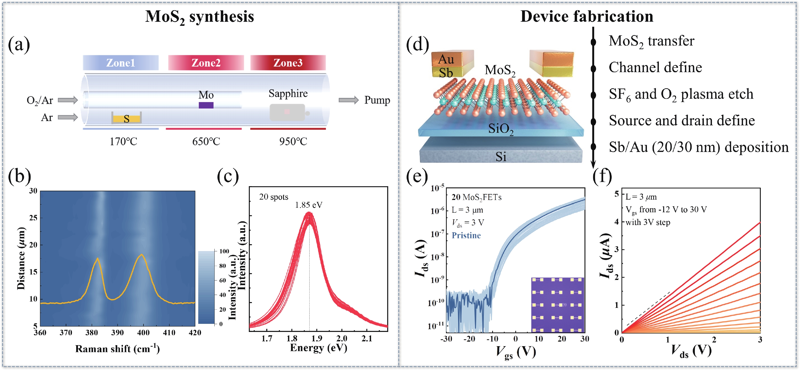
Fig. 1.  (Color online) Characterization of a CVD-grown monolayer MoS2 film. (a) Schematic presentation of the seeding-promoted CVD with a customized inner reactor for the synthesis of monolayer MoS2. (b) and (c) Line scan of Raman spectra and PL spectra of the monolayer MoS2 film, performed in this study with a 488 nm laser. (d) A schematic diagram and process flow detailing the device structure are provided. A 285 nm SiO2 layer serves as the gate dielectric in this design. (e) Transfer characteristics of 20 MoS2 FETs with L = 3 μm and W = 4 μm, under Vds = 3 V. (f) Corresponding output characteristics of the MoS2 FET. Vgs is stepped up from −12 to 30 V by increments of 3 V.

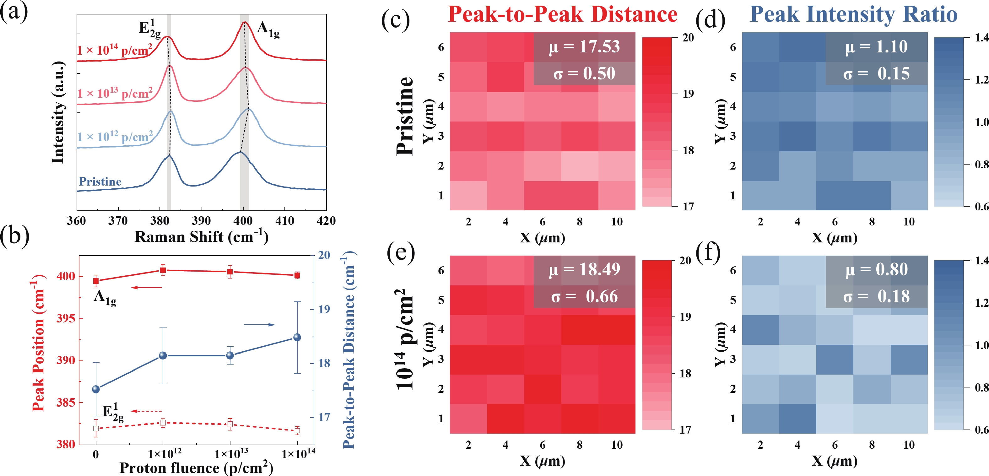
Fig. 2.  (Color online) Raman analysis of the MoS2 FETs before and after 30 keV proton irradiation. (a) Raman spectra of monolayer MoS2 analysis under different proton fluence. (b) Position of $ {\text{E}}_{\text{2g}}^{\text{1}} $ and $ {\text{A}}_{\text{1g}} $ in correlation with the proton fluence. The peak position's error bars represent the largest uncertainty present. (c) The peak-to-peak distance and (d) peak intensity ratio for the Raman spectra were measured at 30 different locations within a 5 μm by 6 μm area before irradiation. Insets in the upper right corner of the color maps show the mean (μ) and standard deviation (σ) for each parameter. (e) The peak-to-peak distance and (f) peak intensity ratio for the Raman spectra at the same points after irradiation with a fluence of 1014 p/cm2.

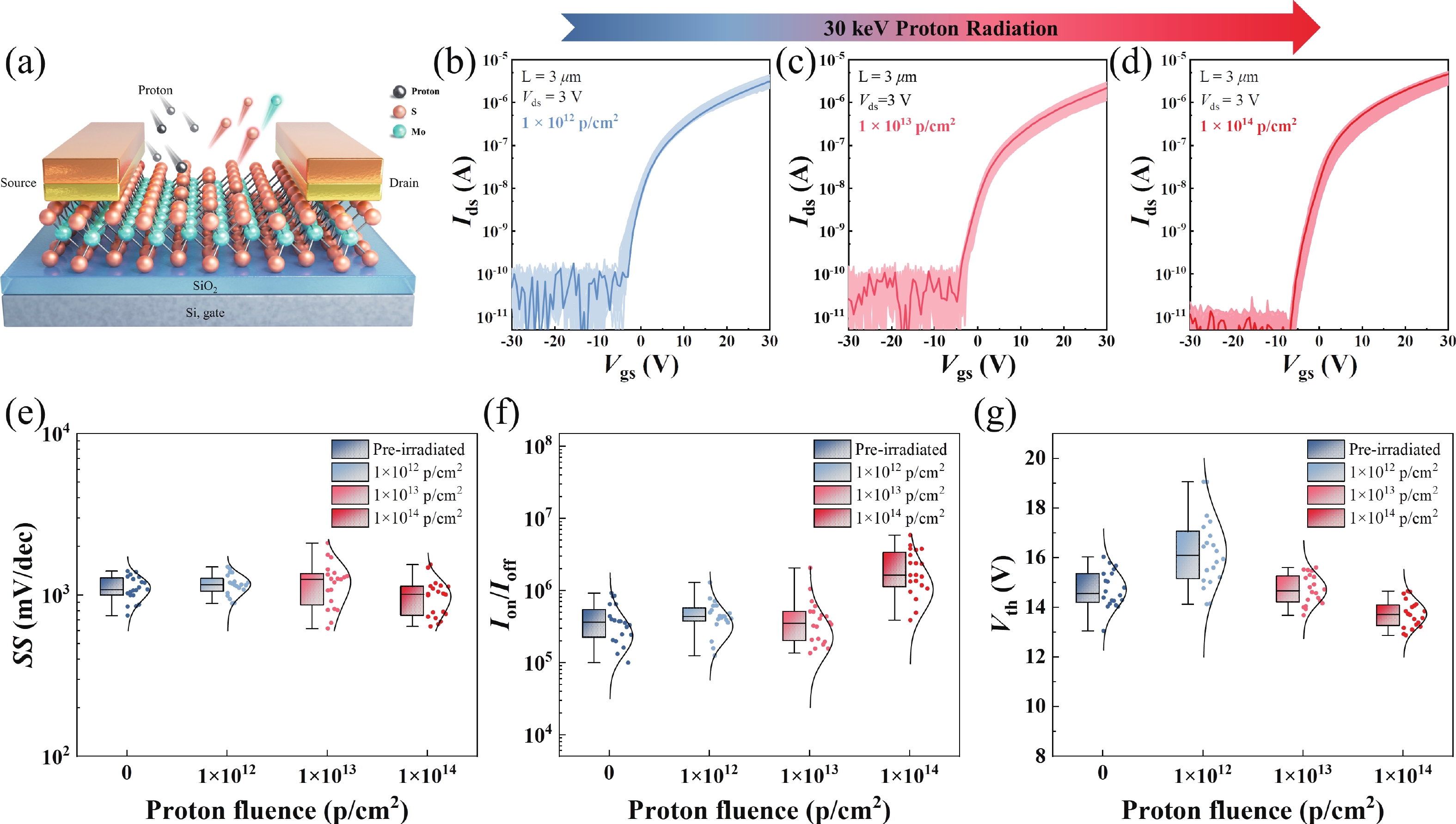
Fig. 3.  (Color online) Electrical performance of the MoS2 FETs before and after 30 keV proton irradiation. (a) A diagrammatic representation of the DD effect in the MoS2 FET caused by proton irradiation. Representative transfer characteristics obtained from 20 monolayer MoS2 FETs after proton irradiation with a total fluence of (b) 1012 p/cm2, (c) 1013 p/cm2, and (d) 1014 p/cm2. Statistical measurements of (e) SS, (f) Ion/Ioff, and (g) Vth change, with three different proton irradiation fluences of 1012, 1013, and 1014 p/cm2.

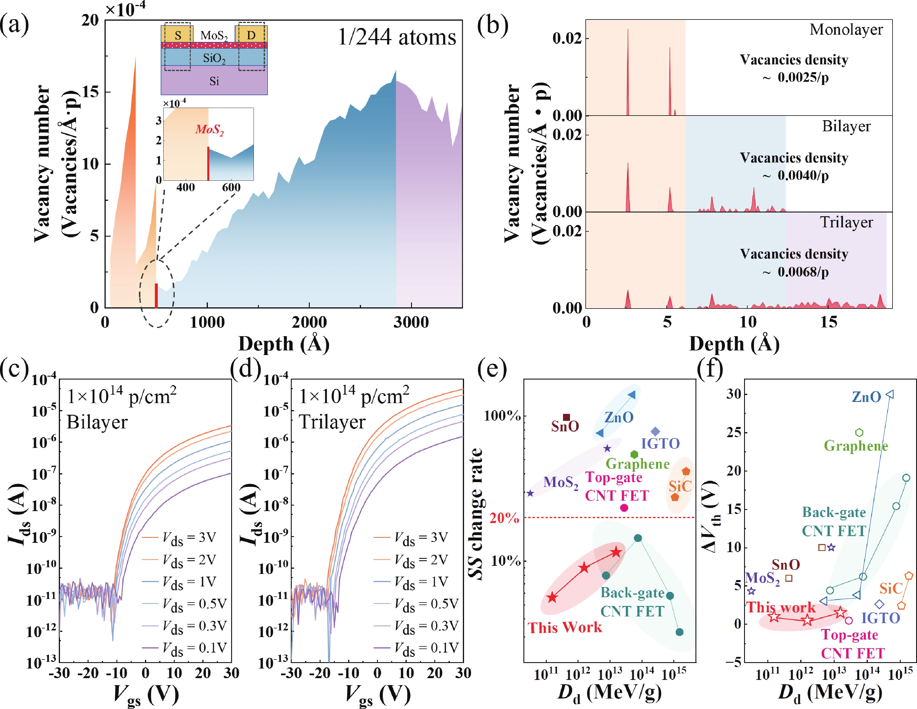
Fig. 4.  (Color online) The relationship between radiation absorption cross-section and radiation tolerance. (a) Simulation results of the vacancy number in the source/drain region (Sb/Au/MoS2/SiO2/Si) by SRIM. Inset illustrates the simulation domain, encompassing the source/drain contact region. (b) Simulation results of vacancies number in the monolayer, bilayer and trilayer by SRIM. Transfer characteristics of (c) bilayer and (d) trilayer MoS2 FETs after 1014 p/cm2 proton irradiation measured at different Vds. Benchmark of the change of (e) ΔSS and (f) ΔVth caused by DD in other radiation-hard FETs[11, 20, 21, 3539].

[1]
Zhu M G, Zhang Z, Peng L M. High-performance and radiation-hard carbon nanotube complementary static random-access memory. Adv Electron Mater, 2019, 5, 1900313 doi: 10.1002/aelm.201900313
[2]
Prinzie J, Simanjuntak F M, Leroux P, et al. Low-power electronic technologies for harsh radiation environments. Nat Electron, 2021, 4, 243 doi: 10.1038/s41928-021-00562-4
[3]
Meyyappan M, Koehne J E, Han J W. Nanoelectronics and nanosensors for space exploration. MRS Bull, 2015, 40, 822 doi: 10.1557/mrs.2015.223
[4]
Fleetwood D M. Evolution of total ionizing dose effects in MOS devices with Moore’s law scaling. IEEE Trans Nucl Sci, 2018, 65, 1465 doi: 10.1109/TNS.2017.2786140
[5]
Schranghamer T F, Pannone A, Ravichandran H, et al. Radiation resilient two-dimensional electronics. ACS Appl Mater Interfaces, 2023, 15, 26946 doi: 10.1021/acsami.3c02406
[6]
Vogl T, Sripathy K, Sharma A, et al. Radiation tolerance of two-dimensional material-based devices for space applications. Nat Commun, 2019, 10, 1202 doi: 10.5281/zenodo.2584405
[7]
Zhu M G, Lu P, Wang X, et al. Ultra-strong comprehensive radiation effect tolerance in carbon nanotube electronics. Small, 2023, 19, 2204537 doi: 10.1002/smll.202204537
[8]
Zhu M G, Xiao H S, Yan G P, et al. Radiation-hardened and repairable integrated circuits based on carbon nanotube transistors with ion gel gates. Nat Electron, 2020, 3, 622 doi: 10.1038/s41928-020-0465-1
[9]
Zhu M G, Zhou J S, Sun P K, et al. Analyzing gamma-ray irradiation effects on carbon nanotube top-gated field-effect transistors. ACS Appl Mater Interfaces, 2021, 13, 47756 doi: 10.1021/acsami.1c13651
[10]
Lu P, Zhu M G, Zhao P X, et al. Heavy ion displacement damage effect in carbon nanotube field effect transistors. ACS Appl Mater Interfaces, 2023, 15, 10936 doi: 10.1021/acsami.2c20005
[11]
Zhang X R, Zhu H P, Peng S A, et al. Radiation-hardened property of single-walled carbon nanotube film-based field-effect transistors under low-energy proton irradiation. J Semicond, 2021, 42, 112002 doi: 10.1088/1674-4926/42/11/112002
[12]
Liang C, Ma R, Li K, et al. Laser-induced single-event transients in black phosphorus MOSFETs. IEEE Trans Nucl Sci, 2019, 66, 384 doi: 10.1109/TNS.2018.2877412
[13]
Li W S, Gong X S, Yu Z H, et al. Approaching the quantum limit in two-dimensional semiconductor contacts. Nature, 2023, 613, 274 doi: 10.1038/s41586-022-05431-4
[14]
Fan D X, Li W S, Qiu H, et al. Two-dimensional semiconductor integrated circuits operating at gigahertz frequencies. Nat Electron, 2023, 6, 879 doi: 10.1038/s41928-023-01052-5
[15]
Ning H K, Yu Z H, Zhang Q T, et al. An in-memory computing architecture based on a duplex two-dimensional material structure for in situ machine learning. Nat Nanotechnol, 2023, 18, 493 doi: 10.1038/s41565-023-01343-0
[16]
Jiang J F, Xu L, Du L J, et al. Yttrium-doping-induced metallization of molybdenum disulfide for ohmic contacts in two-dimensional transistors. Nat Electron, 2024, 7, 545 doi: 10.1038/s41928-024-01176-2
[17]
Zheng S Y, Zeng Y, Chen Z J. Investigation of total-ionizing dose effects on the two-dimensional transition metal dichalcogenide field-effect transistors. IEEE Access, 2019, 7, 79989 doi: 10.1109/ACCESS.2019.2922408
[18]
Li H Y, Liu C M, Zhang Y Q, et al. Electron radiation effects on the structural and electrical properties of MoS2 field effect transistors. Nanotechnology, 2019, 30, 485201 doi: 10.1088/1361-6528/ab3ce2
[19]
Wang P, Perini C J, O’Hara A, et al. Total ionizing dose effects and proton-induced displacement damage on MoS2-interlayer-MoS2 tunneling junctions. IEEE Trans Nucl Sci, 2019, 66, 420 doi: 10.1109/TNS.2018.2879632
[20]
Kim T Y, Cho K, Park W, et al. Irradiation effects of high-energy proton beams on MoS2 field effect transistors. ACS Nano, 2014, 8, 2774 doi: 10.1021/nn4064924
[21]
Zhang Y F, Chen X F, Wang H S, et al. Electronic properties of multilayer MoS2 field effect transistor with unique irradiation resistance. J Phys Chem C, 2021, 125, 2089 doi: 10.1021/acs.jpcc.0c09666
[22]
Ochedowski O, Marinov K, Wilbs G, et al. Radiation hardness of graphene and MoS2 field effect devices against swift heavy ion irradiation. J Appl Phys, 2013, 113, 153005 doi: 10.1063/1.4808460
[23]
He Z Y, Zhao R, Chen X F, et al. Defect engineering in single-layer MoS2 using heavy ion irradiation. ACS Appl Mater Interfaces, 2018, 10, 42524 doi: 10.1021/acsami.8b17145
[24]
Madauß L, Ochedowski O, Lebius H, et al. Defect engineering of single- and few-layer MoS2 by swift heavy ion irradiation. 2D Mater, 2016, 4, 015034 doi: 10.1088/2053-1583/4/1/015034
[25]
Jun I, Xapsos M A, Messenger S R, et al. Proton nonionizing energy loss (NIEL) for device applications. IEEE Trans Nucl Sci, 2003, 50, 1924 doi: 10.1109/TNS.2003.820760
[26]
Huhtinen M. Simulation of non-ionising energy loss and defect formation in silicon. Nucl Instrum Meth Phys Res Sect A Accel Spectrometers Detect Assoc Equip, 2002, 491, 194 doi: 10.1016/S0168-9002(02)01227-5
[27]
Lu X R, Shu X Y, Wang L, et al. Heavy-ion irradiation effects on Gd2Zr2O7 ceramics bearing complex nuclear waste. J Alloys Compd, 2019, 771, 973 doi: 10.1016/j.jallcom.2018.09.006
[28]
Lee C G, Yan H G, Brus L E, et al. Anomalous lattice vibrations of single-and few-layer MoS2. ACS Nano, 2010, 4, 2695 doi: 10.1021/nn1003937
[29]
Li T T, Guo W, Ma L, et al. Epitaxial growth of wafer-scale molybdenum disulfide semiconductor single crystals on sapphire. Nat Nanotechnol, 2021, 16, 1201 doi: 10.1038/s41565-021-00963-8
[30]
Hui Y Y, Liu X F, Jie W J, et al. Exceptional tunability of band energy in a compressively strained trilayer MoS2 sheet. ACS Nano, 2013, 7, 7126 doi: 10.1021/nn4024834
[31]
Parkin W M, Balan A, Liang L B, et al. Raman shifts in electron-irradiated monolayer MoS2. ACS Nano, 2016, 10, 4134 doi: 10.1021/acsnano.5b07388
[32]
Hong J H, Hu Z X, Probert M, et al. Exploring atomic defects in molybdenum disulphide monolayers. Nat Commun, 2015, 6, 6293 doi: 10.1038/ncomms7293
[33]
Simoen E, Rafi J M, Mercha A, et al. Degradation of deep submicron partially depleted SOI CMOS transistors under MeV proton irradiation. Proceedings of the 18th Symposium on Microelectronics Technology and Devices-SBMICRO, 2003
[34]
Esposito M G, Manuel J E, Privat A, et al. Investigating heavy-ion effects on 14-nm process FinFETs: displacement damage versus total ionizing dose. IEEE Trans Nucl Sci, 2021, 68, 724 doi: 10.1109/TNS.2021.3072886
[35]
Bonaldo S, Martinella C, Race S, et al. Radiation-induced effects in SiC vertical power MOSFETs irradiated at ultrahigh doses. IEEE Trans Nucl Sci, 2024, 71, 418 doi: 10.1109/TNS.2024.3366190
[36]
Zeng J, Ma P C, Zhang S X, et al. Unrecovered ion-irradiated damage after thermal annealing in graphene field effect transistors. Appl Surf Sci, 2022, 588, 153005 doi: 10.1016/j.apsusc.2022.153005
[37]
Shin M G, Hwang S H, Cha H S, et al. Effects of proton beam irradiation on the physical and chemical properties of IGTO thin films with different thicknesses for thin-film transistor applications. Surf Interfaces, 2021, 23, 100990 doi: 10.1016/j.surfin.2021.100990
[38]
Jeong H Y, Kwon S H, Joo H J, et al. Radiation-tolerant p-type SnO thin-film transistors. IEEE Electron Device Lett, 2019, 40, 1124 doi: 10.1109/LED.2019.2914252
[39]
Park B, Ho D, Kwon G, et al. Solution-processed rad-hard amorphous metal-oxide thin-film transistors. Adv Funct Mater, 2018, 28, 1802717 doi: 10.1002/adfm.201802717
[40]
Summers G P, Burke E A, Shapiro P, et al. Damage correlations in semiconductors exposed to gamma, electron and proton radiations. IEEE Trans Nucl Sci, 1993, 40, 1372 doi: 10.1109/23.273529
[41]
Huang X N, Shi J Y, Yao Y, et al. Layer thickness influenced irradiation effects of proton beam on MoS2 field effect transistors. Nanotechnology, 2021, 32, 135204 doi: 10.1088/1361-6528/abd129
[42]
Srour J R, Palko J W. Displacement damage effects in irradiated semiconductor devices. IEEE Trans Nucl Sci, 2013, 60, 1740 doi: 10.1109/TNS.2013.2261316

24090027Supporting_Information.pdf

  • Search

    Advanced Search >>

    GET CITATION

    shu

    Export: BibTex EndNote

    Article Metrics

    Article views: 487 Times PDF downloads: 52 Times Cited by: 0 Times

    History

    Received: 15 September 2024 Revised: 25 October 2024 Online: Accepted Manuscript: 14 November 2024Uncorrected proof: 20 November 2024Published: 15 December 2024

    Catalog

      Email This Article

      User name:
      Email:*请输入正确邮箱
      Code:*验证码错误
      Kaiyue He, Zhanqi Li, Taotao Li, Yifu Sun, Shitong Zhu, Chao Wu, Huiping Zhu, Peng Lu, Xinran Wang, Maguang Zhu. Displacement damage effects in MoS2-based electronics[J]. Journal of Semiconductors, 2024, 45(12): 122701. doi: 10.1088/1674-4926/24090027 ****K Y He, Z Q Li, T T Li, Y F Sun, S T Zhu, C Wu, H P Zhu, P Lu, X R Wang, and M G Zhu, Displacement damage effects in MoS2-based electronics[J]. J. Semicond., 2024, 45(12), 122701 doi: 10.1088/1674-4926/24090027
      Citation:
      Kaiyue He, Zhanqi Li, Taotao Li, Yifu Sun, Shitong Zhu, Chao Wu, Huiping Zhu, Peng Lu, Xinran Wang, Maguang Zhu. Displacement damage effects in MoS2-based electronics[J]. Journal of Semiconductors, 2024, 45(12): 122701. doi: 10.1088/1674-4926/24090027 ****
      K Y He, Z Q Li, T T Li, Y F Sun, S T Zhu, C Wu, H P Zhu, P Lu, X R Wang, and M G Zhu, Displacement damage effects in MoS2-based electronics[J]. J. Semicond., 2024, 45(12), 122701 doi: 10.1088/1674-4926/24090027

      Displacement damage effects in MoS2-based electronics

      DOI: 10.1088/1674-4926/24090027
      More Information
      • Kaiyue He, a Ph.D. student at School of Integrated Circuits, Nanjing University, under the supervision of Prof. Xinran wang and Prof. Maguang Zhu. Her research focuses on radiation-hard MoS2 integrated circuits
      • Zhanqi Li, a Master’s student at School of Integrated Circuits, Nanjing University, under the supervision of Prof. Maguang Zhu. His research focuses on simulation of radiation effects
      • Maguang Zhu, an Assistant professor at School of Integrated Circuits, Nanjing University. He received his Ph.D. degree in Physical Electronics from Peking University in 2020. He was a postdoctoral researcher in Peking University from 2021 to 2022. He focuses on the high performance and radiation-hard carbon nanotube integrated circuits
      • Corresponding author: mgzhu@nju.edu.cn
      • Received Date: 2024-09-15
      • Revised Date: 2024-10-25
      • Available Online: 2024-11-14

      Catalog

        /

        DownLoad:  Full-Size Img  PowerPoint
        Return
        Return