J. Semicond. > 2025, Volume 46 > Issue 4 > 042102

SPECIAL TOPIC ARTICLES

Layer-dependent optical and dielectric properties of CdSe semiconductor colloidal quantum wells characterized by spectroscopic ellipsometry

Chenlin Wang1, Haixiao Zhao2, Xian Zhao2, 3, Baoqing Sun1, 2, Jie Lian1, 2 and Yuan Gao1, 2,

+ Author Affiliations

 Corresponding author: Yuan Gao, yuan.gao@sdu.edu.cn

DOI: 10.1088/1674-4926/24100011CSTR: 32376.14.1674-4926.24100011

PDF

Turn off MathJax

Abstract: Semiconductor colloidal quantum wells (CQWs) with atomic-precision layer thickness are rapidly gaining attention for next-generation optoelectronic applications due to their tunable optical and electronic properties. In this study, we investigate the dielectric and optical characteristics of CdSe CQWs with monolayer numbers ranging from 2 to 7, synthesized via thermal injection and atomic layer (c-ALD) deposition techniques. Through a combination of spectroscopic ellipsometry (SE) and first-principles calculations, we demonstrate the significant tunability of the bandgap, refractive index, and extinction coefficient, driven by quantum confinement effects. Our results show a decrease in bandgap from 3.1 to 2.0 eV as the layer thickness increases. Furthermore, by employing a detailed analysis of the absorption spectra, accounting for exciton localization and asymmetric broadening, we precisely capture the relationship between monolayer number and exciton binding energy. These findings offer crucial insights for optimizing CdSe CQWs in optoelectronic device design by leveraging their layer-dependent properties.

Key words: CdSe CQWsbandgapspectroscopic ellipsometrymonolayer numberexciton binding energy


[1]
Diroll B T, Guzelturk B, Po H, et al. 2D Ⅱ–Ⅵ semiconductor nanoplatelets: From material synthesis to optoelectronic integration. Chem Rev, 2023, 123, 3543 doi: 10.1021/acs.chemrev.2c00436
[2]
Macias-Pinilla D F, Planelles J, Mora-Seró I, et al. Comparison between trion and exciton electronic properties in CdSe and PbS nanoplatelets. J Phys Chem C, 2021, 125, 15614 doi: 10.1021/acs.jpcc.1c03880
[3]
Scott R, Heckmann J, Prudnikau A V, et al. Directed emission of CdSe nanoplatelets originating from strongly anisotropic 2D electronic structure. Nat Nanotechnol, 2017, 12, 1155 doi: 10.1038/nnano.2017.177
[4]
Tanghe I, Samoli M, Wagner I, et al. Optical gain and lasing from bulk cadmium sulfide nanocrystals through bandgap renormalization. Nat Nanotechnol, 2023, 18, 1423 doi: 10.1038/s41565-023-01521-0
[5]
Zhang Z T, Thung Y T, Chen X X, et al. Study of complex optical constants of neat cadmium selenide nanoplatelets thin films by spectroscopic ellipsometry. J Phys Chem Lett, 2021, 12, 191 doi: 10.1021/acs.jpclett.0c03304
[6]
Diroll B T, Schaller R D. Reexamination of the giant oscillator strength effect in CdSe nanoplatelets. J Phys Chem C, 2023, 127, 4601 doi: 10.1021/acs.jpcc.2c08079
[7]
Ibrahem M A, Waris M, Miah M R, et al. Orientation-dependent photoconductivity of quasi-2D nanocrystal self-assemblies: Face-down, edge-up versus randomly oriented quantum wells. Small, 2024, 20, 2401423 doi: 10.1002/smll.202401423
[8]
Das S, Tripathi A, Parida A, et al. Visible light photodetectors based on hydrothermally synthesized Cd-Se-Te nanostructures. ACS Appl Electron Mater, 2024, 6, 6522 doi: 10.1021/acsaelm.4c01000
[9]
Zhang Y, Xiang W B, Wang R, et al. Study of the mechanisms of the phonon bottleneck effect in CdSe/CdS core/shell quantum dots and nanoplatelets and their application in hot carrier multi-junction solar cells. Nanoscale Adv, 2023, 5, 5594 doi: 10.1039/D3NA00557G
[10]
Liao S X, Yang Z Z, Lin J D, et al. A hierarchical structure perovskite quantum dots film for laser-driven projection display. Adv Funct Mater, 2023, 33, 2210558 doi: 10.1002/adfm.202210558
[11]
Kim J, Roh J, Park M, et al. Recent advances and challenges of colloidal quantum dot light-emitting diodes for display applications. Adv Mater, 2024, 36, 2212220 doi: 10.1002/adma.202212220
[12]
Park K D, May M A, Leng H X, et al. Tip-enhanced strong coupling spectroscopy, imaging, and control of a single quantum emitter. Sci Adv, 2019, 5, eaav5931 doi: 10.1126/sciadv.aav5931
[13]
Jo K, Marino E, Lynch J, et al. Direct nano-imaging of light-matter interactions in nanoscale excitonic emitters. Nat Commun, 2023, 14, 2649 doi: 10.1038/s41467-023-38189-y
[14]
Ugur E, Said A A, Dally P, et al. Enhanced cation interaction in perovskites for efficient tandem solar cells with silicon. Science, 2024, 385, 533 doi: 10.1126/science.adp1621
[15]
Kumar D, Li H R, Das U K, et al. Flexible solution-processable black-phosphorus-based optoelectronic memristive synapses for neuromorphic computing and artificial visual perception applications. Adv Mater, 2023, 35, 2300446 doi: 10.1002/adma.202300446
[16]
Rani A, Verma A, Yadav B C. Advancements in transition metal dichalcogenides (TMDCs) for self-powered photodetectors: Challenges, properties, and functionalization strategies. Mater Adv, 2024, 5, 3535 doi: 10.1039/D3MA01152F
[17]
Yao Y G, Zhu Y K, Hu A, et al. Temperature-regulated in-plane exciton dynamics in CdSe/CdSeS colloidal quantum well heterostructures. ACS Photonics, 2023, 10, 4052 doi: 10.1021/acsphotonics.3c01123
[18]
Marder A A, Cassidy J, Harankahage D, et al. CdS/CdSe/CdS spherical quantum wells with near-unity biexciton quantum yield for light-emitting-device applications. ACS Materials Lett, 2023, 5, 1411 doi: 10.1021/acsmaterialslett.3c00110
[19]
Ba G H, Yang Y M, Huang F, et al. Gradient alloy shell enabling colloidal quantum wells light-emitting diodes with efficiency exceeding 22%. Nano Lett, 2024, 24, 4454 doi: 10.1021/acs.nanolett.4c00276
[20]
Taghipour N, Delikanli S, Shendre S, et al. Sub-single exciton optical gain threshold in colloidal semiconductor quantum wells with gradient alloy shelling. Nat Commun, 2020, 11, 3305 doi: 10.1038/s41467-020-17032-8
[21]
Delikanli S, Yu G N, Yeltik A, et al. Ultrathin highly luminescent two-monolayer colloidal CdSe nanoplatelets. Adv Funct Mater, 2019, 29, 1901028 doi: 10.1002/adfm.201901028
[22]
Jana S, Martins R, Fortunato E. Stacking-dependent electrical transport in a colloidal CdSe nanoplatelet thin-film transistor. Nano Lett, 2022, 22, 2780 doi: 10.1021/acs.nanolett.1c04822
[23]
Sharma A, Sharma M, Gungor K, et al. Near-infrared-emitting five-monolayer thick copper-doped CdSe nanoplatelets. Adv Optical Mater, 2019, 7, 1900831 doi: 10.1002/adom.201900831
[24]
Khan A H, Pinchetti V, Tanghe I, et al. Tunable and efficient red to near-infrared photoluminescence by synergistic exploitation of core and surface silver doping of CdSe nanoplatelets. Chem Mater, 2019, 31, 1450 doi: 10.1021/acs.chemmater.8b05334
[25]
Kormilina T K, Cherevkov S A, Fedorov A V, et al. Cadmium chalcogenide nano-heteroplatelets: Creating advanced nanostructured materials by shell growth, substitution, and attachment. Small, 2017, 13, 1702300 doi: 10.1002/smll.201702300
[26]
Li Y L, Wang L F, Xiang D M, et al. Dielectric and wavefunction engineering of electron spin lifetime in colloidal nanoplatelet heterostructures. Adv Sci, 2024, 11, 2306518 doi: 10.1002/advs.202306518
[27]
Altintas Y, Gungor K, Gao Y, et al. Giant alloyed hot injection shells enable ultralow optical gain threshold in colloidal quantum wells. ACS Nano, 2019, 13, 10662 doi: 10.1021/acsnano.9b04967
[28]
Christodoulou S, Climente J I, Planelles J, et al. Chloride-induced thickness control in CdSe nanoplatelets. Nano Lett, 2018, 18, 6248 doi: 10.1021/acs.nanolett.8b02361
[29]
Diroll B T. Colloidal quantum wells for optoelectronic devices. J Mater Chem C, 2020, 8, 10628 doi: 10.1039/D0TC01164A
[30]
Ashry M, Fares S. Radiation effect on the optical and electrical properties of CdSe(In)/p-Si heterojunction photovoltaic solar cells. J Semicond, 2012, 33, 102001 doi: 10.1088/1674-4926/33/10/102001
[31]
Bao Y T, Wang X R, Xu S J. Sub-bandgap refractive indexes and optical properties of Si-doped β-Ga2O3 semiconductor thin films. J Semicond, 2022, 43, 062802 doi: 10.1088/1674-4926/43/6/062802
[32]
She C X, Fedin I, Dolzhnikov D S, et al. Low-threshold stimulated emission using colloidal quantum wells. Nano Lett, 2014, 14, 2772 doi: 10.1021/nl500775p
[33]
Gao Y, Li M J, Delikanli S, et al. Low-threshold lasing from colloidal CdSe/CdSeTe core/alloyed-crown type-II heteronanoplatelets. Nanoscale, 2018, 10, 9466 doi: 10.1039/C8NR01838C
[34]
Galle T, Spittel D, Weiß N, et al. Simultaneous ligand and cation exchange of colloidal CdSe nanoplatelets toward PbSe nanoplatelets for application in photodetectors. J Phys Chem Lett, 2021, 12, 5214 doi: 10.1021/acs.jpclett.1c01362
[35]
Diroll B T, Schaller R D. Intersubband relaxation in CdSe colloidal quantum wells. ACS Nano, 2020, 14, 12082 doi: 10.1021/acsnano.0c05459
[36]
Li Y L. Measurement of the optical dielectric function of monolayer transition metal dichalcogenides: MoS2, MoSe2, WS2, and WSe2. Phys Rev B, 2014, 90, 205422 doi: 10.1103/PhysRevB.90.205422
[37]
Morozov Y V, Kuno M. Optical constants and dynamic conductivities of single layer MoS2, MoSe2, and WSe2. Appl Phys Lett, 2015, 107, 083103 doi: 10.1063/1.4929700
[38]
Hu D B, Yang X X, Li C, et al. Probing optical anisotropy of nanometer-thin van der waals microcrystals by near-field imaging. Nat Commun, 2017, 8, 1471 doi: 10.1038/s41467-017-01580-7
[39]
Chen X Z, Hu D B, Mescall R, et al. Modern scattering-type scanning near-field optical microscopy for advanced material research. Adv Mater, 2019, 31, 1804774 doi: 10.1002/adma.201804774
[40]
Wang C L, Ying M J, Lian J, et al. Structural, optical and dielectric properties of (Co and Sm) co-implanting O-polar ZnO films on sapphire substrate. J Alloys Compd, 2021, 876, 160017 doi: 10.1016/j.jallcom.2021.160017
[41]
Wang C L, Ying M J, Lian J, et al. Structural, optical and half-metallic properties of Mn and As co-implanted ZnO thin films. Appl Surf Sci, 2022, 575, 151703 doi: 10.1016/j.apsusc.2021.151703
[42]
Ye C Y, Lin W, Zhou J, et al. Optical properties of InN studied by spectroscopic ellipsometry. J Semicond, 2016, 37, 102002 doi: 10.1088/1674-4926/37/10/102002
[43]
Wei M Y, Lian J, Zhang Y, et al. Layer-dependent optical and dielectric properties of centimeter-scale PdSe2 films grown by chemical vapor deposition. NPJ 2D Mater Appl, 2022, 6, 1 doi: 10.1038/s41699-021-00282-5
[44]
Gu H G, Song B K, Fang M S, et al. Layer-dependent dielectric and optical properties of centimeter-scale 2D WSe2: Evolution from a single layer to few layers. Nanoscale, 2019, 11, 22762 doi: 10.1039/C9NR04270A
[45]
Zhao M L, Shi Y J, Dai J, et al. Ellipsometric study of the complex optical constants of a CsPbBr3 perovskite thin film. J Mater Chem C, 2018, 6, 10450 doi: 10.1039/C8TC03222J
[46]
Ströhl F, Wolfson D L, Opstad I S, et al. Label-free superior contrast with c-band ultra-violet extinction microscopy. Light Sci Appl, 2023, 12, 56 doi: 10.1038/s41377-023-01105-6
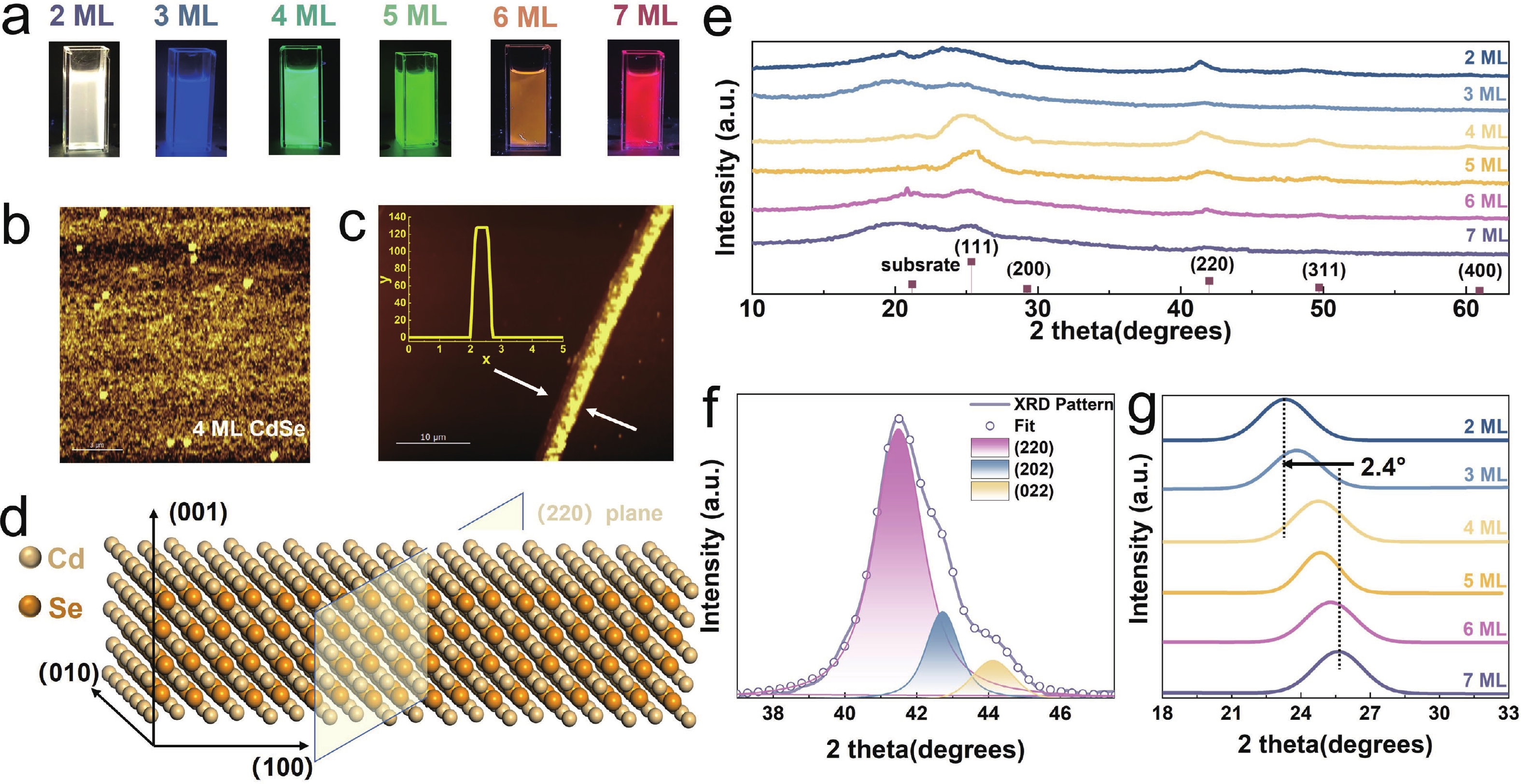
Fig. 1.  (Color online) (a) Photographs of 2 to 7 ML CdSe CQWs under ultraviolet light, showing the variation in photoluminescence with increasing layer thickness. (b) AFM surface topography of a 4 ML CdSe CQW film on a quartz substrate, illustrating the smoothness of the film. Scale bar: 3 μm. (c) Scratch height profile of the 4 ML CdSe CQW film, showing the step height between the film and the substrate. (d) Visualization of the (220) crystal plane in the CdSe CQW model. (e) Static X-ray diffraction (XRD) patterns of 2 to 7 ML CdSe CQWs, indicating structural properties and phase purity. (f) Gaussian fitting of the (220) plane in the 4 ML CdSe CQWs. (g) Enlarged view of the (111) diffraction peaks for 2 to 7 ML CdSe CQWs.

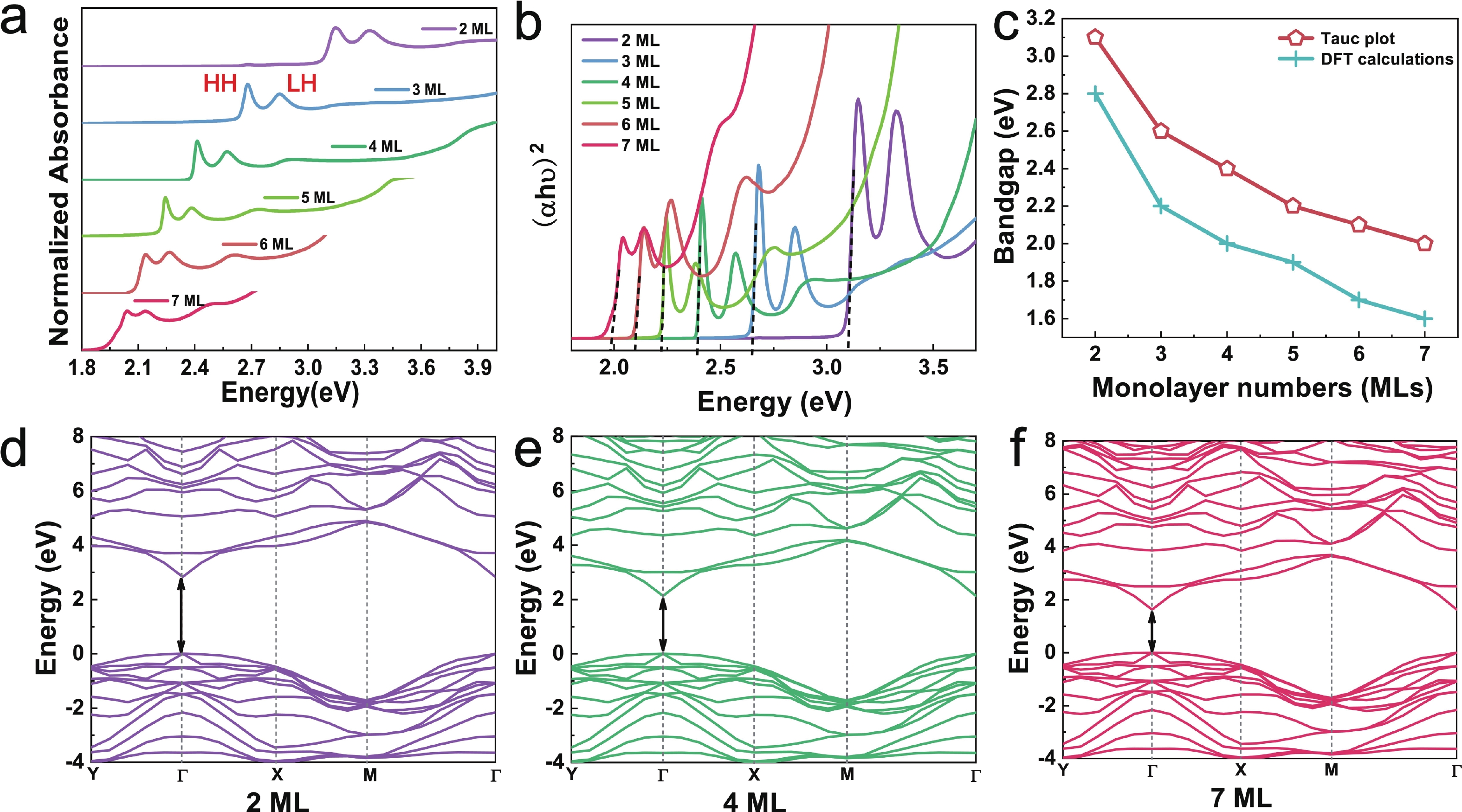
Fig. 2.  (Color online) (a) Absorption spectra of 2 to 7 ML CdSe CQWs, illustrating the layer-dependent shift in absorption peaks. HH and LH represent the heavy-hole and light-hole transitions in the absorption spectra. (b) Tauc plots for 2 to 7 ML CdSe CQWs, with dotted lines indicating the intercept method used to estimate the optical bandgap. (c) Relationship between the optical bandgap as derived from the Tauc plots (red line) and density functional theory (DFT) calculations (blue line) as a function of monolayer thickness. Simulated band structure obtained through first-principles calculations for (d) 2 ML CdSe CQWs, (e) 4 ML CdSe CQWs, and (f) 7 ML CdSe CQWs, highlighting the changes in electronic structure with increasing monolayers.

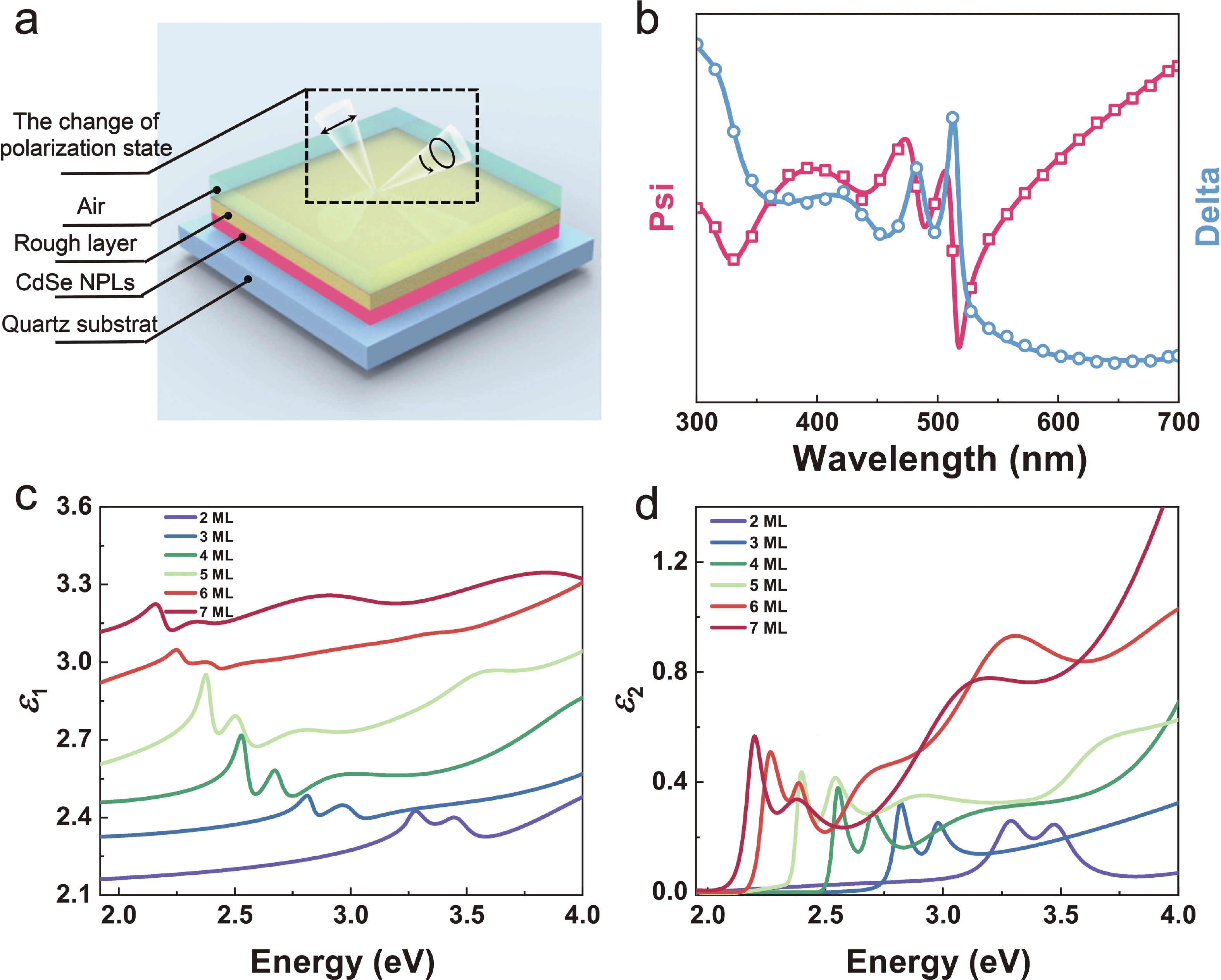
Fig. 3.  (Color online) (a) Structural model of the CdSe CQW film on a quartz substrate. (b) Experimental spectroscopic ellipsometry spectra (solid lines) and best-fit curves (dots) for 4 ML CdSe CQWs at a 65° incidence angle. (c) Real part of the dielectric function for 2 to 7 ML CdSe CQWs, showing the variation with increasing monolayer thickness. (d) Imaginary part of the dielectric function for 2 to 7 ML CdSe CQWs, illustrating the evolution of optical transitions with layer thickness.

Fig. 4.  (Color online) (a) Refractive index and (b) extinction coefficient of 2 to 7 ML CdSe CQW films, demonstrating their layer-dependent optical properties. HH and LH represent the two prominent absorption peaks of CdSe CQW films. (c) Variation of the refractive index peak values from (a) with monolayer numbers. The inset illustrates the change in extinction coefficient peak values from (b) with monolayer numbers. (d) Variation of the normalized refractive index and normalized extinction coefficient (the inset) with monolayer number. (e) (Top) Deconvolution of the absorption spectrum for 4 ML CdSe CQWs, showing contributions from light-hole (LH) and heavy-hole (HH) excitons as well as free carriers. The exciton binding energy, estimated as 171 meV, is indicated. (Bottom) Absorption coefficient of 4 ML CdSe CQWs, with the positions of the LH and HH exciton lines highlighted. (f) Relationship between exciton binding energy and optical bandgap as a function of monolayer thickness in CdSe CQWs.

[1]
Diroll B T, Guzelturk B, Po H, et al. 2D Ⅱ–Ⅵ semiconductor nanoplatelets: From material synthesis to optoelectronic integration. Chem Rev, 2023, 123, 3543 doi: 10.1021/acs.chemrev.2c00436
[2]
Macias-Pinilla D F, Planelles J, Mora-Seró I, et al. Comparison between trion and exciton electronic properties in CdSe and PbS nanoplatelets. J Phys Chem C, 2021, 125, 15614 doi: 10.1021/acs.jpcc.1c03880
[3]
Scott R, Heckmann J, Prudnikau A V, et al. Directed emission of CdSe nanoplatelets originating from strongly anisotropic 2D electronic structure. Nat Nanotechnol, 2017, 12, 1155 doi: 10.1038/nnano.2017.177
[4]
Tanghe I, Samoli M, Wagner I, et al. Optical gain and lasing from bulk cadmium sulfide nanocrystals through bandgap renormalization. Nat Nanotechnol, 2023, 18, 1423 doi: 10.1038/s41565-023-01521-0
[5]
Zhang Z T, Thung Y T, Chen X X, et al. Study of complex optical constants of neat cadmium selenide nanoplatelets thin films by spectroscopic ellipsometry. J Phys Chem Lett, 2021, 12, 191 doi: 10.1021/acs.jpclett.0c03304
[6]
Diroll B T, Schaller R D. Reexamination of the giant oscillator strength effect in CdSe nanoplatelets. J Phys Chem C, 2023, 127, 4601 doi: 10.1021/acs.jpcc.2c08079
[7]
Ibrahem M A, Waris M, Miah M R, et al. Orientation-dependent photoconductivity of quasi-2D nanocrystal self-assemblies: Face-down, edge-up versus randomly oriented quantum wells. Small, 2024, 20, 2401423 doi: 10.1002/smll.202401423
[8]
Das S, Tripathi A, Parida A, et al. Visible light photodetectors based on hydrothermally synthesized Cd-Se-Te nanostructures. ACS Appl Electron Mater, 2024, 6, 6522 doi: 10.1021/acsaelm.4c01000
[9]
Zhang Y, Xiang W B, Wang R, et al. Study of the mechanisms of the phonon bottleneck effect in CdSe/CdS core/shell quantum dots and nanoplatelets and their application in hot carrier multi-junction solar cells. Nanoscale Adv, 2023, 5, 5594 doi: 10.1039/D3NA00557G
[10]
Liao S X, Yang Z Z, Lin J D, et al. A hierarchical structure perovskite quantum dots film for laser-driven projection display. Adv Funct Mater, 2023, 33, 2210558 doi: 10.1002/adfm.202210558
[11]
Kim J, Roh J, Park M, et al. Recent advances and challenges of colloidal quantum dot light-emitting diodes for display applications. Adv Mater, 2024, 36, 2212220 doi: 10.1002/adma.202212220
[12]
Park K D, May M A, Leng H X, et al. Tip-enhanced strong coupling spectroscopy, imaging, and control of a single quantum emitter. Sci Adv, 2019, 5, eaav5931 doi: 10.1126/sciadv.aav5931
[13]
Jo K, Marino E, Lynch J, et al. Direct nano-imaging of light-matter interactions in nanoscale excitonic emitters. Nat Commun, 2023, 14, 2649 doi: 10.1038/s41467-023-38189-y
[14]
Ugur E, Said A A, Dally P, et al. Enhanced cation interaction in perovskites for efficient tandem solar cells with silicon. Science, 2024, 385, 533 doi: 10.1126/science.adp1621
[15]
Kumar D, Li H R, Das U K, et al. Flexible solution-processable black-phosphorus-based optoelectronic memristive synapses for neuromorphic computing and artificial visual perception applications. Adv Mater, 2023, 35, 2300446 doi: 10.1002/adma.202300446
[16]
Rani A, Verma A, Yadav B C. Advancements in transition metal dichalcogenides (TMDCs) for self-powered photodetectors: Challenges, properties, and functionalization strategies. Mater Adv, 2024, 5, 3535 doi: 10.1039/D3MA01152F
[17]
Yao Y G, Zhu Y K, Hu A, et al. Temperature-regulated in-plane exciton dynamics in CdSe/CdSeS colloidal quantum well heterostructures. ACS Photonics, 2023, 10, 4052 doi: 10.1021/acsphotonics.3c01123
[18]
Marder A A, Cassidy J, Harankahage D, et al. CdS/CdSe/CdS spherical quantum wells with near-unity biexciton quantum yield for light-emitting-device applications. ACS Materials Lett, 2023, 5, 1411 doi: 10.1021/acsmaterialslett.3c00110
[19]
Ba G H, Yang Y M, Huang F, et al. Gradient alloy shell enabling colloidal quantum wells light-emitting diodes with efficiency exceeding 22%. Nano Lett, 2024, 24, 4454 doi: 10.1021/acs.nanolett.4c00276
[20]
Taghipour N, Delikanli S, Shendre S, et al. Sub-single exciton optical gain threshold in colloidal semiconductor quantum wells with gradient alloy shelling. Nat Commun, 2020, 11, 3305 doi: 10.1038/s41467-020-17032-8
[21]
Delikanli S, Yu G N, Yeltik A, et al. Ultrathin highly luminescent two-monolayer colloidal CdSe nanoplatelets. Adv Funct Mater, 2019, 29, 1901028 doi: 10.1002/adfm.201901028
[22]
Jana S, Martins R, Fortunato E. Stacking-dependent electrical transport in a colloidal CdSe nanoplatelet thin-film transistor. Nano Lett, 2022, 22, 2780 doi: 10.1021/acs.nanolett.1c04822
[23]
Sharma A, Sharma M, Gungor K, et al. Near-infrared-emitting five-monolayer thick copper-doped CdSe nanoplatelets. Adv Optical Mater, 2019, 7, 1900831 doi: 10.1002/adom.201900831
[24]
Khan A H, Pinchetti V, Tanghe I, et al. Tunable and efficient red to near-infrared photoluminescence by synergistic exploitation of core and surface silver doping of CdSe nanoplatelets. Chem Mater, 2019, 31, 1450 doi: 10.1021/acs.chemmater.8b05334
[25]
Kormilina T K, Cherevkov S A, Fedorov A V, et al. Cadmium chalcogenide nano-heteroplatelets: Creating advanced nanostructured materials by shell growth, substitution, and attachment. Small, 2017, 13, 1702300 doi: 10.1002/smll.201702300
[26]
Li Y L, Wang L F, Xiang D M, et al. Dielectric and wavefunction engineering of electron spin lifetime in colloidal nanoplatelet heterostructures. Adv Sci, 2024, 11, 2306518 doi: 10.1002/advs.202306518
[27]
Altintas Y, Gungor K, Gao Y, et al. Giant alloyed hot injection shells enable ultralow optical gain threshold in colloidal quantum wells. ACS Nano, 2019, 13, 10662 doi: 10.1021/acsnano.9b04967
[28]
Christodoulou S, Climente J I, Planelles J, et al. Chloride-induced thickness control in CdSe nanoplatelets. Nano Lett, 2018, 18, 6248 doi: 10.1021/acs.nanolett.8b02361
[29]
Diroll B T. Colloidal quantum wells for optoelectronic devices. J Mater Chem C, 2020, 8, 10628 doi: 10.1039/D0TC01164A
[30]
Ashry M, Fares S. Radiation effect on the optical and electrical properties of CdSe(In)/p-Si heterojunction photovoltaic solar cells. J Semicond, 2012, 33, 102001 doi: 10.1088/1674-4926/33/10/102001
[31]
Bao Y T, Wang X R, Xu S J. Sub-bandgap refractive indexes and optical properties of Si-doped β-Ga2O3 semiconductor thin films. J Semicond, 2022, 43, 062802 doi: 10.1088/1674-4926/43/6/062802
[32]
She C X, Fedin I, Dolzhnikov D S, et al. Low-threshold stimulated emission using colloidal quantum wells. Nano Lett, 2014, 14, 2772 doi: 10.1021/nl500775p
[33]
Gao Y, Li M J, Delikanli S, et al. Low-threshold lasing from colloidal CdSe/CdSeTe core/alloyed-crown type-II heteronanoplatelets. Nanoscale, 2018, 10, 9466 doi: 10.1039/C8NR01838C
[34]
Galle T, Spittel D, Weiß N, et al. Simultaneous ligand and cation exchange of colloidal CdSe nanoplatelets toward PbSe nanoplatelets for application in photodetectors. J Phys Chem Lett, 2021, 12, 5214 doi: 10.1021/acs.jpclett.1c01362
[35]
Diroll B T, Schaller R D. Intersubband relaxation in CdSe colloidal quantum wells. ACS Nano, 2020, 14, 12082 doi: 10.1021/acsnano.0c05459
[36]
Li Y L. Measurement of the optical dielectric function of monolayer transition metal dichalcogenides: MoS2, MoSe2, WS2, and WSe2. Phys Rev B, 2014, 90, 205422 doi: 10.1103/PhysRevB.90.205422
[37]
Morozov Y V, Kuno M. Optical constants and dynamic conductivities of single layer MoS2, MoSe2, and WSe2. Appl Phys Lett, 2015, 107, 083103 doi: 10.1063/1.4929700
[38]
Hu D B, Yang X X, Li C, et al. Probing optical anisotropy of nanometer-thin van der waals microcrystals by near-field imaging. Nat Commun, 2017, 8, 1471 doi: 10.1038/s41467-017-01580-7
[39]
Chen X Z, Hu D B, Mescall R, et al. Modern scattering-type scanning near-field optical microscopy for advanced material research. Adv Mater, 2019, 31, 1804774 doi: 10.1002/adma.201804774
[40]
Wang C L, Ying M J, Lian J, et al. Structural, optical and dielectric properties of (Co and Sm) co-implanting O-polar ZnO films on sapphire substrate. J Alloys Compd, 2021, 876, 160017 doi: 10.1016/j.jallcom.2021.160017
[41]
Wang C L, Ying M J, Lian J, et al. Structural, optical and half-metallic properties of Mn and As co-implanted ZnO thin films. Appl Surf Sci, 2022, 575, 151703 doi: 10.1016/j.apsusc.2021.151703
[42]
Ye C Y, Lin W, Zhou J, et al. Optical properties of InN studied by spectroscopic ellipsometry. J Semicond, 2016, 37, 102002 doi: 10.1088/1674-4926/37/10/102002
[43]
Wei M Y, Lian J, Zhang Y, et al. Layer-dependent optical and dielectric properties of centimeter-scale PdSe2 films grown by chemical vapor deposition. NPJ 2D Mater Appl, 2022, 6, 1 doi: 10.1038/s41699-021-00282-5
[44]
Gu H G, Song B K, Fang M S, et al. Layer-dependent dielectric and optical properties of centimeter-scale 2D WSe2: Evolution from a single layer to few layers. Nanoscale, 2019, 11, 22762 doi: 10.1039/C9NR04270A
[45]
Zhao M L, Shi Y J, Dai J, et al. Ellipsometric study of the complex optical constants of a CsPbBr3 perovskite thin film. J Mater Chem C, 2018, 6, 10450 doi: 10.1039/C8TC03222J
[46]
Ströhl F, Wolfson D L, Opstad I S, et al. Label-free superior contrast with c-band ultra-violet extinction microscopy. Light Sci Appl, 2023, 12, 56 doi: 10.1038/s41377-023-01105-6

24100011Supplementary_Material.pdf

  • Search

    Advanced Search >>

    GET CITATION

    shu

    Export: BibTex EndNote

    Article Metrics

    Article views: 498 Times PDF downloads: 48 Times Cited by: 0 Times

    History

    Received: 10 October 2024 Revised: 08 November 2024 Online: Accepted Manuscript: 09 December 2024Uncorrected proof: 26 February 2025Published: 10 April 2025

    Catalog

      Email This Article

      User name:
      Email:*请输入正确邮箱
      Code:*验证码错误
      Chenlin Wang, Haixiao Zhao, Xian Zhao, Baoqing Sun, Jie Lian, Yuan Gao. Layer-dependent optical and dielectric properties of CdSe semiconductor colloidal quantum wells characterized by spectroscopic ellipsometry[J]. Journal of Semiconductors, 2025, 46(4): 042102. doi: 10.1088/1674-4926/24100011 ****C L Wang, H X Zhao, X Zhao, B Q Sun, J Lian, and Y Gao, Layer-dependent optical and dielectric properties of CdSe semiconductor colloidal quantum wells characterized by spectroscopic ellipsometry[J]. J. Semicond., 2025, 46(4), 042102 doi: 10.1088/1674-4926/24100011
      Citation:
      Chenlin Wang, Haixiao Zhao, Xian Zhao, Baoqing Sun, Jie Lian, Yuan Gao. Layer-dependent optical and dielectric properties of CdSe semiconductor colloidal quantum wells characterized by spectroscopic ellipsometry[J]. Journal of Semiconductors, 2025, 46(4): 042102. doi: 10.1088/1674-4926/24100011 ****
      C L Wang, H X Zhao, X Zhao, B Q Sun, J Lian, and Y Gao, Layer-dependent optical and dielectric properties of CdSe semiconductor colloidal quantum wells characterized by spectroscopic ellipsometry[J]. J. Semicond., 2025, 46(4), 042102 doi: 10.1088/1674-4926/24100011

      Layer-dependent optical and dielectric properties of CdSe semiconductor colloidal quantum wells characterized by spectroscopic ellipsometry

      DOI: 10.1088/1674-4926/24100011
      CSTR: 32376.14.1674-4926.24100011
      More Information
      • Chenlin Wang got her master's degree from Shandong University in 2022. Now she is a PhD student at Shandong University under the supervision of Prof. Yuan Gao. Her research focuses on the study of microcavity lasers based on colloidal semiconductor nanomaterials
      • Yuan Gao received his Bachelor's and Ph.D. degrees in Physics from Shandong University and Nanyang Technological University, respectively. He is currently a Professor at Shandong University. His research interests focus on optoelectronic devices and spectroscopic studies of colloidal semiconductor quantum dots, wells, and rods
      • Corresponding author: yuan.gao@sdu.edu.cn
      • Received Date: 2024-10-10
      • Revised Date: 2024-11-08
      • Available Online: 2024-12-09

      Catalog

        /

        DownLoad:  Full-Size Img  PowerPoint
        Return
        Return