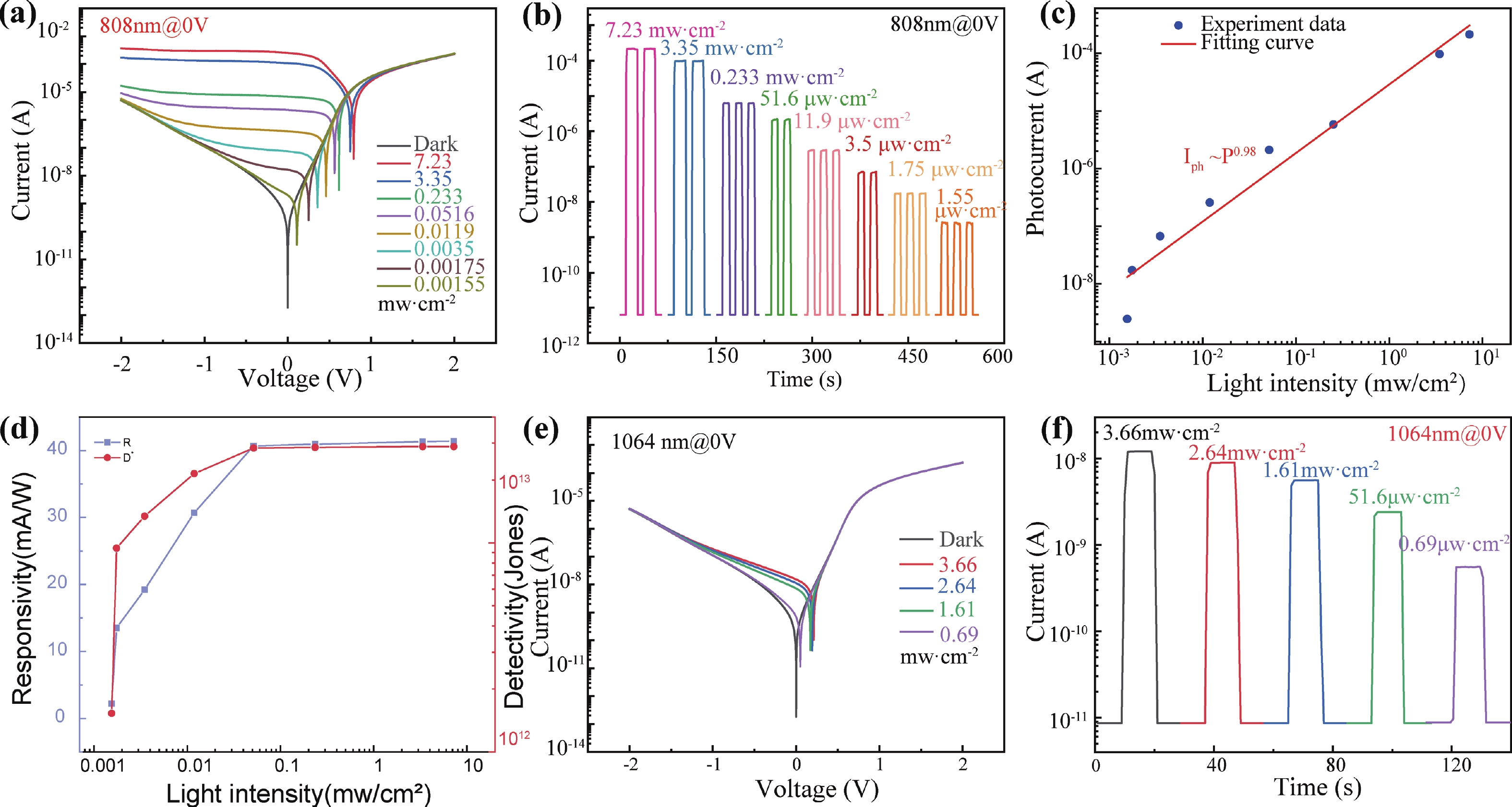
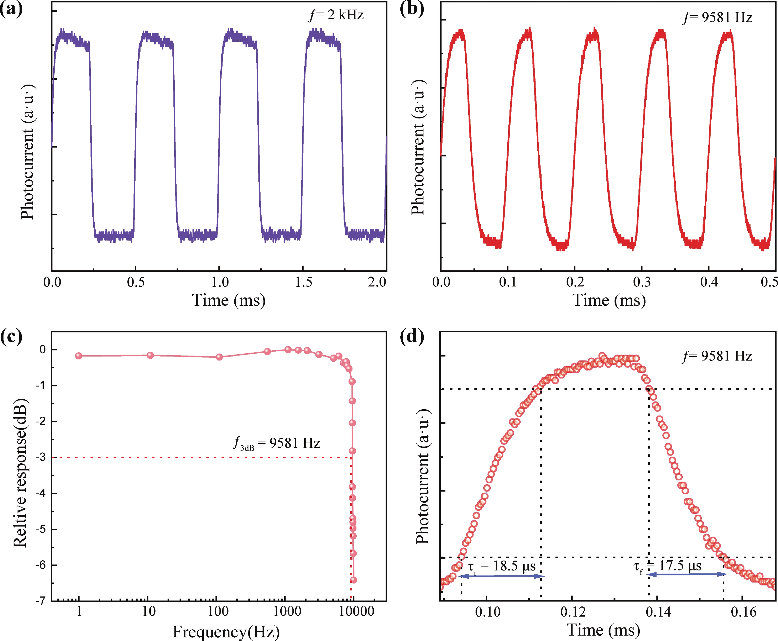
| [1] |
Lopez-Sanchez O, Lembke D, Kayci M, et al. Ultrasensitive photodetectors based on monolayer MoS 2. Nature Nanotech, 2013, 8, 497 doi: 10.1038/nnano.2013.100 |
| [2] |
Muench J, Ruocco A, Giambra M A, et al. Waveguide-integrated, plasmonic enhanced graphene photodetectors. Nano Lett, 2019, 19, 7632 doi: 10.1021/acs.nanolett.9b02238 |
| [3] |
Furchi M, Urich A, Pospischil A, et al. Microcavity-integrated graphene photodetector. Nano Lett, 2012, 12, 2773 doi: 10.1021/nl204512x |
| [4] |
Larki F, Abdi Y, Kameli P, et al. An effort towards full graphene photodetectors. Photonic Sens, 2022, 12, 31 doi: 10.1007/s13320-020-0600-7 |
| [5] |
|
| [6] |
He T, Ma H, Wang Z, et al. On-chip optoelectronic logic gates operating in the telecom band. Nat Photonics, 2024, 18, 60 doi: 10.1038/s41566-023-01309-7 |
| [7] |
Lee C M, Engelbrecht C J, Soper T D, et al. Scanning fiber endoscopy with highly flexible, 1 mm catheterscopes for wide-field, full-color imaging. J Biophotonics, 2010, 3, 385 doi: 10.1002/jbio.200900087 |
| [8] |
Wang Z, Tan C H, Peng M, et al. Giant infrared bulk photovoltaic effect in tellurene for broad-spectrum neuromodulation. Light Sci Appl, 2024, 13, 277 doi: 10.1038/s41377-024-01640-w |
| [9] |
Zhao T G, Guo J X, Li T, et al. Substrate engineering for wafer-scale two-dimensional material growth: strategies, mechanisms, and perspectives. Chem Soc Rev, 2023, 52, 1650 doi: 10.1039/D2CS00657J |
| [10] |
Qiu H, Yu Z H, Zhao T G, et al. Two-dimensional materials for future information technology: Status and prospects. Sci China Inf Sci, 2024, 67, 160400 doi: 10.1007/s11432-024-4033-8 |
| [11] |
Su W H, Zhang S, Liu C, et al. Interlayer transition induced infrared response in ReS 2/2D perovskite van der waals heterostructure photodetector. Nano Lett, 2022, 22, 10192 doi: 10.1021/acs.nanolett.2c04328 |
| [12] |
Radisavljevic B, Radenovic A, Brivio J, et al. Single-layer MoS 2 transistors. Nature Nanotech, 2011, 6, 147 doi: 10.1038/nnano.2010.279 |
| [13] |
Wang Q H, Kalantar-Zadeh K, Kis A, et al. Electronics and optoelectronics of two-dimensional transition metal dichalcogenides. Nature Nanotech, 2012, 7, 699 doi: 10.1038/nnano.2012.193 |
| [14] |
Chhowalla M, Jena D, Zhang H. Two-dimensional semiconductors for transistors. Nat Rev Mater, 2016, 1, 16052
|
| [15] |
Dou L T, Yang Y, You J B, et al. Solution-processed hybrid perovskite photodetectors with high detectivity. Nat Commun, 2014, 5, 5404 doi: 10.1038/ncomms6404 |
| [16] |
An X H, Liu F Z, Jung Y J, et al. Tunable graphene-silicon heterojunctions for ultrasensitive photodetection. Nano Lett, 2013, 13, 909 doi: 10.1021/nl303682j |
| [17] |
Goossens S, Navickaite G, Monasterio C, et al. Broadband image sensor array based on graphene–CMOS integration. Nat Photonics, 2017, 11, 366 doi: 10.1038/nphoton.2017.75 |
| [18] |
Ping J F, Fan Z X, Sindoro M, et al. Recent advances in sensing applications of two-dimensional transition metal dichalcogenide nanosheets and their composites. Adv Funct Mater, 2017, 27, 1605817 doi: 10.1002/adfm.201605817 |
| [19] |
Li J, Chen C, Liu S L, et al. Ultrafast electrochemical expansion of black phosphorus toward high-yield synthesis of few-layer phosphorene. Chem Mater, 2018, 30, 2742 doi: 10.1021/acs.chemmater.8b00521 |
| [20] |
Wang Y, Jaiswal M, Lin M, et al. Electronic properties of nanodiamond decorated graphene. ACS Nano, 2012, 6, 1018 doi: 10.1021/nn204362p |
| [21] |
Zhang B Y, Liu T, Meng B, et al. Broadband high photoresponse from pure monolayer graphene photodetector. Nat Commun, 2013, 4, 1811 doi: 10.1038/ncomms2830 |
| [22] |
Zhao T G, Chen Y, Xu T F, et al. Topological insulator Bi 2Se 3 heterojunction with a low dark current for midwave infrared photodetection. ACS Photonics, 2024, 11, 2450 doi: 10.1021/acsphotonics.4c00347 |
| [23] |
Bae S, Kim H, Lee Y, et al. Roll-to-roll production of 30-inch graphene films for transparent electrodes. Nat Nanotechnol, 2010, 5, 574 doi: 10.1038/nnano.2010.132 |
| [24] |
Fei Z, Rodin A S, Andreev G O, et al. Gate-tuning of graphene plasmons revealed by infrared nano-imaging. Nature, 2012, 487, 82 doi: 10.1038/nature11253 |
| [25] |
Xia F N, Wang H, Xiao D, et al. Two-dimensional material nanophotonics. Nature Photon, 2014, 8, 899 doi: 10.1038/nphoton.2014.271 |
| [26] |
Liu C S, Chen H W, Wang S Y, et al. Two-dimensional materials for next-generation computing technologies. Nat Nanotechnol, 2020, 15, 545 doi: 10.1038/s41565-020-0724-3 |
| [27] |
Liu Y, Huang Y, Duan X. Van der Waals integration before and beyond two-dimensional materials. Nature, 2019, 567, 323 doi: 10.1038/s41586-019-1013-x |
| [28] |
Luo L B, Hu H, Wang X H, et al. A graphene/GaAs near-infrared photodetector enabled by interfacial passivation with fast response and high sensitivity. J Mater Chem C, 2015, 3, 4723 doi: 10.1039/C5TC00449G |
| [29] |
Qu J, Chen J. Ag NPs and MoS 2 QDs double modified graphene/GaAs near-infrared photodetector. Semicond Sci Technol, 2023, 38, 055007 doi: 10.1088/1361-6641/acc3bc |
| [30] |
Wu J H, Yang Z W, Qiu C Y, et al. Enhanced performance of a graphene/GaAs self-driven near-infrared photodetector with upconversion nanoparticles. Nanoscale, 2018, 10, 8023 doi: 10.1039/C8NR00594J |
| [31] |
Cai Z L, He X Y, Wang K K, et al. Enhancing performance of GaN/Ga 2O 3 P-N junction uvc photodetectors via interdigitated structure. Small Methods, 2024, 8, e2301148 doi: 10.1002/smtd.202301148 |
| [32] |
Zeng L H, Lin S H, Li Z J, et al. Fast, self-driven, air-stable, and broadband photodetector based on vertically aligned PtSe 2/GaAs heterojunction. Adv Funct Mater, 2018, 28, 1705970 doi: 10.1002/adfm.201705970 |
| [33] |
Wang L, Jie J S, Shao Z B, et al. MoS 2 /Si heterojunction with vertically standing layered structure for ultrafast, high-detectivity, self-driven visible–near infrared photodetectors. Adv Funct Mater, 2015, 25, 2910 doi: 10.1002/adfm.201500216 |
| [34] |
Wang F, Zhang T, Xie R Z, et al. How to characterize figures of merit of two-dimensional photodetectors. Nat Commun, 2023, 14, 2224 doi: 10.1038/s41467-023-37635-1 |
| [35] |
Wang H. High gain single GaAs nanowire photodetector. Appl Phys Lett, 2013, 103, 093101
|
| [36] |
Wu J H, Qiu C Y, Feng S R, et al. A synergetic enhancement of localized surface plasmon resonance and photo-induced effect for graphene/GaAs photodetector. Nanotechnology, 2020, 31, 105204 doi: 10.1088/1361-6528/ab5a08 |


 Baorui Fang obtained his bachelor’s degree from Harbin University of Science and Technology in 2020. He is currently pursuing a master’s degree at Dalian University. His supervisors are Associate Professor Zongmin Ma and Researcher Xuechao Yu. His research mainly focuses on the design, fabrication, and characterization of infrared photodetectors.
 Zongmin Ma holds a Ph.D. in Solid Mechanics from Jilin University and completed postdoctoral research in Materials Science at Dalian University of Technology. His research focuses on medical devices, digital design, biomechanics, novel low-dimensional material optoelectronic devices, and additive manufacturing.
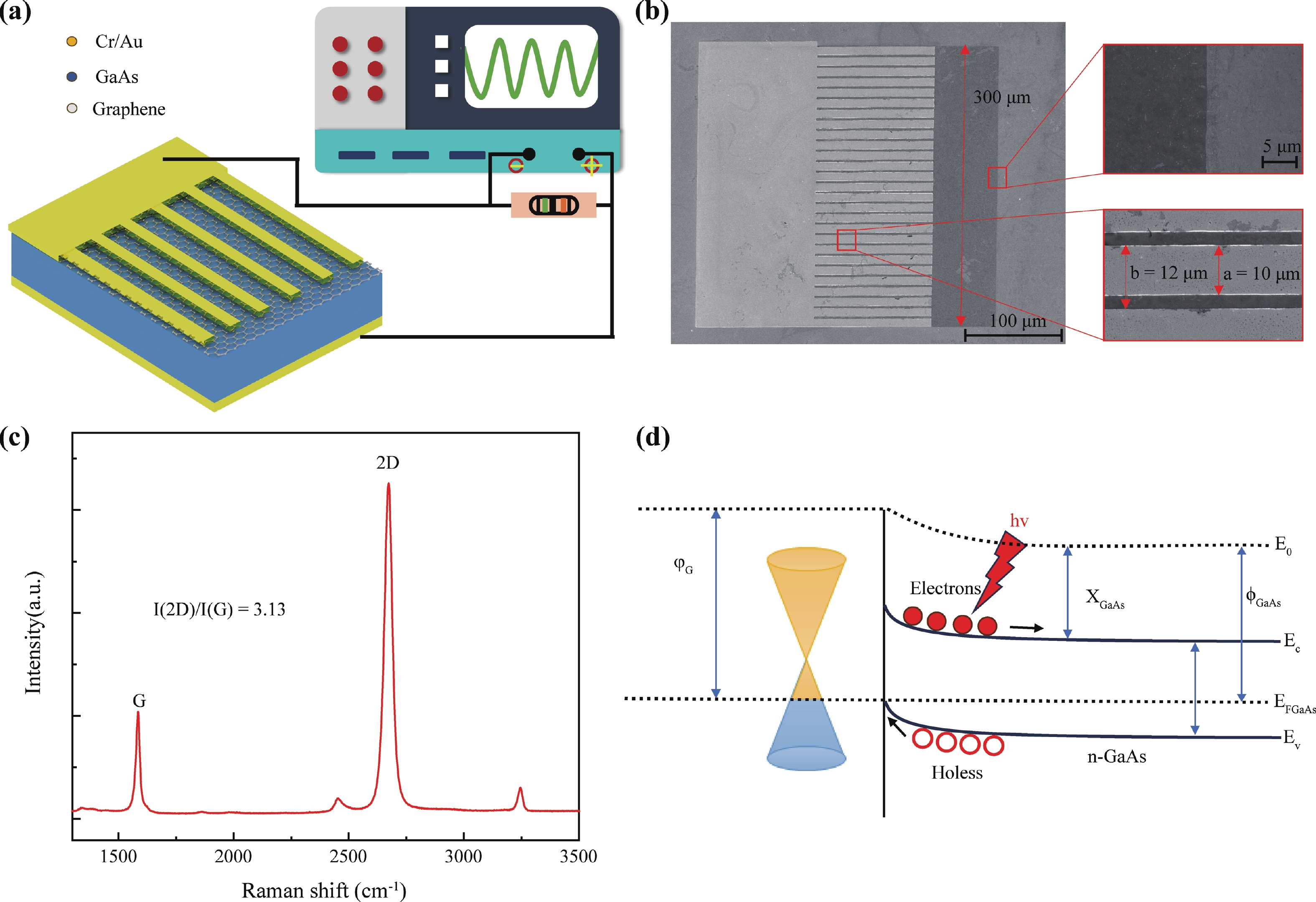
 DownLoad: