


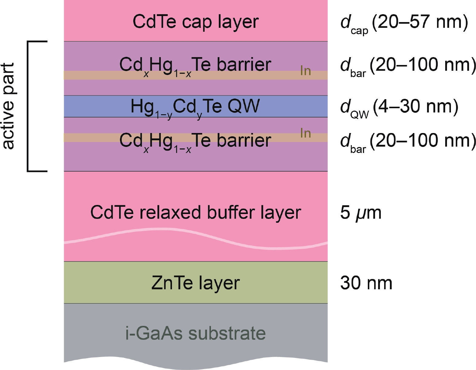
Fig. 1.
(Color online) Diagram of the structures under study. Indium doping layers are present only in some structures.
ARTICLES
Mikhail K. Sotnichuk1, Anton V. Ikonnikov1, , Dmitry R. Khokhlov1, Nikolay N. Mikhailov2, Sergey A. Dvoretsky2 and Vladimir I. Gavrilenko3
Corresponding author: Anton V. Ikonnikov, antikon@physics.msu.ru
Abstract: In this work, we studied the persistent photoconductivity (PPC) spectra in single HgTe/CdHgTe quantum wells with different growth parameters and different types of dark conductivity. The studies were performed in a wide radiation quantum energy range of 0.62–3.1 eV both at T = 4.2 K and at T = 77 K. Common features of the PPC spectra for all structures were revealed, and their relation to the presence of a CdTe cap layer in all structures and the appropriate cadmium fraction in the CdHgTe barrier layers was shown. One of the features was associated with the presence of a deep level in the CdTe layer. In addition, the oscillatory behavior of the PPC spectra in the region from 0.8–1.1 eV to 1.2–1.5 eV was observed. It is associated with the cascade emission of longitudinal optical phonons in CdHgTe barrier.
Keywords: quantum well, CdHgTe, persistent photoconductivity, heterostructure, spectroscopy
| [1] |
König M, Wiedmann S, Brüne C, et al. Quantum spin hall insulator state in HgTe quantum wells. Science, 2007, 318, 766 doi: 10.1126/science.1148047
|
| [2] |
Hasan M Z, Kane C L. Colloquium: Topological insulators. Rev Mod Phys, 2010, 82, 3045 doi: 10.1103/RevModPhys.82.3045
|
| [3] |
Fu L. Topological crystalline insulators. Phys Rev Lett, 2011, 106, 106802 doi: 10.1103/PhysRevLett.106.106802
|
| [4] |
Tanaka Y, Ren Z, Sato T, et al. Experimental realization of a topological crystalline insulator in SnTe. Nat Phys, 2012, 8, 800 doi: 10.1038/nphys2442
|
| [5] |
Tokura Y, Yasuda K, Tsukazaki A. Magnetic topological insulators. Nat Rev Phys, 2019, 1, 126 doi: 10.1038/s42254-018-0011-5
|
| [6] |
Schindler F, Cook A M, Vergniory M G, et al. Higher-order topological insulators. Sci Adv, 2018, 4, eaat0346 doi: 10.1126/sciadv.aat0346
|
| [7] |
Chen Y L, Analytis J G, Chu J H, et al. Experimental realization of a three-dimensional topological insulator, Bi2Te3. Science, 2009, 325, 178 doi: 10.1126/science.1173034
|
| [8] |
Kuroda K, Miyahara H, Ye M, et al. Experimental verification of PbBi2Te4 as a 3D topological insulator. Phys Rev Lett, 2012, 108, 206803 doi: 10.1103/PhysRevLett.108.206803
|
| [9] |
Liu C C, Feng W X, Yao Y G. Quantum spin Hall effect in silicene and two-dimensional germanium. Phys Rev Lett, 2011, 107, 076802 doi: 10.1103/PhysRevLett.107.076802
|
| [10] |
Zhou J J, Feng W X, Liu C C, et al. Large-gap quantum spin Hall insulator in single layer bismuth monobromide Bi4Br4. Nano Lett, 2014, 14, 4767 doi: 10.1021/nl501907g
|
| [11] |
Ma Y D, Kou L Z, Dai Y, et al. Proposed two-dimensional topological insulator in SiTe. Phys Rev B, 2016, 94, 201104(R doi: 10.1103/PhysRevB.94.201104
|
| [12] |
Knez I, Du R R, Sullivan G. Evidence for helical edge modes in inverted InAs/GaSb quantum wells. Phys Rev Lett, 2011, 107, 136603 doi: 10.1103/PhysRevLett.107.136603
|
| [13] |
Bampoulis P, Castenmiller C, Klaassen D J, et al. Quantum spin hall states and topological phase transition in germanene. Phys Rev Lett, 2023, 130, 196401 doi: 10.1103/PhysRevLett.130.196401
|
| [14] |
Wu S F, Fatemi V, Gibson Q D, et al. Observation of the quantum spin Hall effect up to 100 kelvin in a monolayer crystal. Science, 2018, 359, 76 doi: 10.1126/science.aan6003
|
| [15] |
Fei Z Y , Palomaki T, Wu S F, et al. Edge conduction in monolayer WTe2. Nat Phys, 2017, 13, 677 doi: 10.1038/nphys4091
|
| [16] |
Liu C, Culcer D, Wang Z N, et al. Helical edge transport in millimeter-scale thin films of Na3Bi. Nano Lett, 2020, 20, 6306 doi: 10.1021/acs.nanolett.0c01649
|
| [17] |
Lunczer L, Leubner P, Endres M, et al. Approaching quantization in macroscopic quantum spin hall devices through gate training. Phys Rev Lett, 2019, 123, 047701 doi: 10.1103/PhysRevLett.123.047701
|
| [18] |
Weber B, Fuhrer M S, Sheng X L, et al. 2024 roadmap on 2D topological insulators. J Phys Mater, 2024, 7, 022501 doi: 10.1088/2515-7639/ad2083
|
| [19] |
Krishtopenko S S, Yahniuk I, But D B, et al. Pressure- and temperature-driven phase transitions in HgTe quantum wells. Phys Rev B, 2016, 94, 245402 doi: 10.1103/PhysRevB.94.245402
|
| [20] |
Kvon Z D, Olshanetsky E B, Novik E G, et al. Two-dimensional electron-hole system in HgTe-based quantum wells with surface orientation (112). Phys Rev B, 2011, 83, 193304 doi: 10.1103/PhysRevB.83.193304
|
| [21] |
Bernevig B A, Zhang S C. Quantum spin Hall effect. Phys Rev Lett, 2006, 96, 106802 doi: 10.1103/PhysRevLett.96.106802
|
| [22] |
Kastalsky A, Hwang J C M. Study of persistent photoconductivity effect in n-type selectively doped AlGaAs/GaAs heterojunction. Solid State Commun, 1984, 51, 317 doi: 10.1016/0038-1098(84)90696-3
|
| [23] |
Anderson D A, Bass S J, Kane M J, et al. Transport and persistent photoconductivity in InGaAs/InP single quantum wells. Appl Phys Lett, 1986, 49, 1360 doi: 10.1063/1.97324
|
| [24] |
Tuttle G, Kroemer H, English J H. Electron concentrations and mobilities in AlSb/InAs/AlSb quantum wells. J Appl Phys, 1989, 65, 5239 doi: 10.1063/1.343167
|
| [25] |
Gauer C, Scriba J, Wixforth A, et al. Photoconductivity in AlSb/InAs quantum wells. Semicond Sci Technol, 1993, 8, S137 doi: 10.1088/0268-1242/8/1S/031
|
| [26] |
Lo I, Mitchel W C, Manasreh M O, et al. Negative persistent photoconductivity in the Al0.6Ga0.4Sb/InAs quantum wells. Appl Phys Lett, 1992, 60, 751 doi: 10.1063/1.106558
|
| [27] |
Chaves A S, Chacham H. Negative photoconductivity in semiconductor heterostructures. Appl Phys Lett, 1995, 66, 727 doi: 10.1063/1.114113
|
| [28] |
Tsai L C, Huang C F, Fan J C, et al. Persistent photoconductivity in SiGe/Si quantum wells. J Appl Phys, 1998, 84, 877 doi: 10.1063/1.368150
|
| [29] |
Wang W C, Tsai L C, Fan J C, et al. Positive and negative persistent photoconductivities in semimetallic Al xGa1– xSb/InAs quantum wells. J Appl Phys, 1999, 86, 3152 doi: 10.1063/1.371182
|
| [30] |
Aleshkin V Y, Gavrilenko V I, Gaponova D M, et al. Spectra of persistent photoconductivity in InAs/AlSb quantum-well heterostructures. Semicond, 2005, 39, 22 doi: 10.1134/1.1852637
|
| [31] |
Gavrilenko V I, Ikonnikov A V, Krishtopenko S S, et al. Persistent photoconductivity in InAs/AlSb heterostructures with double quantum wells. Semicond, 2010, 44, 616 doi: 10.1134/S106378261005012X
|
| [32] |
Spirin K E, Gaponova D M, Marem’yanin K V, et al. Bipolar persistent photoconductivity in HgTe/CdHgTe (013) double quantum-well heterostructures. Semicond, 2018, 52, 1586 doi: 10.1134/S1063782618120230
|
| [33] |
Spirin K E, Gaponova D M, Gavrilenko V I, et al. Residual-photoconductivity spectra in HgTe/CdHgTe quantum-well heterostructures. Semicond, 2019, 53, 1363 doi: 10.1134/S106378261910021X
|
| [34] |
Nikolaev I, Kazakov A, Drozdov K, et al. Bipolar persistent photoconductivity in HgTe/CdHgTe double quantum well heterostructures and its application for reversible change in the conductivity type. J Appl Phys, 2022, 132, 234301 doi: 10.1063/5.0121364
|
| [35] |
Sotnichuk M K, Kazakov A S, Nikolaev I D, et al. Cap layer effect on key features of persistent photoconductivity spectra in HgTe/CdHgTe double quantum well heterostructures. Photonics, 2023, 10, 877 doi: 10.3390/photonics10080877
|
| [36] |
Nikolaev I D, Uaman Svetikova T A, Rumyantsev V V, et al. Probing states of a double acceptor in CdHgTe heterostructures via optical gating. JETP Lett, 2020, 111, 575 doi: 10.1134/S0021364020100124
|
| [37] |
Shuvaev A, Dziom V, Gospodarič J, et al. Band structure near the Dirac point in HgTe quantum wells with critical thickness. Nanomaterials, 2022, 12, 2492 doi: 10.3390/nano12142492
|
| [38] |
Bovkun L S, Krishtopenko S S, Aleshkin V Y, et al. Simultaneous observation of the cyclotron resonances of electrons and holes in a HgTe/CdHgTe double quantum well under "optical gate" effect. JETP Lett, 2023, 118, 867 doi: 10.1134/S0021364023603536
|
| [39] |
Meyer M, Fähndrich T, Schmid S, et al. Coexistence of topological and normal insulating phases in electro-optically tuned InAs/GaSb bilayer quantum wells. Phys Rev B, 2024, 109, L121303 doi: 10.1103/PhysRevB.109.L121303
|
| [40] |
Mikhailov N N, Smirnov R N, Dvoretsky S A, et al. Growth of Hg1– xCd xTe nanostructures by molecular beam epitaxy with ellipsometric control. Int J Nanotechnol, 2006, 3, 120 doi: 10.1504/IJNT.2006.008725
|
| [41] |
Dvoretsky S, Mikhailov N, Sidorov Y, et al. Growth of HgTe quantum wells for IR to THz detectors. J Electron Mater, 2010, 39, 918 doi: 10.1007/s11664-010-1191-7
|
| [42] |
Bakhtin P A, Dvoretskii S A, Varavin V S, et al. Effect of low-temperature annealing on electrical properties of n-HgCdTe. Semiconductors, 2004, 38, 1172 doi: 10.1134/1.1808823
|
| [43] |
Ikonnikov A V, Zholudev M S, Marem’yanin K V, et al. Cyclotron resonance in HgTe/CdTe(013) narrowband heterostructures in quantized magnetic fields. JETP Lett, 2012, 95, 406 doi: 10.1134/S002136401208005X
|
| [44] |
Bovkun L S, Ikonnikov A V, Krishtopenko S S, et al. Effects of the electron—electron interaction in the magneto-absorption spectra of HgTe/CdHgTe quantum wells with an inverted band structure. JETP Lett, 2020, 112, 508 doi: 10.1134/S0021364020200059
|
| [45] |
Bovkun L S, Ikonnikov A V, Aleshkin V Y, et al. Magnetospectroscopy of double HgTe/CdHgTe QWs with inverted band structure in high magnetic fields up to 30 T. Opto Electron Rev, 2019, 27, 213 doi: 10.1016/j.opelre.2019.06.001
|
| [46] |
Ikonnikov A V, Bovkun L S, Rumyantsev V V, et al. On the band spectrum in p-type HgTe/CdHgTe heterostructures and its transformation under temperature variation. Semicond, 2017, 51, 1531 doi: 10.1134/S1063782617120090
|
| [47] |
Laurenti J P, Camassel J, Bouhemadou A, et al. Temperature dependence of the fundamental absorption edge of mercury cadmium telluride. J Appl Phys, 1990, 67, 6454 doi: 10.1063/1.345119
|
| [48] |
Novik E G, Pfeuffer-Jeschke A, Jungwirth T, et al. Band structure of semimagnetic Hg1– yMn yTe quantum wells. Phys Rev B, 2005, 72, 035321 doi: 10.1103/PhysRevB.72.035321
|
| [49] |
Yakunin M V, Krishtopenko S S, Desrat W, et al. Unconventional reentrant quantum hall effect in a HgTe/CdHgTe double quantum well. Phys Rev B, 2020, 102, 165305 doi: 10.1103/PhysRevB.102.165305
|
| [50] |
Ikonnikov A V, Krishtopenko S S, Bovkun L S, et al. Origin of structure inversion asymmetry in double HgTe quantum wells. JETP Lett, 2022, 116, 547 doi: 10.1134/S0021364022601889
|
| [51] |
Khattak G M, Scott C G. Characteristics of deep levels in n-type CdTe. J Phys: Condens Matter, 1991, 3, 8619 doi: 10.1088/0953-8984/3/44/008
|
| [52] |
Castaldini A, Cavallini A, Fraboni B, et al. Deep energy levels in CdTe and CdZnTe. J Appl Phys, 1998, 83, 2121 doi: 10.1063/1.366946
|
| [53] |
Cardona M, Greenaway D L. Fundamental reflectivity and band structure of ZnTe, CdTe, and HgTe. Phys Rev, 1963, 131, 98 doi: 10.1103/PhysRev.131.98
|
| [54] |
Chadi D J, Walter J P, Cohen M L, et al. Reflectivities and electronic band structures of CdTe and HgTe. Phys Rev B, 1972, 5, 3058 doi: 10.1103/PhysRevB.5.3058
|
| [55] |
Shaw R W. Intrinsic oscillatory photoconductivity and the band structure of GaAs. Phys Rev B, 1971, 3, 3283 doi: 10.1103/PhysRevB.3.3283
|
| [56] |
Nicholas R J, Carter A C, Fung S, et al. A study of the energy loss mechanisms for hot electrons in CdTe and CdS from oscillatory photoconductivity and the magnetophonon effect. J Phys C Solid State Phys, 1980, 13, 5215 doi: 10.1088/0022-3719/13/28/009
|
| [57] |
Kartheuser E, Schmit J, Evrard R. Theory of extrinsic oscillatory photoconductivity in polar semiconductors. J Appl Phys, 1988, 63, 784 doi: 10.1063/1.340070
|
| [58] |
Talwar D N, Vandevyver M. Vibrational properties of HgCdTe system. J Appl Phys, 1984, 56, 1601 doi: 10.1063/1.334144
|
| [59] |
Weiler M H. Chapter 3 Magnetooptical properties of Hg1-xCdx Te alloys. Semiconductors and semimetals. Amsterdam: Elsevier, 1981, 119 doi: 10.1016/S0080-8784(08)60130-1
|
| [60] |
Bhan R K, Dhar V. Carrier density approximation for non-parabolic and highly degenerate HgCdTe semiconductors. Semicond Sci Technol, 2004, 19, 413 doi: 10.1088/0268-1242/19/3/021
|
| [61] |
Xie R Z , Li Q, Wang P, et al. Spatial description theory of narrow-band single-carrier avalanche photodetectors. Opt Express, 2021, 29, 16432 doi: 10.1364/OE.418110
|
| [62] |
Ikonnikov A V, Zholudev M S, Gavrilenko V I, et al. Magnetoabsorption in narrow-gap HgCdTe epitaxial layers in the terahertz range. Semicond, 2013, 47, 1545 doi: 10.1134/S1063782613120099
|
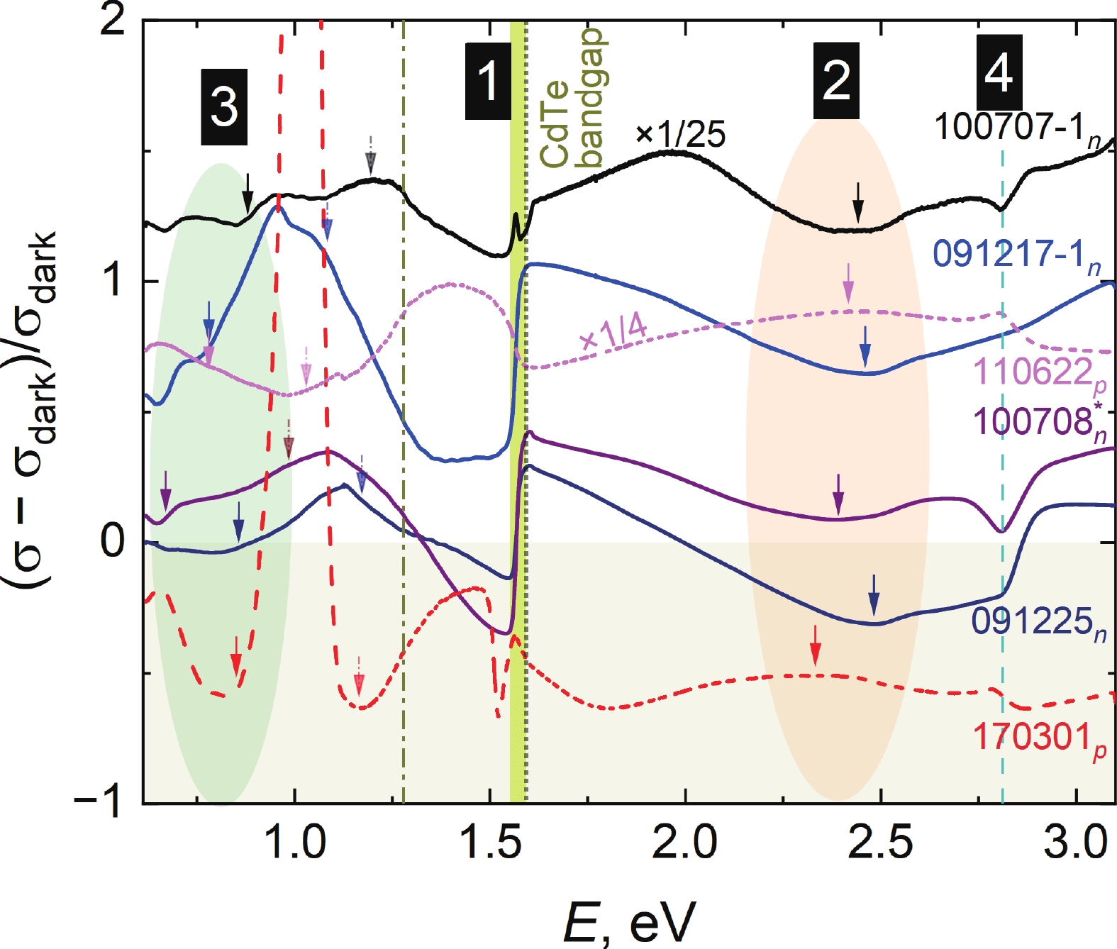
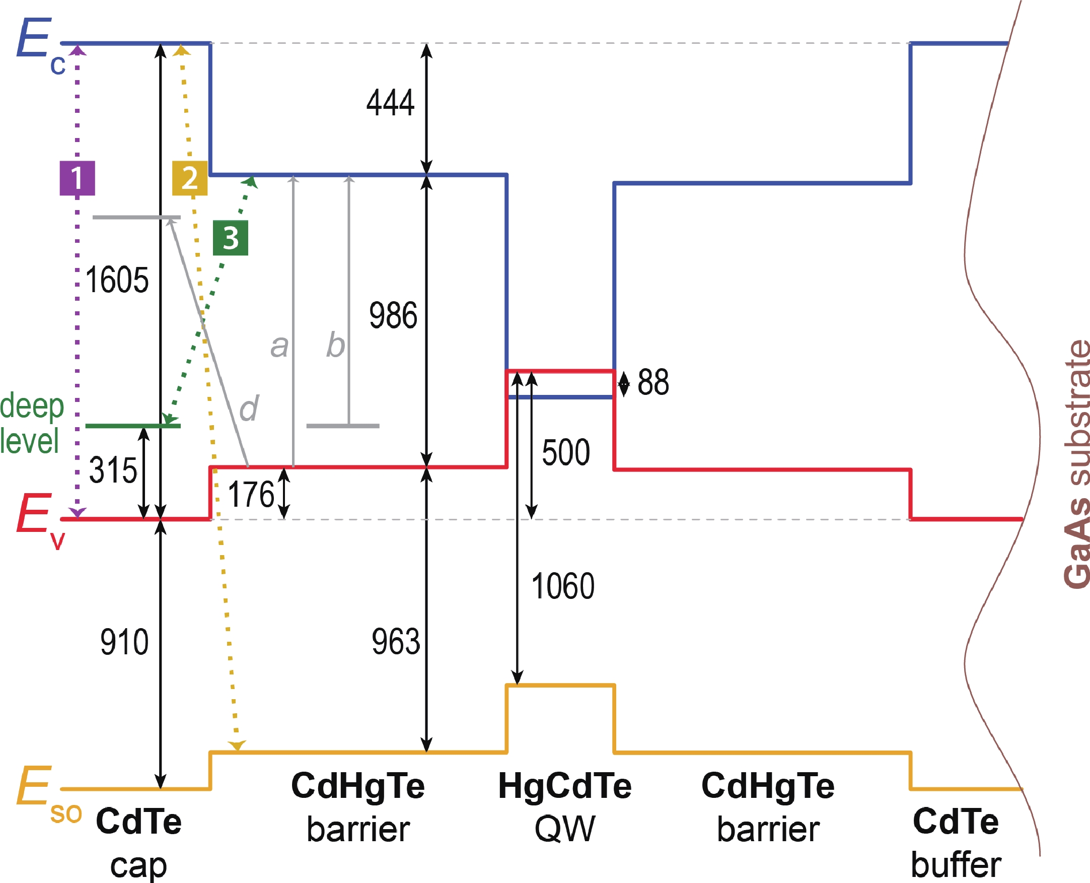
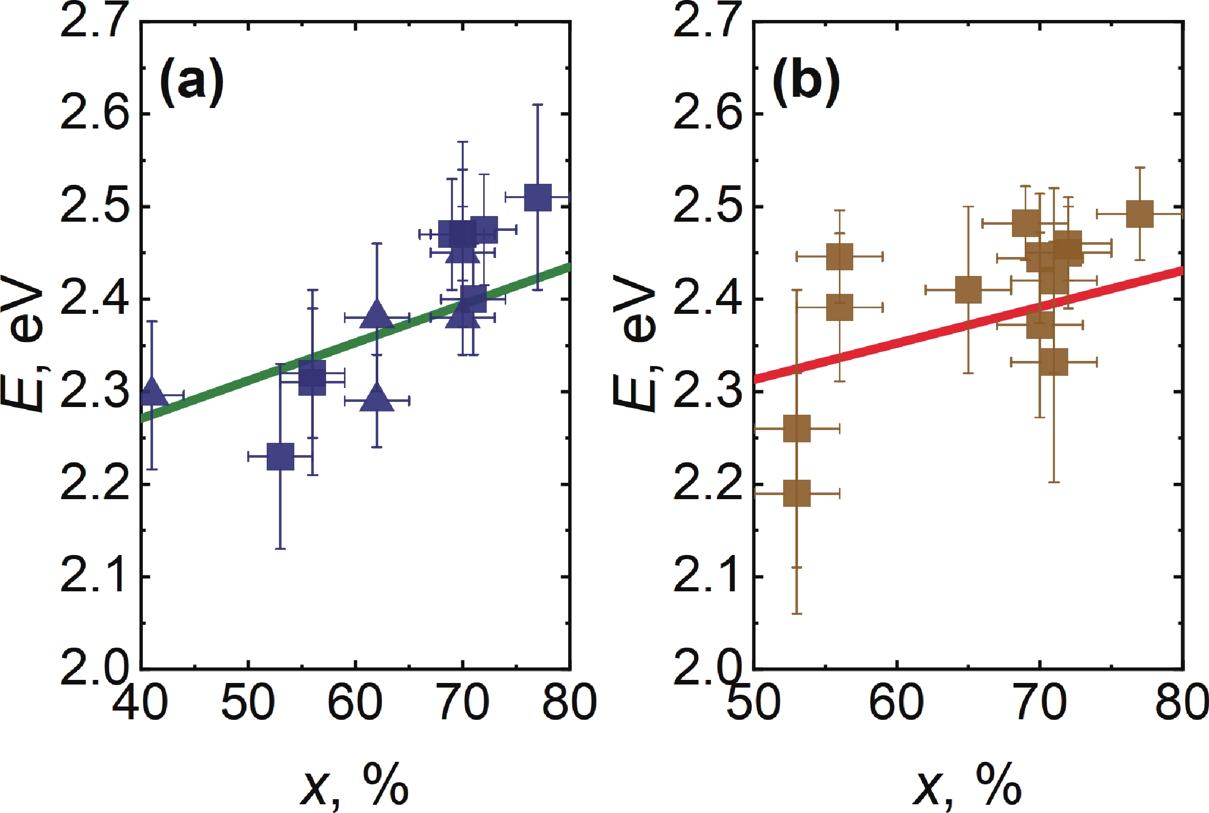
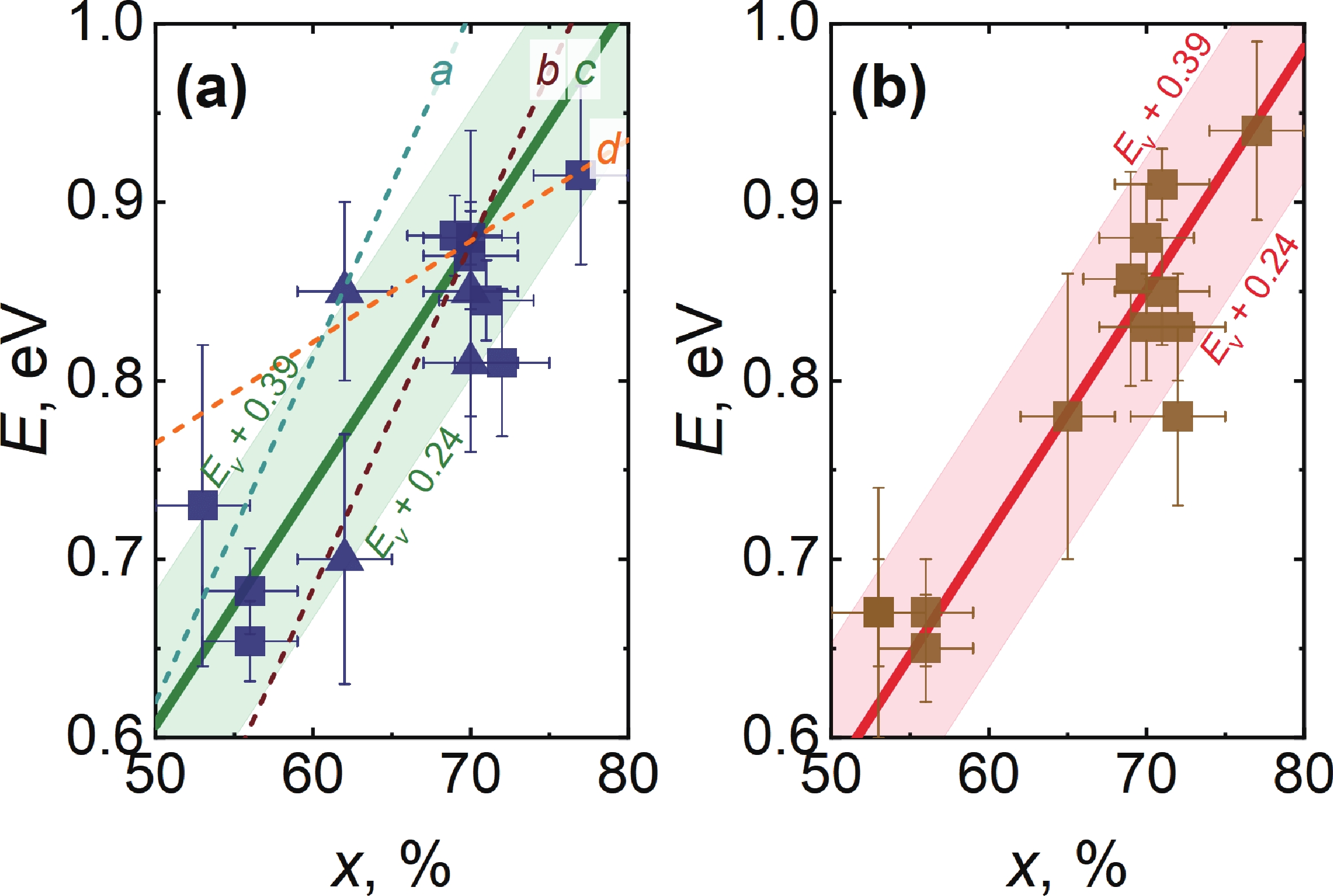
Table 1. Parameters of the structures under study. The parameters specified based on the results of measuring the magnetoabsorption spectra and/or photoconductivity spectra at different temperatures are given in brackets. An asterisk in the number means that the structure was annealed, which should lead to the formation of additional acceptors (mercury vacancies). The subscript in the number indicates the type of low-temperature dark conductivity. Band spectrum types: N—normal, GL—gapless, I—inverted. Rdark—resistance of the sample after cooling in the absence of special illumination. n (p) is the 'dark' concentration and type of charge carriers, μn (μp) is the corresponding mobility.
| Structure | dQW (nm) |
y (%) | dbar (nm) |
x (%) | In doped | Annealed | dcap (nm) |
Band structure |
n (p) (1011 cm–2) (T = 4.2 К) |
μn (μp) (103 cm2/(V·s)) (T = 4.2 К) |
Rdark (kΩ) (T = 4.2 К) |
Rdark (kΩ) (T = 77 K) |
| 101109n | 8 | 0 | 60 | 77 | √ | 50 | I | 5 (n) | 100 | 0.05 | 0.05 | |
| 091217-1n | 7 | 0 | 33 | 72 | √ | 40 | I | 1.8 (n) | 50 | 3.7 | 1.43 | |
| 091225n | 30 | 18 (12) | 100 | 69 | 50 | GL | 0.05 (n) | 600 | 2.24 | 0.83 | ||
| 091225-1 | 30 | 18 (13) | 100 | 72 | 50 | N | Insulator | Insulator | 300 | 1.8 | ||
| 100708n | 30 | 16 (13) | 100 | 56 | 57 | GL | 0.7 (n) | 480 | 0.3 | 0.29 | ||
| 100708*n | 30 | 16 (13) | 100 | 56 | √ | 57 | GL | 1.8 (n) | 45 | 1.4 | 0.8 | |
| 100707-1 | 30 | 19 | 100 | 70 | 50 | N | Insulator | Insulator | 150 | 100 | ||
| 100707-1* | 30 | 19 | 100 | 70 | √ | 50 | N | Insulator | Insulator | 140 | 70 | |
| 170301p | 9 | 0 (8) | 30 | 71 | 50 | N | 0.3 (p) | 3.7 | 80 | 62 | ||
| 170303p | 9 | 10 | 30 | 71 | 50 | N | 0.5 (p) | 3 | 30 | 56 | ||
| 130410p | 5 (4) | 0 | 20 | 53 | 20 | N | 2 (p) | 0.3 | 70 | 600 | ||
| 130410*p | 5 (4) | 0 | 20 | 53 | √ | 20 | N | 1.9 (p) | 0.2 | 81 | 170 | |
| 110622p | 5.6 (4.6) | 0 | 35 | 65 | 40 | N | 0.9 (p) | 9 | 5 | 1500 |
 DownLoad: CSV
| [1] |
König M, Wiedmann S, Brüne C, et al. Quantum spin hall insulator state in HgTe quantum wells. Science, 2007, 318, 766 doi: 10.1126/science.1148047
|
| [2] |
Hasan M Z, Kane C L. Colloquium: Topological insulators. Rev Mod Phys, 2010, 82, 3045 doi: 10.1103/RevModPhys.82.3045
|
| [3] |
Fu L. Topological crystalline insulators. Phys Rev Lett, 2011, 106, 106802 doi: 10.1103/PhysRevLett.106.106802
|
| [4] |
Tanaka Y, Ren Z, Sato T, et al. Experimental realization of a topological crystalline insulator in SnTe. Nat Phys, 2012, 8, 800 doi: 10.1038/nphys2442
|
| [5] |
Tokura Y, Yasuda K, Tsukazaki A. Magnetic topological insulators. Nat Rev Phys, 2019, 1, 126 doi: 10.1038/s42254-018-0011-5
|
| [6] |
Schindler F, Cook A M, Vergniory M G, et al. Higher-order topological insulators. Sci Adv, 2018, 4, eaat0346 doi: 10.1126/sciadv.aat0346
|
| [7] |
Chen Y L, Analytis J G, Chu J H, et al. Experimental realization of a three-dimensional topological insulator, Bi2Te3. Science, 2009, 325, 178 doi: 10.1126/science.1173034
|
| [8] |
Kuroda K, Miyahara H, Ye M, et al. Experimental verification of PbBi2Te4 as a 3D topological insulator. Phys Rev Lett, 2012, 108, 206803 doi: 10.1103/PhysRevLett.108.206803
|
| [9] |
Liu C C, Feng W X, Yao Y G. Quantum spin Hall effect in silicene and two-dimensional germanium. Phys Rev Lett, 2011, 107, 076802 doi: 10.1103/PhysRevLett.107.076802
|
| [10] |
Zhou J J, Feng W X, Liu C C, et al. Large-gap quantum spin Hall insulator in single layer bismuth monobromide Bi4Br4. Nano Lett, 2014, 14, 4767 doi: 10.1021/nl501907g
|
| [11] |
Ma Y D, Kou L Z, Dai Y, et al. Proposed two-dimensional topological insulator in SiTe. Phys Rev B, 2016, 94, 201104(R doi: 10.1103/PhysRevB.94.201104
|
| [12] |
Knez I, Du R R, Sullivan G. Evidence for helical edge modes in inverted InAs/GaSb quantum wells. Phys Rev Lett, 2011, 107, 136603 doi: 10.1103/PhysRevLett.107.136603
|
| [13] |
Bampoulis P, Castenmiller C, Klaassen D J, et al. Quantum spin hall states and topological phase transition in germanene. Phys Rev Lett, 2023, 130, 196401 doi: 10.1103/PhysRevLett.130.196401
|
| [14] |
Wu S F, Fatemi V, Gibson Q D, et al. Observation of the quantum spin Hall effect up to 100 kelvin in a monolayer crystal. Science, 2018, 359, 76 doi: 10.1126/science.aan6003
|
| [15] |
Fei Z Y , Palomaki T, Wu S F, et al. Edge conduction in monolayer WTe2. Nat Phys, 2017, 13, 677 doi: 10.1038/nphys4091
|
| [16] |
Liu C, Culcer D, Wang Z N, et al. Helical edge transport in millimeter-scale thin films of Na3Bi. Nano Lett, 2020, 20, 6306 doi: 10.1021/acs.nanolett.0c01649
|
| [17] |
Lunczer L, Leubner P, Endres M, et al. Approaching quantization in macroscopic quantum spin hall devices through gate training. Phys Rev Lett, 2019, 123, 047701 doi: 10.1103/PhysRevLett.123.047701
|
| [18] |
Weber B, Fuhrer M S, Sheng X L, et al. 2024 roadmap on 2D topological insulators. J Phys Mater, 2024, 7, 022501 doi: 10.1088/2515-7639/ad2083
|
| [19] |
Krishtopenko S S, Yahniuk I, But D B, et al. Pressure- and temperature-driven phase transitions in HgTe quantum wells. Phys Rev B, 2016, 94, 245402 doi: 10.1103/PhysRevB.94.245402
|
| [20] |
Kvon Z D, Olshanetsky E B, Novik E G, et al. Two-dimensional electron-hole system in HgTe-based quantum wells with surface orientation (112). Phys Rev B, 2011, 83, 193304 doi: 10.1103/PhysRevB.83.193304
|
| [21] |
Bernevig B A, Zhang S C. Quantum spin Hall effect. Phys Rev Lett, 2006, 96, 106802 doi: 10.1103/PhysRevLett.96.106802
|
| [22] |
Kastalsky A, Hwang J C M. Study of persistent photoconductivity effect in n-type selectively doped AlGaAs/GaAs heterojunction. Solid State Commun, 1984, 51, 317 doi: 10.1016/0038-1098(84)90696-3
|
| [23] |
Anderson D A, Bass S J, Kane M J, et al. Transport and persistent photoconductivity in InGaAs/InP single quantum wells. Appl Phys Lett, 1986, 49, 1360 doi: 10.1063/1.97324
|
| [24] |
Tuttle G, Kroemer H, English J H. Electron concentrations and mobilities in AlSb/InAs/AlSb quantum wells. J Appl Phys, 1989, 65, 5239 doi: 10.1063/1.343167
|
| [25] |
Gauer C, Scriba J, Wixforth A, et al. Photoconductivity in AlSb/InAs quantum wells. Semicond Sci Technol, 1993, 8, S137 doi: 10.1088/0268-1242/8/1S/031
|
| [26] |
Lo I, Mitchel W C, Manasreh M O, et al. Negative persistent photoconductivity in the Al0.6Ga0.4Sb/InAs quantum wells. Appl Phys Lett, 1992, 60, 751 doi: 10.1063/1.106558
|
| [27] |
Chaves A S, Chacham H. Negative photoconductivity in semiconductor heterostructures. Appl Phys Lett, 1995, 66, 727 doi: 10.1063/1.114113
|
| [28] |
Tsai L C, Huang C F, Fan J C, et al. Persistent photoconductivity in SiGe/Si quantum wells. J Appl Phys, 1998, 84, 877 doi: 10.1063/1.368150
|
| [29] |
Wang W C, Tsai L C, Fan J C, et al. Positive and negative persistent photoconductivities in semimetallic Al xGa1– xSb/InAs quantum wells. J Appl Phys, 1999, 86, 3152 doi: 10.1063/1.371182
|
| [30] |
Aleshkin V Y, Gavrilenko V I, Gaponova D M, et al. Spectra of persistent photoconductivity in InAs/AlSb quantum-well heterostructures. Semicond, 2005, 39, 22 doi: 10.1134/1.1852637
|
| [31] |
Gavrilenko V I, Ikonnikov A V, Krishtopenko S S, et al. Persistent photoconductivity in InAs/AlSb heterostructures with double quantum wells. Semicond, 2010, 44, 616 doi: 10.1134/S106378261005012X
|
| [32] |
Spirin K E, Gaponova D M, Marem’yanin K V, et al. Bipolar persistent photoconductivity in HgTe/CdHgTe (013) double quantum-well heterostructures. Semicond, 2018, 52, 1586 doi: 10.1134/S1063782618120230
|
| [33] |
Spirin K E, Gaponova D M, Gavrilenko V I, et al. Residual-photoconductivity spectra in HgTe/CdHgTe quantum-well heterostructures. Semicond, 2019, 53, 1363 doi: 10.1134/S106378261910021X
|
| [34] |
Nikolaev I, Kazakov A, Drozdov K, et al. Bipolar persistent photoconductivity in HgTe/CdHgTe double quantum well heterostructures and its application for reversible change in the conductivity type. J Appl Phys, 2022, 132, 234301 doi: 10.1063/5.0121364
|
| [35] |
Sotnichuk M K, Kazakov A S, Nikolaev I D, et al. Cap layer effect on key features of persistent photoconductivity spectra in HgTe/CdHgTe double quantum well heterostructures. Photonics, 2023, 10, 877 doi: 10.3390/photonics10080877
|
| [36] |
Nikolaev I D, Uaman Svetikova T A, Rumyantsev V V, et al. Probing states of a double acceptor in CdHgTe heterostructures via optical gating. JETP Lett, 2020, 111, 575 doi: 10.1134/S0021364020100124
|
| [37] |
Shuvaev A, Dziom V, Gospodarič J, et al. Band structure near the Dirac point in HgTe quantum wells with critical thickness. Nanomaterials, 2022, 12, 2492 doi: 10.3390/nano12142492
|
| [38] |
Bovkun L S, Krishtopenko S S, Aleshkin V Y, et al. Simultaneous observation of the cyclotron resonances of electrons and holes in a HgTe/CdHgTe double quantum well under "optical gate" effect. JETP Lett, 2023, 118, 867 doi: 10.1134/S0021364023603536
|
| [39] |
Meyer M, Fähndrich T, Schmid S, et al. Coexistence of topological and normal insulating phases in electro-optically tuned InAs/GaSb bilayer quantum wells. Phys Rev B, 2024, 109, L121303 doi: 10.1103/PhysRevB.109.L121303
|
| [40] |
Mikhailov N N, Smirnov R N, Dvoretsky S A, et al. Growth of Hg1– xCd xTe nanostructures by molecular beam epitaxy with ellipsometric control. Int J Nanotechnol, 2006, 3, 120 doi: 10.1504/IJNT.2006.008725
|
| [41] |
Dvoretsky S, Mikhailov N, Sidorov Y, et al. Growth of HgTe quantum wells for IR to THz detectors. J Electron Mater, 2010, 39, 918 doi: 10.1007/s11664-010-1191-7
|
| [42] |
Bakhtin P A, Dvoretskii S A, Varavin V S, et al. Effect of low-temperature annealing on electrical properties of n-HgCdTe. Semiconductors, 2004, 38, 1172 doi: 10.1134/1.1808823
|
| [43] |
Ikonnikov A V, Zholudev M S, Marem’yanin K V, et al. Cyclotron resonance in HgTe/CdTe(013) narrowband heterostructures in quantized magnetic fields. JETP Lett, 2012, 95, 406 doi: 10.1134/S002136401208005X
|
| [44] |
Bovkun L S, Ikonnikov A V, Krishtopenko S S, et al. Effects of the electron—electron interaction in the magneto-absorption spectra of HgTe/CdHgTe quantum wells with an inverted band structure. JETP Lett, 2020, 112, 508 doi: 10.1134/S0021364020200059
|
| [45] |
Bovkun L S, Ikonnikov A V, Aleshkin V Y, et al. Magnetospectroscopy of double HgTe/CdHgTe QWs with inverted band structure in high magnetic fields up to 30 T. Opto Electron Rev, 2019, 27, 213 doi: 10.1016/j.opelre.2019.06.001
|
| [46] |
Ikonnikov A V, Bovkun L S, Rumyantsev V V, et al. On the band spectrum in p-type HgTe/CdHgTe heterostructures and its transformation under temperature variation. Semicond, 2017, 51, 1531 doi: 10.1134/S1063782617120090
|
| [47] |
Laurenti J P, Camassel J, Bouhemadou A, et al. Temperature dependence of the fundamental absorption edge of mercury cadmium telluride. J Appl Phys, 1990, 67, 6454 doi: 10.1063/1.345119
|
| [48] |
Novik E G, Pfeuffer-Jeschke A, Jungwirth T, et al. Band structure of semimagnetic Hg1– yMn yTe quantum wells. Phys Rev B, 2005, 72, 035321 doi: 10.1103/PhysRevB.72.035321
|
| [49] |
Yakunin M V, Krishtopenko S S, Desrat W, et al. Unconventional reentrant quantum hall effect in a HgTe/CdHgTe double quantum well. Phys Rev B, 2020, 102, 165305 doi: 10.1103/PhysRevB.102.165305
|
| [50] |
Ikonnikov A V, Krishtopenko S S, Bovkun L S, et al. Origin of structure inversion asymmetry in double HgTe quantum wells. JETP Lett, 2022, 116, 547 doi: 10.1134/S0021364022601889
|
| [51] |
Khattak G M, Scott C G. Characteristics of deep levels in n-type CdTe. J Phys: Condens Matter, 1991, 3, 8619 doi: 10.1088/0953-8984/3/44/008
|
| [52] |
Castaldini A, Cavallini A, Fraboni B, et al. Deep energy levels in CdTe and CdZnTe. J Appl Phys, 1998, 83, 2121 doi: 10.1063/1.366946
|
| [53] |
Cardona M, Greenaway D L. Fundamental reflectivity and band structure of ZnTe, CdTe, and HgTe. Phys Rev, 1963, 131, 98 doi: 10.1103/PhysRev.131.98
|
| [54] |
Chadi D J, Walter J P, Cohen M L, et al. Reflectivities and electronic band structures of CdTe and HgTe. Phys Rev B, 1972, 5, 3058 doi: 10.1103/PhysRevB.5.3058
|
| [55] |
Shaw R W. Intrinsic oscillatory photoconductivity and the band structure of GaAs. Phys Rev B, 1971, 3, 3283 doi: 10.1103/PhysRevB.3.3283
|
| [56] |
Nicholas R J, Carter A C, Fung S, et al. A study of the energy loss mechanisms for hot electrons in CdTe and CdS from oscillatory photoconductivity and the magnetophonon effect. J Phys C Solid State Phys, 1980, 13, 5215 doi: 10.1088/0022-3719/13/28/009
|
| [57] |
Kartheuser E, Schmit J, Evrard R. Theory of extrinsic oscillatory photoconductivity in polar semiconductors. J Appl Phys, 1988, 63, 784 doi: 10.1063/1.340070
|
| [58] |
Talwar D N, Vandevyver M. Vibrational properties of HgCdTe system. J Appl Phys, 1984, 56, 1601 doi: 10.1063/1.334144
|
| [59] |
Weiler M H. Chapter 3 Magnetooptical properties of Hg1-xCdx Te alloys. Semiconductors and semimetals. Amsterdam: Elsevier, 1981, 119 doi: 10.1016/S0080-8784(08)60130-1
|
| [60] |
Bhan R K, Dhar V. Carrier density approximation for non-parabolic and highly degenerate HgCdTe semiconductors. Semicond Sci Technol, 2004, 19, 413 doi: 10.1088/0268-1242/19/3/021
|
| [61] |
Xie R Z , Li Q, Wang P, et al. Spatial description theory of narrow-band single-carrier avalanche photodetectors. Opt Express, 2021, 29, 16432 doi: 10.1364/OE.418110
|
| [62] |
Ikonnikov A V, Zholudev M S, Gavrilenko V I, et al. Magnetoabsorption in narrow-gap HgCdTe epitaxial layers in the terahertz range. Semicond, 2013, 47, 1545 doi: 10.1134/S1063782613120099
|


Article views: 1533 Times PDF downloads: 65 Times Cited by: 0 Times
Received: 10 September 2024 Revised: 03 December 2024 Online: Accepted Manuscript: 23 December 2024Uncorrected proof: 26 February 2025Published: 10 April 2025
| Citation: |
Mikhail K. Sotnichuk, Anton V. Ikonnikov, Dmitry R. Khokhlov, Nikolay N. Mikhailov, Sergey A. Dvoretsky, Vladimir I. Gavrilenko. Features of persistent photoconductivity in CdHgTe-based single quantum well heterostructures[J]. Journal of Semiconductors, 2025, 46(4): 042702. doi: 10.1088/1674-4926/24090023
****
M K Sotnichuk, A V Ikonnikov, D R Khokhlov, N N Mikhailov, S A Dvoretsky, and V I Gavrilenko, Features of persistent photoconductivity in CdHgTe-based single quantum well heterostructures[J]. J. Semicond., 2025, 46(4), 042702 doi: 10.1088/1674-4926/24090023

|
 Mikhail K. Sotnichuk is currently a student of the Faculty of Physics of Lomonosov Moscow State University (graduation year 2027). His research interests include narrow-band quantum well heterostructures, photoconductivity and persistent photoconductivity effects
 Anton V. Ikonnikov received his PhD in Physics and Mathematics from the Institute of Physics of Microstructures of the Russian Academy of Sciences (Nizhny Novgorod, Russia) in 2006. He is currently a senior research fellow at the Faculty of Physics of Lomonosov Moscow State University. His research focuses on the spectroscopy of both bulk and two-dimensional systems based on narrow-gap semiconductors. He is also involved in the research and development of terahertz quantum cascade lasers
| [1] |
König M, Wiedmann S, Brüne C, et al. Quantum spin hall insulator state in HgTe quantum wells. Science, 2007, 318, 766 doi: 10.1126/science.1148047
|
| [2] |
Hasan M Z, Kane C L. Colloquium: Topological insulators. Rev Mod Phys, 2010, 82, 3045 doi: 10.1103/RevModPhys.82.3045
|
| [3] |
Fu L. Topological crystalline insulators. Phys Rev Lett, 2011, 106, 106802 doi: 10.1103/PhysRevLett.106.106802
|
| [4] |
Tanaka Y, Ren Z, Sato T, et al. Experimental realization of a topological crystalline insulator in SnTe. Nat Phys, 2012, 8, 800 doi: 10.1038/nphys2442
|
| [5] |
Tokura Y, Yasuda K, Tsukazaki A. Magnetic topological insulators. Nat Rev Phys, 2019, 1, 126 doi: 10.1038/s42254-018-0011-5
|
| [6] |
Schindler F, Cook A M, Vergniory M G, et al. Higher-order topological insulators. Sci Adv, 2018, 4, eaat0346 doi: 10.1126/sciadv.aat0346
|
| [7] |
Chen Y L, Analytis J G, Chu J H, et al. Experimental realization of a three-dimensional topological insulator, Bi2Te3. Science, 2009, 325, 178 doi: 10.1126/science.1173034
|
| [8] |
Kuroda K, Miyahara H, Ye M, et al. Experimental verification of PbBi2Te4 as a 3D topological insulator. Phys Rev Lett, 2012, 108, 206803 doi: 10.1103/PhysRevLett.108.206803
|
| [9] |
Liu C C, Feng W X, Yao Y G. Quantum spin Hall effect in silicene and two-dimensional germanium. Phys Rev Lett, 2011, 107, 076802 doi: 10.1103/PhysRevLett.107.076802
|
| [10] |
Zhou J J, Feng W X, Liu C C, et al. Large-gap quantum spin Hall insulator in single layer bismuth monobromide Bi4Br4. Nano Lett, 2014, 14, 4767 doi: 10.1021/nl501907g
|
| [11] |
Ma Y D, Kou L Z, Dai Y, et al. Proposed two-dimensional topological insulator in SiTe. Phys Rev B, 2016, 94, 201104(R doi: 10.1103/PhysRevB.94.201104
|
| [12] |
Knez I, Du R R, Sullivan G. Evidence for helical edge modes in inverted InAs/GaSb quantum wells. Phys Rev Lett, 2011, 107, 136603 doi: 10.1103/PhysRevLett.107.136603
|
| [13] |
Bampoulis P, Castenmiller C, Klaassen D J, et al. Quantum spin hall states and topological phase transition in germanene. Phys Rev Lett, 2023, 130, 196401 doi: 10.1103/PhysRevLett.130.196401
|
| [14] |
Wu S F, Fatemi V, Gibson Q D, et al. Observation of the quantum spin Hall effect up to 100 kelvin in a monolayer crystal. Science, 2018, 359, 76 doi: 10.1126/science.aan6003
|
| [15] |
Fei Z Y , Palomaki T, Wu S F, et al. Edge conduction in monolayer WTe2. Nat Phys, 2017, 13, 677 doi: 10.1038/nphys4091
|
| [16] |
Liu C, Culcer D, Wang Z N, et al. Helical edge transport in millimeter-scale thin films of Na3Bi. Nano Lett, 2020, 20, 6306 doi: 10.1021/acs.nanolett.0c01649
|
| [17] |
Lunczer L, Leubner P, Endres M, et al. Approaching quantization in macroscopic quantum spin hall devices through gate training. Phys Rev Lett, 2019, 123, 047701 doi: 10.1103/PhysRevLett.123.047701
|
| [18] |
Weber B, Fuhrer M S, Sheng X L, et al. 2024 roadmap on 2D topological insulators. J Phys Mater, 2024, 7, 022501 doi: 10.1088/2515-7639/ad2083
|
| [19] |
Krishtopenko S S, Yahniuk I, But D B, et al. Pressure- and temperature-driven phase transitions in HgTe quantum wells. Phys Rev B, 2016, 94, 245402 doi: 10.1103/PhysRevB.94.245402
|
| [20] |
Kvon Z D, Olshanetsky E B, Novik E G, et al. Two-dimensional electron-hole system in HgTe-based quantum wells with surface orientation (112). Phys Rev B, 2011, 83, 193304 doi: 10.1103/PhysRevB.83.193304
|
| [21] |
Bernevig B A, Zhang S C. Quantum spin Hall effect. Phys Rev Lett, 2006, 96, 106802 doi: 10.1103/PhysRevLett.96.106802
|
| [22] |
Kastalsky A, Hwang J C M. Study of persistent photoconductivity effect in n-type selectively doped AlGaAs/GaAs heterojunction. Solid State Commun, 1984, 51, 317 doi: 10.1016/0038-1098(84)90696-3
|
| [23] |
Anderson D A, Bass S J, Kane M J, et al. Transport and persistent photoconductivity in InGaAs/InP single quantum wells. Appl Phys Lett, 1986, 49, 1360 doi: 10.1063/1.97324
|
| [24] |
Tuttle G, Kroemer H, English J H. Electron concentrations and mobilities in AlSb/InAs/AlSb quantum wells. J Appl Phys, 1989, 65, 5239 doi: 10.1063/1.343167
|
| [25] |
Gauer C, Scriba J, Wixforth A, et al. Photoconductivity in AlSb/InAs quantum wells. Semicond Sci Technol, 1993, 8, S137 doi: 10.1088/0268-1242/8/1S/031
|
| [26] |
Lo I, Mitchel W C, Manasreh M O, et al. Negative persistent photoconductivity in the Al0.6Ga0.4Sb/InAs quantum wells. Appl Phys Lett, 1992, 60, 751 doi: 10.1063/1.106558
|
| [27] |
Chaves A S, Chacham H. Negative photoconductivity in semiconductor heterostructures. Appl Phys Lett, 1995, 66, 727 doi: 10.1063/1.114113
|
| [28] |
Tsai L C, Huang C F, Fan J C, et al. Persistent photoconductivity in SiGe/Si quantum wells. J Appl Phys, 1998, 84, 877 doi: 10.1063/1.368150
|
| [29] |
Wang W C, Tsai L C, Fan J C, et al. Positive and negative persistent photoconductivities in semimetallic Al xGa1– xSb/InAs quantum wells. J Appl Phys, 1999, 86, 3152 doi: 10.1063/1.371182
|
| [30] |
Aleshkin V Y, Gavrilenko V I, Gaponova D M, et al. Spectra of persistent photoconductivity in InAs/AlSb quantum-well heterostructures. Semicond, 2005, 39, 22 doi: 10.1134/1.1852637
|
| [31] |
Gavrilenko V I, Ikonnikov A V, Krishtopenko S S, et al. Persistent photoconductivity in InAs/AlSb heterostructures with double quantum wells. Semicond, 2010, 44, 616 doi: 10.1134/S106378261005012X
|
| [32] |
Spirin K E, Gaponova D M, Marem’yanin K V, et al. Bipolar persistent photoconductivity in HgTe/CdHgTe (013) double quantum-well heterostructures. Semicond, 2018, 52, 1586 doi: 10.1134/S1063782618120230
|
| [33] |
Spirin K E, Gaponova D M, Gavrilenko V I, et al. Residual-photoconductivity spectra in HgTe/CdHgTe quantum-well heterostructures. Semicond, 2019, 53, 1363 doi: 10.1134/S106378261910021X
|
| [34] |
Nikolaev I, Kazakov A, Drozdov K, et al. Bipolar persistent photoconductivity in HgTe/CdHgTe double quantum well heterostructures and its application for reversible change in the conductivity type. J Appl Phys, 2022, 132, 234301 doi: 10.1063/5.0121364
|
| [35] |
Sotnichuk M K, Kazakov A S, Nikolaev I D, et al. Cap layer effect on key features of persistent photoconductivity spectra in HgTe/CdHgTe double quantum well heterostructures. Photonics, 2023, 10, 877 doi: 10.3390/photonics10080877
|
| [36] |
Nikolaev I D, Uaman Svetikova T A, Rumyantsev V V, et al. Probing states of a double acceptor in CdHgTe heterostructures via optical gating. JETP Lett, 2020, 111, 575 doi: 10.1134/S0021364020100124
|
| [37] |
Shuvaev A, Dziom V, Gospodarič J, et al. Band structure near the Dirac point in HgTe quantum wells with critical thickness. Nanomaterials, 2022, 12, 2492 doi: 10.3390/nano12142492
|
| [38] |
Bovkun L S, Krishtopenko S S, Aleshkin V Y, et al. Simultaneous observation of the cyclotron resonances of electrons and holes in a HgTe/CdHgTe double quantum well under "optical gate" effect. JETP Lett, 2023, 118, 867 doi: 10.1134/S0021364023603536
|
| [39] |
Meyer M, Fähndrich T, Schmid S, et al. Coexistence of topological and normal insulating phases in electro-optically tuned InAs/GaSb bilayer quantum wells. Phys Rev B, 2024, 109, L121303 doi: 10.1103/PhysRevB.109.L121303
|
| [40] |
Mikhailov N N, Smirnov R N, Dvoretsky S A, et al. Growth of Hg1– xCd xTe nanostructures by molecular beam epitaxy with ellipsometric control. Int J Nanotechnol, 2006, 3, 120 doi: 10.1504/IJNT.2006.008725
|
| [41] |
Dvoretsky S, Mikhailov N, Sidorov Y, et al. Growth of HgTe quantum wells for IR to THz detectors. J Electron Mater, 2010, 39, 918 doi: 10.1007/s11664-010-1191-7
|
| [42] |
Bakhtin P A, Dvoretskii S A, Varavin V S, et al. Effect of low-temperature annealing on electrical properties of n-HgCdTe. Semiconductors, 2004, 38, 1172 doi: 10.1134/1.1808823
|
| [43] |
Ikonnikov A V, Zholudev M S, Marem’yanin K V, et al. Cyclotron resonance in HgTe/CdTe(013) narrowband heterostructures in quantized magnetic fields. JETP Lett, 2012, 95, 406 doi: 10.1134/S002136401208005X
|
| [44] |
Bovkun L S, Ikonnikov A V, Krishtopenko S S, et al. Effects of the electron—electron interaction in the magneto-absorption spectra of HgTe/CdHgTe quantum wells with an inverted band structure. JETP Lett, 2020, 112, 508 doi: 10.1134/S0021364020200059
|
| [45] |
Bovkun L S, Ikonnikov A V, Aleshkin V Y, et al. Magnetospectroscopy of double HgTe/CdHgTe QWs with inverted band structure in high magnetic fields up to 30 T. Opto Electron Rev, 2019, 27, 213 doi: 10.1016/j.opelre.2019.06.001
|
| [46] |
Ikonnikov A V, Bovkun L S, Rumyantsev V V, et al. On the band spectrum in p-type HgTe/CdHgTe heterostructures and its transformation under temperature variation. Semicond, 2017, 51, 1531 doi: 10.1134/S1063782617120090
|
| [47] |
Laurenti J P, Camassel J, Bouhemadou A, et al. Temperature dependence of the fundamental absorption edge of mercury cadmium telluride. J Appl Phys, 1990, 67, 6454 doi: 10.1063/1.345119
|
| [48] |
Novik E G, Pfeuffer-Jeschke A, Jungwirth T, et al. Band structure of semimagnetic Hg1– yMn yTe quantum wells. Phys Rev B, 2005, 72, 035321 doi: 10.1103/PhysRevB.72.035321
|
| [49] |
Yakunin M V, Krishtopenko S S, Desrat W, et al. Unconventional reentrant quantum hall effect in a HgTe/CdHgTe double quantum well. Phys Rev B, 2020, 102, 165305 doi: 10.1103/PhysRevB.102.165305
|
| [50] |
Ikonnikov A V, Krishtopenko S S, Bovkun L S, et al. Origin of structure inversion asymmetry in double HgTe quantum wells. JETP Lett, 2022, 116, 547 doi: 10.1134/S0021364022601889
|
| [51] |
Khattak G M, Scott C G. Characteristics of deep levels in n-type CdTe. J Phys: Condens Matter, 1991, 3, 8619 doi: 10.1088/0953-8984/3/44/008
|
| [52] |
Castaldini A, Cavallini A, Fraboni B, et al. Deep energy levels in CdTe and CdZnTe. J Appl Phys, 1998, 83, 2121 doi: 10.1063/1.366946
|
| [53] |
Cardona M, Greenaway D L. Fundamental reflectivity and band structure of ZnTe, CdTe, and HgTe. Phys Rev, 1963, 131, 98 doi: 10.1103/PhysRev.131.98
|
| [54] |
Chadi D J, Walter J P, Cohen M L, et al. Reflectivities and electronic band structures of CdTe and HgTe. Phys Rev B, 1972, 5, 3058 doi: 10.1103/PhysRevB.5.3058
|
| [55] |
Shaw R W. Intrinsic oscillatory photoconductivity and the band structure of GaAs. Phys Rev B, 1971, 3, 3283 doi: 10.1103/PhysRevB.3.3283
|
| [56] |
Nicholas R J, Carter A C, Fung S, et al. A study of the energy loss mechanisms for hot electrons in CdTe and CdS from oscillatory photoconductivity and the magnetophonon effect. J Phys C Solid State Phys, 1980, 13, 5215 doi: 10.1088/0022-3719/13/28/009
|
| [57] |
Kartheuser E, Schmit J, Evrard R. Theory of extrinsic oscillatory photoconductivity in polar semiconductors. J Appl Phys, 1988, 63, 784 doi: 10.1063/1.340070
|
| [58] |
Talwar D N, Vandevyver M. Vibrational properties of HgCdTe system. J Appl Phys, 1984, 56, 1601 doi: 10.1063/1.334144
|
| [59] |
Weiler M H. Chapter 3 Magnetooptical properties of Hg1-xCdx Te alloys. Semiconductors and semimetals. Amsterdam: Elsevier, 1981, 119 doi: 10.1016/S0080-8784(08)60130-1
|
| [60] |
Bhan R K, Dhar V. Carrier density approximation for non-parabolic and highly degenerate HgCdTe semiconductors. Semicond Sci Technol, 2004, 19, 413 doi: 10.1088/0268-1242/19/3/021
|
| [61] |
Xie R Z , Li Q, Wang P, et al. Spatial description theory of narrow-band single-carrier avalanche photodetectors. Opt Express, 2021, 29, 16432 doi: 10.1364/OE.418110
|
| [62] |
Ikonnikov A V, Zholudev M S, Gavrilenko V I, et al. Magnetoabsorption in narrow-gap HgCdTe epitaxial layers in the terahertz range. Semicond, 2013, 47, 1545 doi: 10.1134/S1063782613120099
|

 WeChat ID
Journal of Semiconductors © 2017 All Rights Reserved 京ICP备05085259号-2


