


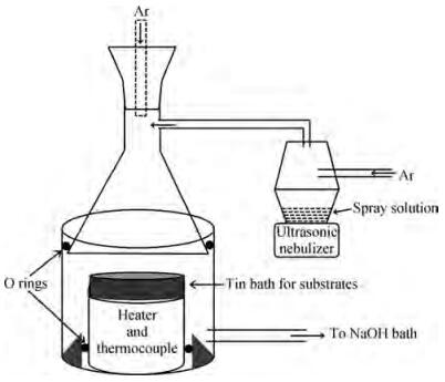
Fig. 1.
Setup for the ultrasonic spray pyrolysis deposition of SnSe and SnSe$_{2}$ thin films.
SEMICONDUCTOR MATERIALS
Jorge Sergio Narro-Rios, Manoj Ramachandran, Dalia Martínez-Escobar and Aarón Sánchez-Juárez
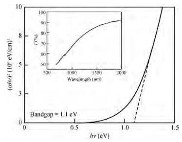
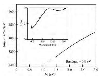
Abstract: Thin films of SnSe and SnSe2 have been deposited using the ultrasonic spray pyrolysis (USP) technique. To the best of our knowledge this is the first report of the deposition of SnSe and SnSe2 thin films using a single spray solution. The use of a single spray solution for obtaining both a p-type material, SnSe, and an n-type material, SnSe2, simplifies the deposition technique. The SnSe2 thin films have a bandgap of 1.1 eV and the SnSe thin films have a band gap of 0.9 eV. The Hall measurements were used to determine the resistivity of the thin films. The SnSe2 thin films show a resistivity of 36.73 Ω·cm and n-type conductivity while the SnSe thin films show a resistivity of 180 Ω·cm and p-type conductivity.
Keywords: SnSe, SnSe2, ultrasonic spray pyrolysis technique
| [1] |
Chung K M, Wamwangi D, Woda M, et al. Investigation of SnSe, SnSe2, and Sn2Se3 alloys for phase change memory applications. J Appl Phys, 2008, 103(8):083523 doi: 10.1063/1.2894903
|
| [2] |
Xue M Z, Yao J, Cheng S C, et al. Lithium electrochemistry of a novel SnSe thin-film anode. J Electrochem Soc, 2006, 153(2):270 doi: 10.1149/1.2139871
|
| [3] |
Palosz B, Salje E. Lattice parameters and spontaneous strain in AX2 polytypes Cdl2, Pbl2, SnS2 and SnSe2. J Appl Crystallogr, 1989, 22(6):622 doi: 10.1107/S0021889889006916
|
| [4] |
Kumar N, Sharma V, Padha N, et al. Influence of the substrate temperature on the structural, optical, and electrical properties of tin selenide thin films deposited by thermal evaporation method. Cryst Res Technology, 2010, 45(1):53 doi: 10.1002/crat.v45:1
|
| [5] |
Mathews N R. Electrodeposited tin selenide thin films for photovoltaic applications. Solar Energy, 2012, 86(4):1010 doi: 10.1016/j.solener.2011.06.012
|
| [6] |
Liang Y Q, Cui Z D, Zhu S L, et al. SnSe nanoparticles anchored on TiO2 nanotube arrays by pulsed electrochemical deposition. Electrochem Solid-State Lett, 2012, 15(1):D4 doi: 10.1149/2.003201esl
|
| [7] |
Murali K R, Ananthi K, Muthukumarasamy N, et al. Pulse plated SnSe films and their properties. 219th ECS Meeting, 2011, 1101:1550
|
| [8] |
Bicer M, Sisman I. Electrodeposition and growth mechanism of SnSe thin films. Appl Surf Sci, 2011, 257(7):2944 doi: 10.1016/j.apsusc.2010.10.096
|
| [9] |
Pawar S M, Pawar B S, Kim J H, et al. Recent status of chemical bath deposited metal chalcogenide and metal oxide thin films. Current Applied Physics, 2011, 11(2):117 doi: 10.1016/j.cap.2010.07.007
|
| [10] |
Popescu M, Sava F, Lorinczi A, et al. Structure, properties and gas sensing effect of SnSe2 films prepared by pulsed laser deposition method. Journal of Non-Crystalline Solids, 2007, 353(18-21):1865 doi: 10.1016/j.jnoncrysol.2007.02.055
|
| [11] |
Boscher N D, Carmat C J, Palgrave R G, et al. Atmospheric pressure chemical vapour deposition of SnSe and SnSe2 thin films on glass. Thin Solid Films, 2008, 516(15):4750 doi: 10.1016/j.tsf.2007.08.100
|
| [12] |
Mariappan R, Ragavendar M, Gowrisankar G. Growth and characterization of SnSe thin films prepared by spray pyrolysis technique. Chalcogenide Lett, 2010, 7(3):211
|
| [13] |
Demyanets L N, Kireev V V, Li L E, et al. Thin films of ZnO:M synthesized by ultrasonic spray pyrolysis. Russian Journal of Inorganic Chemistry, 2011, 56(10):1509 doi: 10.1134/S0036023611100056
|
| [14] |
Gullen C, Montero J, Herrero J. Characteristics of SnSe and SnSe2 thin films grown onto polycrystalline SnO2-coated glass substrates. Phys Status Solidi A, 2011, 208(3):679 doi: 10.1002/pssa.v208.3
|
| [15] |
Schluter M, Cohen M L. Valence-band density of states and chemical bonding for several non-transition-metal layer compounds SnSe2, PbI2, BiI3, and GaSe. Phys Rev B, 1976, 14(2):424 doi: 10.1103/PhysRevB.14.424
|
| [16] |
Waghmare U V, Spaldin N A, Kandpal H C, et al. First-principles indicators of metallicity and cation off-centricity in the Ⅳ-Ⅵ rocksalt chalcogenides of divalent Ge, Sn, and Pb. Phys Rev B, 2003, 67(12):125111 doi: 10.1103/PhysRevB.67.125111
|
| [17] |
Yu L M, Degiovanni A, Thiry P A, et al. Infrared optical constants of orthorhombic Ⅳ-Ⅵ lamellar semiconductors refined by a combined study using optical and electronic spectroscopies. Phys Rev B, 1993, 47(24):16222 doi: 10.1103/PhysRevB.47.16222
|
| [18] |
Schroder D K. Semiconductor material and device characterization. 2nd ed. New York:Wiley, 1998
|


Article views: 3438 Times PDF downloads: 37 Times Cited by: 0 Times
Received: 19 April 2012 Revised: 09 August 2012 Online: Published: 01 January 2013
| Citation: |
Jorge Sergio Narro-Rios, Manoj Ramachandran, Dalia Martínez-Escobar, Aarón Sánchez-Juárez. Ultrasonic spray pyrolysis deposition of SnSe and SnSe2 using a single spray solution[J]. Journal of Semiconductors, 2013, 34(1): 013001. doi: 10.1088/1674-4926/34/1/013001
****
J S Narro-Rios, M Ramachandran, D Martínez-Escobar, A Sánchez-Juárez. Ultrasonic spray pyrolysis deposition of SnSe and SnSe2 using a single spray solution[J]. J. Semicond., 2013, 34(1): 013001. doi: 10.1088/1674-4926/34/1/013001.

|
| [1] |
Chung K M, Wamwangi D, Woda M, et al. Investigation of SnSe, SnSe2, and Sn2Se3 alloys for phase change memory applications. J Appl Phys, 2008, 103(8):083523 doi: 10.1063/1.2894903
|
| [2] |
Xue M Z, Yao J, Cheng S C, et al. Lithium electrochemistry of a novel SnSe thin-film anode. J Electrochem Soc, 2006, 153(2):270 doi: 10.1149/1.2139871
|
| [3] |
Palosz B, Salje E. Lattice parameters and spontaneous strain in AX2 polytypes Cdl2, Pbl2, SnS2 and SnSe2. J Appl Crystallogr, 1989, 22(6):622 doi: 10.1107/S0021889889006916
|
| [4] |
Kumar N, Sharma V, Padha N, et al. Influence of the substrate temperature on the structural, optical, and electrical properties of tin selenide thin films deposited by thermal evaporation method. Cryst Res Technology, 2010, 45(1):53 doi: 10.1002/crat.v45:1
|
| [5] |
Mathews N R. Electrodeposited tin selenide thin films for photovoltaic applications. Solar Energy, 2012, 86(4):1010 doi: 10.1016/j.solener.2011.06.012
|
| [6] |
Liang Y Q, Cui Z D, Zhu S L, et al. SnSe nanoparticles anchored on TiO2 nanotube arrays by pulsed electrochemical deposition. Electrochem Solid-State Lett, 2012, 15(1):D4 doi: 10.1149/2.003201esl
|
| [7] |
Murali K R, Ananthi K, Muthukumarasamy N, et al. Pulse plated SnSe films and their properties. 219th ECS Meeting, 2011, 1101:1550
|
| [8] |
Bicer M, Sisman I. Electrodeposition and growth mechanism of SnSe thin films. Appl Surf Sci, 2011, 257(7):2944 doi: 10.1016/j.apsusc.2010.10.096
|
| [9] |
Pawar S M, Pawar B S, Kim J H, et al. Recent status of chemical bath deposited metal chalcogenide and metal oxide thin films. Current Applied Physics, 2011, 11(2):117 doi: 10.1016/j.cap.2010.07.007
|
| [10] |
Popescu M, Sava F, Lorinczi A, et al. Structure, properties and gas sensing effect of SnSe2 films prepared by pulsed laser deposition method. Journal of Non-Crystalline Solids, 2007, 353(18-21):1865 doi: 10.1016/j.jnoncrysol.2007.02.055
|
| [11] |
Boscher N D, Carmat C J, Palgrave R G, et al. Atmospheric pressure chemical vapour deposition of SnSe and SnSe2 thin films on glass. Thin Solid Films, 2008, 516(15):4750 doi: 10.1016/j.tsf.2007.08.100
|
| [12] |
Mariappan R, Ragavendar M, Gowrisankar G. Growth and characterization of SnSe thin films prepared by spray pyrolysis technique. Chalcogenide Lett, 2010, 7(3):211
|
| [13] |
Demyanets L N, Kireev V V, Li L E, et al. Thin films of ZnO:M synthesized by ultrasonic spray pyrolysis. Russian Journal of Inorganic Chemistry, 2011, 56(10):1509 doi: 10.1134/S0036023611100056
|
| [14] |
Gullen C, Montero J, Herrero J. Characteristics of SnSe and SnSe2 thin films grown onto polycrystalline SnO2-coated glass substrates. Phys Status Solidi A, 2011, 208(3):679 doi: 10.1002/pssa.v208.3
|
| [15] |
Schluter M, Cohen M L. Valence-band density of states and chemical bonding for several non-transition-metal layer compounds SnSe2, PbI2, BiI3, and GaSe. Phys Rev B, 1976, 14(2):424 doi: 10.1103/PhysRevB.14.424
|
| [16] |
Waghmare U V, Spaldin N A, Kandpal H C, et al. First-principles indicators of metallicity and cation off-centricity in the Ⅳ-Ⅵ rocksalt chalcogenides of divalent Ge, Sn, and Pb. Phys Rev B, 2003, 67(12):125111 doi: 10.1103/PhysRevB.67.125111
|
| [17] |
Yu L M, Degiovanni A, Thiry P A, et al. Infrared optical constants of orthorhombic Ⅳ-Ⅵ lamellar semiconductors refined by a combined study using optical and electronic spectroscopies. Phys Rev B, 1993, 47(24):16222 doi: 10.1103/PhysRevB.47.16222
|
| [18] |
Schroder D K. Semiconductor material and device characterization. 2nd ed. New York:Wiley, 1998
|

 WeChat ID
Journal of Semiconductors © 2017 All Rights Reserved 京ICP备05085259号-2

 DownLoad:

