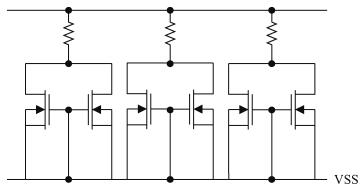
Fig. 1.
Circuit diagram of the multi-finger GG-nLDMOS.
SEMICONDUCTOR DEVICES
Chuan He, Lingli Jiang, Hang Fan and Bo Zhang
Corresponding author: He Chuan, Email:jack871107@163.com
Abstract: With the impact of the non-uniform turn-on phenomenon, the ESD robustness of high-voltage multi-finger devices is limited. This paper describes the operational mechanism of a GG-nLDMOS device under ESD stress conditions and analyzes the reason that causes the non-uniform turn-on characteristics of a multi-finger GG-nLDMOS device. By means of increasing substrate resistance, an optimized device structure is proposed to improve the turn-on uniformity of a high-voltage multi-finger GG-nLDMOS. This approach has been successfully verified in a 0.35 μm 40 V BCD process. The TLP test results reveal that increasing the substrate resistance can effectively enhance the turn-on uniformity of the 40 V multi-finger GG-nLDMOS device and improve its ESD robustness.
Keywords: ESD, multi-finger, GGLDMOS, turn-on uniformity
| [1] |
Chun J, Nowak E, Manley M. Process and design for ESD robustness in deep submicron CMOS technology. IEEE International Reliability Physics Symposium, 1996: 233
|
| [2] |
Oh K H, Duvvury C, Banerjee K, et al. Analysis of nonuniform ESD current distribution in deep submicron NMOS transistors. IEEE Trans Electron Devices, 2002, 49(12):2171 doi: 10.1109/TED.2002.805049
|
| [3] |
Chen T Y, Ker M D. Investigation of the gate-driven effect and substrate-triggered effect on ESD robustness of CMOS devices. IEEE Trans Device Mater Reliab, 2001, 1(4):190 doi: 10.1109/7298.995833
|
| [4] |
Russ C, Bock K, Rasras M, et al. Non-uniform triggering of gg-nMOSt investigated by combined emission microscopy and transmission line pulsing. Electrical Overstress/Electrostatic Discharge Symposium Proceedings, 1998: 177
|
| [5] |
Lee J H, Wu Y H, Tang C H, et al. A simple and useful layout scheme to achieve uniform current distribution for multi-finger silicided grounded-gate NMOS. IEEE International Reliability Physics Symposium, 2007: 588
|
| [6] |
Ker M D, Chen T Y. Substrate-triggered technique for on-chip ESD protection design in a 0.18μm salicided CMOS process. IEEE Trans Electron Devices, 2003, 50(2):1050
|
| [7] |
Polgreen T L, Chatterjee A. Improving the ESD failure threshold of silicided n-MOS output transistors by ensuring uniform current flow. IEEE Trans Electron Devices, 1992, 39(2):379 doi: 10.1109/16.121697
|
| [8] |
Fujiwara S, Nakaya K, Hirano T, et al. Source engineering for ESD robust NLDMOS. Electrical Overstress/Electrostatic Discharge Symposium Proceedings, 2011: 1
|
Table 1. TLP test results of the conventional and optimized 40 V GG-nLDMOS.

|
| [1] |
Chun J, Nowak E, Manley M. Process and design for ESD robustness in deep submicron CMOS technology. IEEE International Reliability Physics Symposium, 1996: 233
|
| [2] |
Oh K H, Duvvury C, Banerjee K, et al. Analysis of nonuniform ESD current distribution in deep submicron NMOS transistors. IEEE Trans Electron Devices, 2002, 49(12):2171 doi: 10.1109/TED.2002.805049
|
| [3] |
Chen T Y, Ker M D. Investigation of the gate-driven effect and substrate-triggered effect on ESD robustness of CMOS devices. IEEE Trans Device Mater Reliab, 2001, 1(4):190 doi: 10.1109/7298.995833
|
| [4] |
Russ C, Bock K, Rasras M, et al. Non-uniform triggering of gg-nMOSt investigated by combined emission microscopy and transmission line pulsing. Electrical Overstress/Electrostatic Discharge Symposium Proceedings, 1998: 177
|
| [5] |
Lee J H, Wu Y H, Tang C H, et al. A simple and useful layout scheme to achieve uniform current distribution for multi-finger silicided grounded-gate NMOS. IEEE International Reliability Physics Symposium, 2007: 588
|
| [6] |
Ker M D, Chen T Y. Substrate-triggered technique for on-chip ESD protection design in a 0.18μm salicided CMOS process. IEEE Trans Electron Devices, 2003, 50(2):1050
|
| [7] |
Polgreen T L, Chatterjee A. Improving the ESD failure threshold of silicided n-MOS output transistors by ensuring uniform current flow. IEEE Trans Electron Devices, 1992, 39(2):379 doi: 10.1109/16.121697
|
| [8] |
Fujiwara S, Nakaya K, Hirano T, et al. Source engineering for ESD robust NLDMOS. Electrical Overstress/Electrostatic Discharge Symposium Proceedings, 2011: 1
|


Article views: 2948 Times PDF downloads: 54 Times Cited by: 0 Times
Received: 01 June 2012 Revised: 06 August 2012 Online: Published: 01 January 2013
| Citation: |
Chuan He, Lingli Jiang, Hang Fan, Bo Zhang. Increasing substrate resistance to improve the turn-on uniformity of a high-voltage multi-finger GG-nLDMOS[J]. Journal of Semiconductors, 2013, 34(1): 014006. doi: 10.1088/1674-4926/34/1/014006
****
C He, L L Jiang, H Fan, B Zhang. Increasing substrate resistance to improve the turn-on uniformity of a high-voltage multi-finger GG-nLDMOS[J]. J. Semicond., 2013, 34(1): 014006. doi: 10.1088/1674-4926/34/1/014006.

|
| [1] |
Chun J, Nowak E, Manley M. Process and design for ESD robustness in deep submicron CMOS technology. IEEE International Reliability Physics Symposium, 1996: 233
|
| [2] |
Oh K H, Duvvury C, Banerjee K, et al. Analysis of nonuniform ESD current distribution in deep submicron NMOS transistors. IEEE Trans Electron Devices, 2002, 49(12):2171 doi: 10.1109/TED.2002.805049
|
| [3] |
Chen T Y, Ker M D. Investigation of the gate-driven effect and substrate-triggered effect on ESD robustness of CMOS devices. IEEE Trans Device Mater Reliab, 2001, 1(4):190 doi: 10.1109/7298.995833
|
| [4] |
Russ C, Bock K, Rasras M, et al. Non-uniform triggering of gg-nMOSt investigated by combined emission microscopy and transmission line pulsing. Electrical Overstress/Electrostatic Discharge Symposium Proceedings, 1998: 177
|
| [5] |
Lee J H, Wu Y H, Tang C H, et al. A simple and useful layout scheme to achieve uniform current distribution for multi-finger silicided grounded-gate NMOS. IEEE International Reliability Physics Symposium, 2007: 588
|
| [6] |
Ker M D, Chen T Y. Substrate-triggered technique for on-chip ESD protection design in a 0.18μm salicided CMOS process. IEEE Trans Electron Devices, 2003, 50(2):1050
|
| [7] |
Polgreen T L, Chatterjee A. Improving the ESD failure threshold of silicided n-MOS output transistors by ensuring uniform current flow. IEEE Trans Electron Devices, 1992, 39(2):379 doi: 10.1109/16.121697
|
| [8] |
Fujiwara S, Nakaya K, Hirano T, et al. Source engineering for ESD robust NLDMOS. Electrical Overstress/Electrostatic Discharge Symposium Proceedings, 2011: 1
|

 WeChat ID
Journal of Semiconductors © 2017 All Rights Reserved 京ICP备05085259号-2

 DownLoad: