


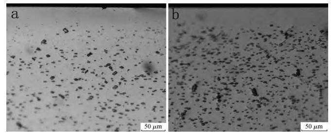
Fig. 1.
OM images of the BMDs' distribution in the samples (a) A1 and (b) M1
SEMICONDUCTOR MATERIALS
Chuan Ji1, Guangchao Zhang1 and Jin Xu1, 2,
Corresponding author: Xu Jin, xujinmse@xmu.edu.cn
Abstract: The influence of co-precipitation of copper and nickel on the formation of a denuded zone (DZ) in Czochralski silicon (Cz Si) was systematically investigated by means of etching and optical microscopy (OM). It was found that, for conventional high-low-high annealing (CFA), the DZ could be obtained in all specimens contaminated by copper and nickel co-impurity at different steps of the heat treatment, indicating that no copper precipitates or nickel precipitates were generated in the region just below the surface. However, for rapid thermal annealing (RTA)-low-high annealing, the tendency is not the same; the DZ could not be found in the specimen which was contaminated by copper and nickel contamination before the first RTA annealing. On the basis of the experimental results, it was supposed that the concentration and distribution of the vacancies generating during the RTA can influence the distribution of copper precipitation and nickel precipitation along the cross-section of Cz Si significantly, and thus influence the formation of the DZ to a great extent.
Keywords: Czochralski silicon, co-precipitation, denuded zone
| [1] |
Istratov A A, Weber E R. Physics of copper in silicon. J Electrochem Soc, 2002, 149(1):G21 doi: 10.1149/1.1421348
|
| [2] |
Weber E R. Transition metals in silicon. Appl Phys A, 1983, 30:1 doi: 10.1007/BF00617708
|
| [3] |
Bokhonov B, Korchagin M. In-situ investigation of the formation of nickel silicides during interaction of single-crystalline and amorphous silicon with nickel. Journal of Alloys and Compounds, 2001, 319:187 doi: 10.1016/S0925-8388(01)00902-1
|
| [4] |
Xu J, Yang D R, Moeller H J. Influence of copper precipitation on the formation of denuded zone in Czochralski silicon. J Appl Phys, 2007, 102:114506 doi: 10.1063/1.2821311
|
| [5] |
Xu J, Wang Y Z, Yang D R, et al. Influence of nickel precipitation on the formation of denuded zone in Czochralski silicon. Journal of Alloys and Compounds, 2010, 502:351 doi: 10.1016/j.jallcom.2010.04.164
|
| [6] |
Myers S M, Seibt M, Schröter W. Mechanisms of transition-metal gettering in silicon. J Appl Phys, 2000, 88(7):3795 doi: 10.1063/1.1289273
|
| [7] |
Istratov A A, Weber E R. Electrical properties and recombination activity of copper, nickel and cobalt in silicon. Appl Phys A:Mater Sci Processing, 1998, 66:123 doi: 10.1007/s003390050649
|
| [8] |
Rizk R, Portier X, Allais G, et al. Electrical and structural studies of copper and nickel precipitates in a Σ=25 silicon bicrystal. J Appl Phys, 1994, 76:952 doi: 10.1063/1.357773
|
| [9] |
Palais O, Yakimov E, Martinuzzi S. Minority carrier lifetime scan maps applied to iron concentration mapping in silicon wafers. Mater Sci Eng B, 2002, 91:216 http://www.sciencedirect.com/science/article/pii/S0921510701009989
|
| [10] |
Buonassisi T, Heuer M, Istratov A A. Transition metal co-precipitation mechanisms in silicon. Acta Materialia, 2007, 55:6119 doi: 10.1016/j.actamat.2007.07.030
|
| [11] |
Saring P, Rudolf C, Stolze L, et al. Light-beam-induced current measurements on copper-nickel co-contaminated Cz-silicon bicrystals. Mater Sci Eng B, 2009, 159/160:216 doi: 10.1016/j.mseb.2008.10.046
|
| [12] |
Falster R, Voronkov V V. The engineering of intrinsic point defects in silicon wafers and crystals. Mater Sci Eng B, 2000, 73(1-3):87 doi: 10.1016/S0921-5107(99)00439-0
|
| [13] |
Tan T Y, Gardner E E, Tice W K. Intrinsic gettering by oxide precipitate induced dislocations in Czochralski Si. Appl Phys Lett, 1977, 30:175 doi: 10.1063/1.89340
|
| [14] |
Xi Z Q, Chen J, Yang D R. Copper precipitation in large-diameter Czochralski silicon. J Appl Phys, 2005, 97:094909 doi: 10.1063/1.1875740
|
| [15] |
Rozgonyi G A, Pearce C W. Gettering of surface and bulk impurities in Czochralski silicon wafers. Appl Phys Lett, 1978, 32(11):747 doi: 10.1063/1.89908
|
| [16] |
Yu X G, Ma X Y, Yang D R. Rapid thermal process of large diameter Czochralski silicon. Chinese Journal of Semiconductors, 2003, 24(5):491 http://en.cnki.com.cn/Article_en/CJFDTOTAL-BDTX200305008.htm
|
| [17] |
Falster R, Voronkov V V, Quast F. On the Properties of the intrinsic point defects in silicon:a perspective from crystal growth and wafer processing. Phys Status Solidi B, 2000, 222:219 doi: 10.1002/(ISSN)1521-3951
|
| [18] |
Pagani M, Falster R J, Fisher G R, et al. Spatial variations in oxygen precipitation in silicon after high temperature rapid thermal annealing. Appl Phys Lett, 1997, 70:1572 doi: 10.1063/1.118620
|
| [19] |
Xi Z Q, Yang D R, Chen J, et al. Investigation of copper precipitation in as-grown Czochralski silicon. Chinese Journal of Semiconductors, 2005, 26(9):1754 http://www.oalib.com/paper/1518316
|
| [20] |
Xi Z Q, Yang D R, Jin X, et al. Effect of intrinsic point defects on copper precipitation in large-diameter Czochralski silicon. Appl Phys Lett, 2003, 83(15):3048 doi: 10.1063/1.1617377
|
| [21] |
Shabani M B, Yoshimi T, Okuuchi S, et al. A quantitative method of metal impurities depth profiling for gettering evaluation in silicon wafers. Solid State Phenomena, 1997, 57:81 https://www.scientific.net/SSP.57-58.103.pdf
|
| [22] |
Heuer M, Buonassisi T, Marcus M A, et al. Complex intermetallic phase in multicrystalline silicon doped with transition metals. Phys Rev B, 2006, 73:235204 doi: 10.1103/PhysRevB.73.235204
|
| [23] |
Istratov A A, Flink C, Hieslmair H, et al. Intrinsic diffusion coefficient of interstitial copper in silicon. Phys Rev Lett, 1998, 81:1243 doi: 10.1103/PhysRevLett.81.1243
|
| [24] |
McHugo S G, Mohammed A, Thompson A C, et al. Copper precipitates in silicon:precipitation, dissolution, and chemical state. J Appl Phys, 2002, 91(10):6396 doi: 10.1063/1.1471944
|
| [25] |
Xi Z Q, Yang D R, Chen J, et al. Nickel precipitation in large-diameter Czochralski silicon. Phys B:Condensed Matter, 2004, 344(1-4):407 doi: 10.1016/j.physb.2003.10.020
|
| [26] |
Török P, Mule'stagno L. Applications of scanning optical microscopy in materials science to detect bulk microdefects in semiconductors. Journal of Microscopy, 1997, 188:1 doi: 10.1046/j.1365-2818.1997.2420800.x
|
| [27] |
Booker G R, Laczik Z, Kidd P. The scanning infrared microscopy (SIRM) and its application to bulk GaAs and Si:a review. Semicond Sci Technol, 1992, 7:A110 doi: 10.1088/0268-1242/7/1A/021
|
| [28] |
Borghesi A, Pivac B, Sassella A, et al. Oxygen precipitation in silicon. J Appl Phys, 1995, 77:4196 doi: 10.1007/978-4-431-55800-2_6
|
| [29] |
Gay N, Martinuzzi S. External self-gettering of nickel in float zone silicon wafers. Appl Phys Lett, 1997, 70:2568 doi: 10.1063/1.118921
|
| [30] |
Cui C, Yang D R, Ma X Y. Effects of annealing atmosphere on bulk micro-defects in czochralski silicon wafer. Chinese Journal of Semiconductors, 2007, 28(6):866 http://www.oalib.com/paper/1521475
|
| [31] |
Rudolf C, Saring P, Stolze L, et al. Co-precipitation of copper and nickel in crystalline silicon. Mater Sci Eng B, 2009, 159/160:365 doi: 10.1016/j.mseb.2008.10.015
|
Table 1. Annealing sequence and nickel contamination process
 |
| [1] |
Istratov A A, Weber E R. Physics of copper in silicon. J Electrochem Soc, 2002, 149(1):G21 doi: 10.1149/1.1421348
|
| [2] |
Weber E R. Transition metals in silicon. Appl Phys A, 1983, 30:1 doi: 10.1007/BF00617708
|
| [3] |
Bokhonov B, Korchagin M. In-situ investigation of the formation of nickel silicides during interaction of single-crystalline and amorphous silicon with nickel. Journal of Alloys and Compounds, 2001, 319:187 doi: 10.1016/S0925-8388(01)00902-1
|
| [4] |
Xu J, Yang D R, Moeller H J. Influence of copper precipitation on the formation of denuded zone in Czochralski silicon. J Appl Phys, 2007, 102:114506 doi: 10.1063/1.2821311
|
| [5] |
Xu J, Wang Y Z, Yang D R, et al. Influence of nickel precipitation on the formation of denuded zone in Czochralski silicon. Journal of Alloys and Compounds, 2010, 502:351 doi: 10.1016/j.jallcom.2010.04.164
|
| [6] |
Myers S M, Seibt M, Schröter W. Mechanisms of transition-metal gettering in silicon. J Appl Phys, 2000, 88(7):3795 doi: 10.1063/1.1289273
|
| [7] |
Istratov A A, Weber E R. Electrical properties and recombination activity of copper, nickel and cobalt in silicon. Appl Phys A:Mater Sci Processing, 1998, 66:123 doi: 10.1007/s003390050649
|
| [8] |
Rizk R, Portier X, Allais G, et al. Electrical and structural studies of copper and nickel precipitates in a Σ=25 silicon bicrystal. J Appl Phys, 1994, 76:952 doi: 10.1063/1.357773
|
| [9] |
Palais O, Yakimov E, Martinuzzi S. Minority carrier lifetime scan maps applied to iron concentration mapping in silicon wafers. Mater Sci Eng B, 2002, 91:216 http://www.sciencedirect.com/science/article/pii/S0921510701009989
|
| [10] |
Buonassisi T, Heuer M, Istratov A A. Transition metal co-precipitation mechanisms in silicon. Acta Materialia, 2007, 55:6119 doi: 10.1016/j.actamat.2007.07.030
|
| [11] |
Saring P, Rudolf C, Stolze L, et al. Light-beam-induced current measurements on copper-nickel co-contaminated Cz-silicon bicrystals. Mater Sci Eng B, 2009, 159/160:216 doi: 10.1016/j.mseb.2008.10.046
|
| [12] |
Falster R, Voronkov V V. The engineering of intrinsic point defects in silicon wafers and crystals. Mater Sci Eng B, 2000, 73(1-3):87 doi: 10.1016/S0921-5107(99)00439-0
|
| [13] |
Tan T Y, Gardner E E, Tice W K. Intrinsic gettering by oxide precipitate induced dislocations in Czochralski Si. Appl Phys Lett, 1977, 30:175 doi: 10.1063/1.89340
|
| [14] |
Xi Z Q, Chen J, Yang D R. Copper precipitation in large-diameter Czochralski silicon. J Appl Phys, 2005, 97:094909 doi: 10.1063/1.1875740
|
| [15] |
Rozgonyi G A, Pearce C W. Gettering of surface and bulk impurities in Czochralski silicon wafers. Appl Phys Lett, 1978, 32(11):747 doi: 10.1063/1.89908
|
| [16] |
Yu X G, Ma X Y, Yang D R. Rapid thermal process of large diameter Czochralski silicon. Chinese Journal of Semiconductors, 2003, 24(5):491 http://en.cnki.com.cn/Article_en/CJFDTOTAL-BDTX200305008.htm
|
| [17] |
Falster R, Voronkov V V, Quast F. On the Properties of the intrinsic point defects in silicon:a perspective from crystal growth and wafer processing. Phys Status Solidi B, 2000, 222:219 doi: 10.1002/(ISSN)1521-3951
|
| [18] |
Pagani M, Falster R J, Fisher G R, et al. Spatial variations in oxygen precipitation in silicon after high temperature rapid thermal annealing. Appl Phys Lett, 1997, 70:1572 doi: 10.1063/1.118620
|
| [19] |
Xi Z Q, Yang D R, Chen J, et al. Investigation of copper precipitation in as-grown Czochralski silicon. Chinese Journal of Semiconductors, 2005, 26(9):1754 http://www.oalib.com/paper/1518316
|
| [20] |
Xi Z Q, Yang D R, Jin X, et al. Effect of intrinsic point defects on copper precipitation in large-diameter Czochralski silicon. Appl Phys Lett, 2003, 83(15):3048 doi: 10.1063/1.1617377
|
| [21] |
Shabani M B, Yoshimi T, Okuuchi S, et al. A quantitative method of metal impurities depth profiling for gettering evaluation in silicon wafers. Solid State Phenomena, 1997, 57:81 https://www.scientific.net/SSP.57-58.103.pdf
|
| [22] |
Heuer M, Buonassisi T, Marcus M A, et al. Complex intermetallic phase in multicrystalline silicon doped with transition metals. Phys Rev B, 2006, 73:235204 doi: 10.1103/PhysRevB.73.235204
|
| [23] |
Istratov A A, Flink C, Hieslmair H, et al. Intrinsic diffusion coefficient of interstitial copper in silicon. Phys Rev Lett, 1998, 81:1243 doi: 10.1103/PhysRevLett.81.1243
|
| [24] |
McHugo S G, Mohammed A, Thompson A C, et al. Copper precipitates in silicon:precipitation, dissolution, and chemical state. J Appl Phys, 2002, 91(10):6396 doi: 10.1063/1.1471944
|
| [25] |
Xi Z Q, Yang D R, Chen J, et al. Nickel precipitation in large-diameter Czochralski silicon. Phys B:Condensed Matter, 2004, 344(1-4):407 doi: 10.1016/j.physb.2003.10.020
|
| [26] |
Török P, Mule'stagno L. Applications of scanning optical microscopy in materials science to detect bulk microdefects in semiconductors. Journal of Microscopy, 1997, 188:1 doi: 10.1046/j.1365-2818.1997.2420800.x
|
| [27] |
Booker G R, Laczik Z, Kidd P. The scanning infrared microscopy (SIRM) and its application to bulk GaAs and Si:a review. Semicond Sci Technol, 1992, 7:A110 doi: 10.1088/0268-1242/7/1A/021
|
| [28] |
Borghesi A, Pivac B, Sassella A, et al. Oxygen precipitation in silicon. J Appl Phys, 1995, 77:4196 doi: 10.1007/978-4-431-55800-2_6
|
| [29] |
Gay N, Martinuzzi S. External self-gettering of nickel in float zone silicon wafers. Appl Phys Lett, 1997, 70:2568 doi: 10.1063/1.118921
|
| [30] |
Cui C, Yang D R, Ma X Y. Effects of annealing atmosphere on bulk micro-defects in czochralski silicon wafer. Chinese Journal of Semiconductors, 2007, 28(6):866 http://www.oalib.com/paper/1521475
|
| [31] |
Rudolf C, Saring P, Stolze L, et al. Co-precipitation of copper and nickel in crystalline silicon. Mater Sci Eng B, 2009, 159/160:365 doi: 10.1016/j.mseb.2008.10.015
|


Article views: 2918 Times PDF downloads: 16 Times Cited by: 0 Times
Received: 11 December 2012 Revised: 07 April 2013 Online: Published: 01 October 2013
| Citation: |
Chuan Ji, Guangchao Zhang, Jin Xu. Influence of co-precipitation of copper and nickel on the formation of a denuded zone in Czochralski silicon[J]. Journal of Semiconductors, 2013, 34(10): 103005. doi: 10.1088/1674-4926/34/10/103005
****
C Ji, G C Zhang, J Xu. Influence of co-precipitation of copper and nickel on the formation of a denuded zone in Czochralski silicon[J]. J. Semicond., 2013, 34(10): 103005. doi: 10.1088/1674-4926/34/10/103005.

|
| [1] |
Istratov A A, Weber E R. Physics of copper in silicon. J Electrochem Soc, 2002, 149(1):G21 doi: 10.1149/1.1421348
|
| [2] |
Weber E R. Transition metals in silicon. Appl Phys A, 1983, 30:1 doi: 10.1007/BF00617708
|
| [3] |
Bokhonov B, Korchagin M. In-situ investigation of the formation of nickel silicides during interaction of single-crystalline and amorphous silicon with nickel. Journal of Alloys and Compounds, 2001, 319:187 doi: 10.1016/S0925-8388(01)00902-1
|
| [4] |
Xu J, Yang D R, Moeller H J. Influence of copper precipitation on the formation of denuded zone in Czochralski silicon. J Appl Phys, 2007, 102:114506 doi: 10.1063/1.2821311
|
| [5] |
Xu J, Wang Y Z, Yang D R, et al. Influence of nickel precipitation on the formation of denuded zone in Czochralski silicon. Journal of Alloys and Compounds, 2010, 502:351 doi: 10.1016/j.jallcom.2010.04.164
|
| [6] |
Myers S M, Seibt M, Schröter W. Mechanisms of transition-metal gettering in silicon. J Appl Phys, 2000, 88(7):3795 doi: 10.1063/1.1289273
|
| [7] |
Istratov A A, Weber E R. Electrical properties and recombination activity of copper, nickel and cobalt in silicon. Appl Phys A:Mater Sci Processing, 1998, 66:123 doi: 10.1007/s003390050649
|
| [8] |
Rizk R, Portier X, Allais G, et al. Electrical and structural studies of copper and nickel precipitates in a Σ=25 silicon bicrystal. J Appl Phys, 1994, 76:952 doi: 10.1063/1.357773
|
| [9] |
Palais O, Yakimov E, Martinuzzi S. Minority carrier lifetime scan maps applied to iron concentration mapping in silicon wafers. Mater Sci Eng B, 2002, 91:216 http://www.sciencedirect.com/science/article/pii/S0921510701009989
|
| [10] |
Buonassisi T, Heuer M, Istratov A A. Transition metal co-precipitation mechanisms in silicon. Acta Materialia, 2007, 55:6119 doi: 10.1016/j.actamat.2007.07.030
|
| [11] |
Saring P, Rudolf C, Stolze L, et al. Light-beam-induced current measurements on copper-nickel co-contaminated Cz-silicon bicrystals. Mater Sci Eng B, 2009, 159/160:216 doi: 10.1016/j.mseb.2008.10.046
|
| [12] |
Falster R, Voronkov V V. The engineering of intrinsic point defects in silicon wafers and crystals. Mater Sci Eng B, 2000, 73(1-3):87 doi: 10.1016/S0921-5107(99)00439-0
|
| [13] |
Tan T Y, Gardner E E, Tice W K. Intrinsic gettering by oxide precipitate induced dislocations in Czochralski Si. Appl Phys Lett, 1977, 30:175 doi: 10.1063/1.89340
|
| [14] |
Xi Z Q, Chen J, Yang D R. Copper precipitation in large-diameter Czochralski silicon. J Appl Phys, 2005, 97:094909 doi: 10.1063/1.1875740
|
| [15] |
Rozgonyi G A, Pearce C W. Gettering of surface and bulk impurities in Czochralski silicon wafers. Appl Phys Lett, 1978, 32(11):747 doi: 10.1063/1.89908
|
| [16] |
Yu X G, Ma X Y, Yang D R. Rapid thermal process of large diameter Czochralski silicon. Chinese Journal of Semiconductors, 2003, 24(5):491 http://en.cnki.com.cn/Article_en/CJFDTOTAL-BDTX200305008.htm
|
| [17] |
Falster R, Voronkov V V, Quast F. On the Properties of the intrinsic point defects in silicon:a perspective from crystal growth and wafer processing. Phys Status Solidi B, 2000, 222:219 doi: 10.1002/(ISSN)1521-3951
|
| [18] |
Pagani M, Falster R J, Fisher G R, et al. Spatial variations in oxygen precipitation in silicon after high temperature rapid thermal annealing. Appl Phys Lett, 1997, 70:1572 doi: 10.1063/1.118620
|
| [19] |
Xi Z Q, Yang D R, Chen J, et al. Investigation of copper precipitation in as-grown Czochralski silicon. Chinese Journal of Semiconductors, 2005, 26(9):1754 http://www.oalib.com/paper/1518316
|
| [20] |
Xi Z Q, Yang D R, Jin X, et al. Effect of intrinsic point defects on copper precipitation in large-diameter Czochralski silicon. Appl Phys Lett, 2003, 83(15):3048 doi: 10.1063/1.1617377
|
| [21] |
Shabani M B, Yoshimi T, Okuuchi S, et al. A quantitative method of metal impurities depth profiling for gettering evaluation in silicon wafers. Solid State Phenomena, 1997, 57:81 https://www.scientific.net/SSP.57-58.103.pdf
|
| [22] |
Heuer M, Buonassisi T, Marcus M A, et al. Complex intermetallic phase in multicrystalline silicon doped with transition metals. Phys Rev B, 2006, 73:235204 doi: 10.1103/PhysRevB.73.235204
|
| [23] |
Istratov A A, Flink C, Hieslmair H, et al. Intrinsic diffusion coefficient of interstitial copper in silicon. Phys Rev Lett, 1998, 81:1243 doi: 10.1103/PhysRevLett.81.1243
|
| [24] |
McHugo S G, Mohammed A, Thompson A C, et al. Copper precipitates in silicon:precipitation, dissolution, and chemical state. J Appl Phys, 2002, 91(10):6396 doi: 10.1063/1.1471944
|
| [25] |
Xi Z Q, Yang D R, Chen J, et al. Nickel precipitation in large-diameter Czochralski silicon. Phys B:Condensed Matter, 2004, 344(1-4):407 doi: 10.1016/j.physb.2003.10.020
|
| [26] |
Török P, Mule'stagno L. Applications of scanning optical microscopy in materials science to detect bulk microdefects in semiconductors. Journal of Microscopy, 1997, 188:1 doi: 10.1046/j.1365-2818.1997.2420800.x
|
| [27] |
Booker G R, Laczik Z, Kidd P. The scanning infrared microscopy (SIRM) and its application to bulk GaAs and Si:a review. Semicond Sci Technol, 1992, 7:A110 doi: 10.1088/0268-1242/7/1A/021
|
| [28] |
Borghesi A, Pivac B, Sassella A, et al. Oxygen precipitation in silicon. J Appl Phys, 1995, 77:4196 doi: 10.1007/978-4-431-55800-2_6
|
| [29] |
Gay N, Martinuzzi S. External self-gettering of nickel in float zone silicon wafers. Appl Phys Lett, 1997, 70:2568 doi: 10.1063/1.118921
|
| [30] |
Cui C, Yang D R, Ma X Y. Effects of annealing atmosphere on bulk micro-defects in czochralski silicon wafer. Chinese Journal of Semiconductors, 2007, 28(6):866 http://www.oalib.com/paper/1521475
|
| [31] |
Rudolf C, Saring P, Stolze L, et al. Co-precipitation of copper and nickel in crystalline silicon. Mater Sci Eng B, 2009, 159/160:365 doi: 10.1016/j.mseb.2008.10.015
|

 WeChat ID
Journal of Semiconductors © 2017 All Rights Reserved 京ICP备05085259号-2

 DownLoad:

