


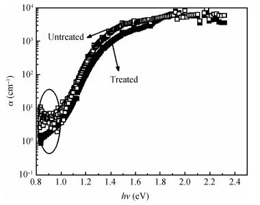
Fig. 1.
Absorption coefficient of samples deposited with and without hydrogen plasma treatment
SEMICONDUCTOR MATERIALS
Jingyan Li, Xiangbo Zeng, Hao Li, Xiaobing Xie, Ping Yang, Haibo Xiao, Xiaodong Zhang and Qiming Wang
Corresponding author: Zeng Xiangbo, xbzeng@semi.ac.cn
Abstract: The effect of hydrogen plasma treatment (HPT) during the initial stage of microcrystalline silicon (μc-Si) growth on the defect density of μc-Si has been investigated. Lower absorption coefficient in the 0.8-1.0 eV indicated less defect density compared to its counterpart without HPT. The infrared spectroscopy of μc-Si with HPT shows an increase in 2040 cm-1, which reveals more Si-H in the amorphous/crystalline interfaces. We ascribe the decrease of defect density to hydrogen passivation of the dangling bonds. Improved performance of μc-Si solar cell with HPT is due to the reduced defect density.
Keywords: microcrystalline silicon, defect density, hydrogen plasma treatment, passivation
| [1] |
Klein S, Finger F, Carius R. Intrinsic microcrystalline silicon prepared by hot-wire chemical vapour deposition for thin film solar cells. Thin Solid Films, 2003, 430(1/2):202 http://www.sciencedirect.com/science/article/pii/S0040609003001111
|
| [2] |
Bugnon G, Feltrin A, Meillaud F. Influence of pressure and silane depletion on microcrystalline silicon material quality and solar cell performance. J Appl Phys, 2009, 105(6):064507 doi: 10.1063/1.3095488
|
| [3] |
Poortmans J, Vladimir. Thin film solar cells fabrication, characterization and applications. England: John Wiley & Sons, 2006
|
| [4] |
Smets A H M, Matsui T, Kondo M. High-rate deposition of microcrystalline silicon p-i-n solar cells in the high pressure depletion regime. J Appl Phys, 2008, 104(3):034508 doi: 10.1063/1.2961334
|
| [5] |
Chen Y S, Wang J H. The effect of transient depletion of source gases on the properties of microcrystalline silicon solar cells. Sol Energy, 2009, 83(9):1454 doi: 10.1016/j.solener.2009.03.015
|
| [6] |
Ide Y, Saito Y, Yamada A, et al. 2-step growth method and microcrystalline silicon thin film solar cells prepared by hot wire cell method. Jpn J Appl Phys, 2004, 43(5A):2419 doi: 10.1143/JJAP.43.2419
|
| [7] |
Chantana J, Tsutsui Y, Sobajima Y. Importance of starting procedure for film growth in substrate-type microcrystalline-silicon solar cells. Jpn J Appl Phys, 2011, 50(4):045806 doi: 10.1143/JJAP.50.045806
|
| [8] |
Ihara H, Nozaki H. Improvement of hydrogenated amorphous silicon n-i-p diode performance by H2 plasma treatment for i/p interface. Jpn J Appl Phys, 1990, 29(12):2159 http://www.academia.edu/1811567/Amorphous_Silicon_Nanocone_Array_Solar_Cell
|
| [9] |
Ambrico M, Schiavulli L, Ligonzo T. Optical absorption and electrical conductivity measurements of microcrystalline silicon layers grown by SiF4/H plasma on glass substrates. Thin Solid Films, 2001, 383(1/2):200 http://www.academia.edu/14105049/Optical_absorption_and_electrical_conductivity_measurements_of_microcrystalline_silicon_layers_grown_by_SiF_rH_plasma_on_glass_4_2
|
| [10] |
Langford A A, Fleet M L, Nelson B P. Infrared absorption strength and hydrogen content of hydrogenated amorphous silicon. Phys Rev B, 1992, 45(23):13367 doi: 10.1103/PhysRevB.45.13367
|
| [11] |
Kaneko T, Wakagi M, Onisawa K. Change in crystalline morphologies of polycrystalline silicon films prepared by radiofrequency plasmaenhanced chemical vapor deposition using SiF4 + H2 gas mixture at 350℃. Appl Phys Lett, 1994, 64(14):1865 doi: 10.1063/1.111781
|
| [12] |
Han D, Wang K, Owens J M. Hydrogen structures and the optoelectronic properties in transition films from amorphous to microcrystalline silicon prepared by hot-wire chemical vapor deposition. J Appl Phys, 2003, 93(7):3776 doi: 10.1063/1.1555680
|
| [13] |
Bronneberg A C, Cankoy N, Sanden M C M. Ion-induced effects on grain boundaries and a-Si:H tissue quality in microcrystalline silicon films. J Vac Sci Technol A, 2012, 30(6):061512 doi: 10.1116/1.4766193
|
| [14] |
Keudell A V, Abelson J R. The interaction of atomic hydrogen with very thin amorphous hydrogenated silicon films analyzed using in situ real time infrared spectroscopy:reaction rates and the formation of hydrogen platelets. J Appl Phys, 1998, 84(1):489 doi: 10.1063/1.368082
|
| [15] |
Marra D C, Edelberg E A, Naone R L. Silicon hydride composition of plasma-deposited hydrogenated amorphous and nanocrystalline silicon films and surfaces. J Vac Sci Technol A, 1998, 16(6):3199 doi: 10.1116/1.581520
|
| [16] |
Xu L, Li Z P, Wen C. Bonded hydrogen in nanocrystalline silicon photovoltaic materials:impact on structure and defect density. J Appl Phys, 2011, 110(6):064315 doi: 10.1063/1.3638712
|
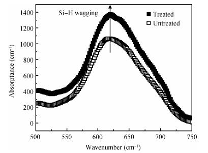
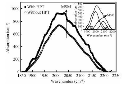
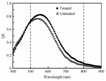
Table 1.
Experimental results of
 |
Table 2. Experimental results of solar cells deposited with and without HPT
 |
| [1] |
Klein S, Finger F, Carius R. Intrinsic microcrystalline silicon prepared by hot-wire chemical vapour deposition for thin film solar cells. Thin Solid Films, 2003, 430(1/2):202 http://www.sciencedirect.com/science/article/pii/S0040609003001111
|
| [2] |
Bugnon G, Feltrin A, Meillaud F. Influence of pressure and silane depletion on microcrystalline silicon material quality and solar cell performance. J Appl Phys, 2009, 105(6):064507 doi: 10.1063/1.3095488
|
| [3] |
Poortmans J, Vladimir. Thin film solar cells fabrication, characterization and applications. England: John Wiley & Sons, 2006
|
| [4] |
Smets A H M, Matsui T, Kondo M. High-rate deposition of microcrystalline silicon p-i-n solar cells in the high pressure depletion regime. J Appl Phys, 2008, 104(3):034508 doi: 10.1063/1.2961334
|
| [5] |
Chen Y S, Wang J H. The effect of transient depletion of source gases on the properties of microcrystalline silicon solar cells. Sol Energy, 2009, 83(9):1454 doi: 10.1016/j.solener.2009.03.015
|
| [6] |
Ide Y, Saito Y, Yamada A, et al. 2-step growth method and microcrystalline silicon thin film solar cells prepared by hot wire cell method. Jpn J Appl Phys, 2004, 43(5A):2419 doi: 10.1143/JJAP.43.2419
|
| [7] |
Chantana J, Tsutsui Y, Sobajima Y. Importance of starting procedure for film growth in substrate-type microcrystalline-silicon solar cells. Jpn J Appl Phys, 2011, 50(4):045806 doi: 10.1143/JJAP.50.045806
|
| [8] |
Ihara H, Nozaki H. Improvement of hydrogenated amorphous silicon n-i-p diode performance by H2 plasma treatment for i/p interface. Jpn J Appl Phys, 1990, 29(12):2159 http://www.academia.edu/1811567/Amorphous_Silicon_Nanocone_Array_Solar_Cell
|
| [9] |
Ambrico M, Schiavulli L, Ligonzo T. Optical absorption and electrical conductivity measurements of microcrystalline silicon layers grown by SiF4/H plasma on glass substrates. Thin Solid Films, 2001, 383(1/2):200 http://www.academia.edu/14105049/Optical_absorption_and_electrical_conductivity_measurements_of_microcrystalline_silicon_layers_grown_by_SiF_rH_plasma_on_glass_4_2
|
| [10] |
Langford A A, Fleet M L, Nelson B P. Infrared absorption strength and hydrogen content of hydrogenated amorphous silicon. Phys Rev B, 1992, 45(23):13367 doi: 10.1103/PhysRevB.45.13367
|
| [11] |
Kaneko T, Wakagi M, Onisawa K. Change in crystalline morphologies of polycrystalline silicon films prepared by radiofrequency plasmaenhanced chemical vapor deposition using SiF4 + H2 gas mixture at 350℃. Appl Phys Lett, 1994, 64(14):1865 doi: 10.1063/1.111781
|
| [12] |
Han D, Wang K, Owens J M. Hydrogen structures and the optoelectronic properties in transition films from amorphous to microcrystalline silicon prepared by hot-wire chemical vapor deposition. J Appl Phys, 2003, 93(7):3776 doi: 10.1063/1.1555680
|
| [13] |
Bronneberg A C, Cankoy N, Sanden M C M. Ion-induced effects on grain boundaries and a-Si:H tissue quality in microcrystalline silicon films. J Vac Sci Technol A, 2012, 30(6):061512 doi: 10.1116/1.4766193
|
| [14] |
Keudell A V, Abelson J R. The interaction of atomic hydrogen with very thin amorphous hydrogenated silicon films analyzed using in situ real time infrared spectroscopy:reaction rates and the formation of hydrogen platelets. J Appl Phys, 1998, 84(1):489 doi: 10.1063/1.368082
|
| [15] |
Marra D C, Edelberg E A, Naone R L. Silicon hydride composition of plasma-deposited hydrogenated amorphous and nanocrystalline silicon films and surfaces. J Vac Sci Technol A, 1998, 16(6):3199 doi: 10.1116/1.581520
|
| [16] |
Xu L, Li Z P, Wen C. Bonded hydrogen in nanocrystalline silicon photovoltaic materials:impact on structure and defect density. J Appl Phys, 2011, 110(6):064315 doi: 10.1063/1.3638712
|


Article views: 3562 Times PDF downloads: 25 Times Cited by: 0 Times
Received: 05 March 2013 Revised: 08 April 2013 Online: Published: 01 October 2013
| Citation: |
Jingyan Li, Xiangbo Zeng, Hao Li, Xiaobing Xie, Ping Yang, Haibo Xiao, Xiaodong Zhang, Qiming Wang. Reduced defect density in microcrystalline silicon by hydrogen plasma treatment[J]. Journal of Semiconductors, 2013, 34(10): 103006. doi: 10.1088/1674-4926/34/10/103006
****
J Y Li, X B Zeng, H Li, X B Xie, P Yang, H B Xiao, X D Zhang, Q M Wang. Reduced defect density in microcrystalline silicon by hydrogen plasma treatment[J]. J. Semicond., 2013, 34(10): 103006. doi: 10.1088/1674-4926/34/10/103006.

|
| [1] |
Klein S, Finger F, Carius R. Intrinsic microcrystalline silicon prepared by hot-wire chemical vapour deposition for thin film solar cells. Thin Solid Films, 2003, 430(1/2):202 http://www.sciencedirect.com/science/article/pii/S0040609003001111
|
| [2] |
Bugnon G, Feltrin A, Meillaud F. Influence of pressure and silane depletion on microcrystalline silicon material quality and solar cell performance. J Appl Phys, 2009, 105(6):064507 doi: 10.1063/1.3095488
|
| [3] |
Poortmans J, Vladimir. Thin film solar cells fabrication, characterization and applications. England: John Wiley & Sons, 2006
|
| [4] |
Smets A H M, Matsui T, Kondo M. High-rate deposition of microcrystalline silicon p-i-n solar cells in the high pressure depletion regime. J Appl Phys, 2008, 104(3):034508 doi: 10.1063/1.2961334
|
| [5] |
Chen Y S, Wang J H. The effect of transient depletion of source gases on the properties of microcrystalline silicon solar cells. Sol Energy, 2009, 83(9):1454 doi: 10.1016/j.solener.2009.03.015
|
| [6] |
Ide Y, Saito Y, Yamada A, et al. 2-step growth method and microcrystalline silicon thin film solar cells prepared by hot wire cell method. Jpn J Appl Phys, 2004, 43(5A):2419 doi: 10.1143/JJAP.43.2419
|
| [7] |
Chantana J, Tsutsui Y, Sobajima Y. Importance of starting procedure for film growth in substrate-type microcrystalline-silicon solar cells. Jpn J Appl Phys, 2011, 50(4):045806 doi: 10.1143/JJAP.50.045806
|
| [8] |
Ihara H, Nozaki H. Improvement of hydrogenated amorphous silicon n-i-p diode performance by H2 plasma treatment for i/p interface. Jpn J Appl Phys, 1990, 29(12):2159 http://www.academia.edu/1811567/Amorphous_Silicon_Nanocone_Array_Solar_Cell
|
| [9] |
Ambrico M, Schiavulli L, Ligonzo T. Optical absorption and electrical conductivity measurements of microcrystalline silicon layers grown by SiF4/H plasma on glass substrates. Thin Solid Films, 2001, 383(1/2):200 http://www.academia.edu/14105049/Optical_absorption_and_electrical_conductivity_measurements_of_microcrystalline_silicon_layers_grown_by_SiF_rH_plasma_on_glass_4_2
|
| [10] |
Langford A A, Fleet M L, Nelson B P. Infrared absorption strength and hydrogen content of hydrogenated amorphous silicon. Phys Rev B, 1992, 45(23):13367 doi: 10.1103/PhysRevB.45.13367
|
| [11] |
Kaneko T, Wakagi M, Onisawa K. Change in crystalline morphologies of polycrystalline silicon films prepared by radiofrequency plasmaenhanced chemical vapor deposition using SiF4 + H2 gas mixture at 350℃. Appl Phys Lett, 1994, 64(14):1865 doi: 10.1063/1.111781
|
| [12] |
Han D, Wang K, Owens J M. Hydrogen structures and the optoelectronic properties in transition films from amorphous to microcrystalline silicon prepared by hot-wire chemical vapor deposition. J Appl Phys, 2003, 93(7):3776 doi: 10.1063/1.1555680
|
| [13] |
Bronneberg A C, Cankoy N, Sanden M C M. Ion-induced effects on grain boundaries and a-Si:H tissue quality in microcrystalline silicon films. J Vac Sci Technol A, 2012, 30(6):061512 doi: 10.1116/1.4766193
|
| [14] |
Keudell A V, Abelson J R. The interaction of atomic hydrogen with very thin amorphous hydrogenated silicon films analyzed using in situ real time infrared spectroscopy:reaction rates and the formation of hydrogen platelets. J Appl Phys, 1998, 84(1):489 doi: 10.1063/1.368082
|
| [15] |
Marra D C, Edelberg E A, Naone R L. Silicon hydride composition of plasma-deposited hydrogenated amorphous and nanocrystalline silicon films and surfaces. J Vac Sci Technol A, 1998, 16(6):3199 doi: 10.1116/1.581520
|
| [16] |
Xu L, Li Z P, Wen C. Bonded hydrogen in nanocrystalline silicon photovoltaic materials:impact on structure and defect density. J Appl Phys, 2011, 110(6):064315 doi: 10.1063/1.3638712
|

 WeChat ID
Journal of Semiconductors © 2017 All Rights Reserved 京ICP备05085259号-2

 DownLoad:

