


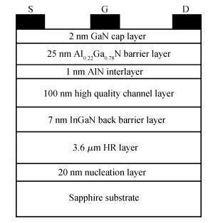
Fig. 1.
Cross-section of the fabricated AlGaN/GaN HEMT
SEMICONDUCTOR DEVICES
Xiaojia Wan1, 2, Xiaoliang Wang1, 2, 3, , Hongling Xiao1, 2, Chun Feng1, 2, Lijuan Jiang1, 2, Shenqi Qu1, 2, Zhanguo Wang1, 2 and Xun Hou3
Corresponding author: Wang Xiaoliang, xlwang@semi.ac.cn
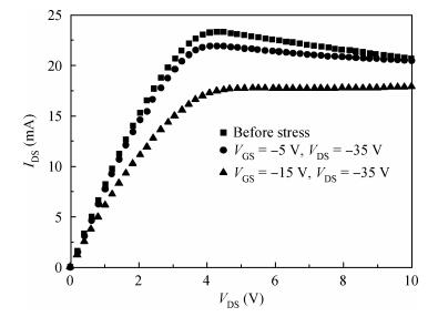
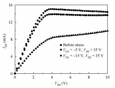
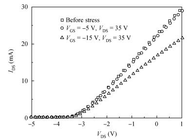
Abstract: Current collapses were studied, which were observed in AlGaN/GaN high electron mobility transistors (HEMTs) with and without InGaN back barrier (BB) as a result of short-term bias stress. More serious drain current collapses were observed in InGaN BB AlGaN/GaN HEMTs compared with the traditional HEMTs. The results indicate that the defects and surface states induced by the InGaN BB layer may enhance the current collapse. The surface states may be the primary mechanism of the origination of current collapse in AlGaN/GaN HEMTs for short-term direct current stress.
Keywords: AlGaN/GaN HEMT, InGaN, current collapse, surface states
| [1] |
Khan M A, Chen Q, Shur M S, et al. Microwave operation of GaN/AlGaN-doped channel heterostructure field effect transistors. IEEE Electron Device Lett, 1996, 17(7):325 doi: 10.1109/55.506356
|
| [2] |
Tang J, Wang X L, Xiao H L, et al. AlGaN/GaN/InGaN/GaN DH-HEMTs structure with an AlN interlayer grown by MOCVD. Phys Solidi Status C, 2008, 5(9):2982 doi: 10.1002/pssc.v5:9
|
| [3] |
Kikkawa T. Highly reliable 250 W GaN high electron mobility transistor power amplifier. Jpn J Appl Phys, 2005, 44(7):4896 http://global-sei.com/technology/tr/bn81/pdf/81-08.pdf
|
| [4] |
Meneghesso G, Verzellesi G, Danesin F, et al. Reliability of GaN high electron-mobility transistors:state of the art and perspectives. IEEE Trans Device Mater Rel, 2008, 8(2):332 doi: 10.1109/TDMR.2008.923743
|
| [5] |
Tapajna M, Simms R J T, Pei Y, et al. Integrated optical and electrical analysis:identifying location and properties of traps in AlGaN/GaN HEMTs during electrical stress. IEEE Electron Device Lett, 2010, 31(7):662 doi: 10.1109/LED.2010.2047092
|
| [6] |
Tapajna M, Kaun S W, Wong M H, et al. Influence of threading dislocation density on early degradation in AlGaN/GaN high electron mobility transistors. Appl Phys Lett, 2011, 99(22):223 http://sav-sk.academia.edu/Departments/Institute_of_Electrical_Engineering/Documents
|
| [7] |
Mizutani T, Ohno Y, Akita M, et al. A study on current collapse in AlGaN/GaN HEMTs induced by bias stress. IEEE Trans Electron Devices, 2003, 50(10):2015 doi: 10.1109/TED.2003.816549
|
| [8] |
Higashiwaki M, Mimura T, Matsui T. GaN-based FETs using Cat-CVD SiN passivation for millimeter-wave applications. Thin Solid Films, 2007, 516(2008):548 http://www.doc88.com/p-907289095544.html
|
| [9] |
Liu J, Zhou Y, Zhu J, et al. AlGaN/GaN/InGaN/GaN DH-HEMTs with an InGaN notch for enhanced carrier confinement. IEEE Electron Device Lett, 2006, 27(1):10 doi: 10.1109/LED.2005.861027
|
| [10] |
Klein P B, Binari S C, Freitas J A, et al. Photoionization spectroscopy of traps in GaN metal-semiconductor field-effect transistors. J Appl Phys, 2000, 88(5):2843 doi: 10.1063/1.1287127
|
| [11] |
Gu W P, Hao Y, Zhang J C, et al. Degradation under high-field stress and gate stress of AlGaN/GaN HEMTs. Chin Phys Soc, 2009, 58(1):511 http://www.sciencedirect.com/science/article/pii/S0026271417302494
|
| [12] |
Bi Y, Wang X L, Xiao H L, et al. The influence of the InGaN back-barrier on the properties of Al0.3Ga0.7N/AlN/GaN/InGaN/GaN structure. Eur Phys J Appl Phys, 2011, 55:10102 doi: 10.1051/epjap/2011110184
|
| [13] |
Vetury R, Zhang N Q, Keller S, et al. The impact of surface states on the DC and RF characteristics of AlGaN/GaN HFETs. IEEE Trans Electron Devices, 2001, 48(3):560 doi: 10.1109/16.906451
|
| [14] |
Mittereder J A, Binari S C, Klein P B, et al. Current collapse induced in AlGaN/GaN high-electron-mobility transistors by bias stress. Appl Phys Lett, 2003, 83(8):1650 doi: 10.1063/1.1604472
|


Article views: 3044 Times PDF downloads: 33 Times Cited by: 0 Times
Received: 04 March 2013 Revised: Online: Published: 01 October 2013
| Citation: |
Xiaojia Wan, Xiaoliang Wang, Hongling Xiao, Chun Feng, Lijuan Jiang, Shenqi Qu, Zhanguo Wang, Xun Hou. Investigation of the current collapse induced in InGaN back barrier AlGaN/GaN high electron mobility transistors[J]. Journal of Semiconductors, 2013, 34(10): 104002. doi: 10.1088/1674-4926/34/10/104002
****
X J Wan, X L Wang, H L Xiao, C Feng, L J Jiang, S Q Qu, Z G Wang, X Hou. Investigation of the current collapse induced in InGaN back barrier AlGaN/GaN high electron mobility transistors[J]. J. Semicond., 2013, 34(10): 104002. doi: 10.1088/1674-4926/34/10/104002.

|
| [1] |
Khan M A, Chen Q, Shur M S, et al. Microwave operation of GaN/AlGaN-doped channel heterostructure field effect transistors. IEEE Electron Device Lett, 1996, 17(7):325 doi: 10.1109/55.506356
|
| [2] |
Tang J, Wang X L, Xiao H L, et al. AlGaN/GaN/InGaN/GaN DH-HEMTs structure with an AlN interlayer grown by MOCVD. Phys Solidi Status C, 2008, 5(9):2982 doi: 10.1002/pssc.v5:9
|
| [3] |
Kikkawa T. Highly reliable 250 W GaN high electron mobility transistor power amplifier. Jpn J Appl Phys, 2005, 44(7):4896 http://global-sei.com/technology/tr/bn81/pdf/81-08.pdf
|
| [4] |
Meneghesso G, Verzellesi G, Danesin F, et al. Reliability of GaN high electron-mobility transistors:state of the art and perspectives. IEEE Trans Device Mater Rel, 2008, 8(2):332 doi: 10.1109/TDMR.2008.923743
|
| [5] |
Tapajna M, Simms R J T, Pei Y, et al. Integrated optical and electrical analysis:identifying location and properties of traps in AlGaN/GaN HEMTs during electrical stress. IEEE Electron Device Lett, 2010, 31(7):662 doi: 10.1109/LED.2010.2047092
|
| [6] |
Tapajna M, Kaun S W, Wong M H, et al. Influence of threading dislocation density on early degradation in AlGaN/GaN high electron mobility transistors. Appl Phys Lett, 2011, 99(22):223 http://sav-sk.academia.edu/Departments/Institute_of_Electrical_Engineering/Documents
|
| [7] |
Mizutani T, Ohno Y, Akita M, et al. A study on current collapse in AlGaN/GaN HEMTs induced by bias stress. IEEE Trans Electron Devices, 2003, 50(10):2015 doi: 10.1109/TED.2003.816549
|
| [8] |
Higashiwaki M, Mimura T, Matsui T. GaN-based FETs using Cat-CVD SiN passivation for millimeter-wave applications. Thin Solid Films, 2007, 516(2008):548 http://www.doc88.com/p-907289095544.html
|
| [9] |
Liu J, Zhou Y, Zhu J, et al. AlGaN/GaN/InGaN/GaN DH-HEMTs with an InGaN notch for enhanced carrier confinement. IEEE Electron Device Lett, 2006, 27(1):10 doi: 10.1109/LED.2005.861027
|
| [10] |
Klein P B, Binari S C, Freitas J A, et al. Photoionization spectroscopy of traps in GaN metal-semiconductor field-effect transistors. J Appl Phys, 2000, 88(5):2843 doi: 10.1063/1.1287127
|
| [11] |
Gu W P, Hao Y, Zhang J C, et al. Degradation under high-field stress and gate stress of AlGaN/GaN HEMTs. Chin Phys Soc, 2009, 58(1):511 http://www.sciencedirect.com/science/article/pii/S0026271417302494
|
| [12] |
Bi Y, Wang X L, Xiao H L, et al. The influence of the InGaN back-barrier on the properties of Al0.3Ga0.7N/AlN/GaN/InGaN/GaN structure. Eur Phys J Appl Phys, 2011, 55:10102 doi: 10.1051/epjap/2011110184
|
| [13] |
Vetury R, Zhang N Q, Keller S, et al. The impact of surface states on the DC and RF characteristics of AlGaN/GaN HFETs. IEEE Trans Electron Devices, 2001, 48(3):560 doi: 10.1109/16.906451
|
| [14] |
Mittereder J A, Binari S C, Klein P B, et al. Current collapse induced in AlGaN/GaN high-electron-mobility transistors by bias stress. Appl Phys Lett, 2003, 83(8):1650 doi: 10.1063/1.1604472
|

 WeChat ID
Journal of Semiconductors © 2017 All Rights Reserved 京ICP备05085259号-2

 DownLoad:

