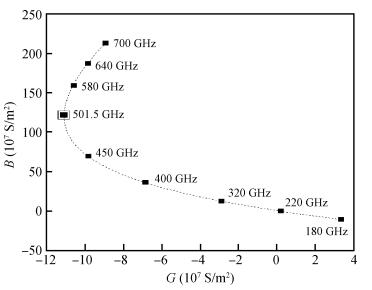
Fig. 1.
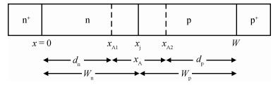
One-dimensional model of DDR IMPATT device
SEMICONDUCTOR DEVICES
Aritra Acharyya1, Jit Chakraborty2, Kausik Das2, Subir Datta2, Pritam De2, Suranjana Banerjee3 and J.P. Banerjee1
Abstract: The authors have carried out the large-signal characterization of silicon-based double-drift region (DDR) impact avalanche transit time (IMPATT) devices designed to operate up to 0.5 THz using a large-signal simulation method developed by the authors based on non-sinusoidal voltage excitation. The effect of band-to-band tunneling as well as parasitic series resistance on the large-signal properties of DDR Si IMPATTs have also been studied at different mm-wave and THz frequencies. Large-signal simulation results show that DDR Si IMPATT is capable of delivering peak RF power of 633.69 mW with 7.95% conversion efficiency at 94 GHz for 50% voltage modulation, whereas peak RF power output and efficiency fall to 81.08 mW and 2.01% respectively at 0.5 THz for same voltage modulation. The simulation results are compared with the experimental results and are found to be in close agreement.
Keywords: band to band tunneling, DDR silicon IMPATTs, large-signal simulation, millimeter-wave, series resistance, terahertz regime
| [1] |
Midford T A, Bernick R L. Millimeter wave CW IMPATT diodes and oscillators. IEEE Trans Microw Theory Tech, 1979, 27:483 doi: 10.1109/TMTT.1979.1129653
|
| [2] |
Chang Y, Hellum J M, Paul J A, et al. Millimeter-wave IMPATT sources for communication applications. IEEE MTT-S International Microwave Symposium Digest, 1977:216 http://ieeexplore.ieee.org/document/1124410/
|
| [3] |
Gray W W, Kikushima L, Morentc N P, et al. Applying IMPATT power sources to modern microwave systems. IEEE J Solid-State Circuits, 1969, 4:409 doi: 10.1109/JSSC.1969.1050046
|
| [4] |
Miswa T. Negative resistance in p-n junctions under avalanche breakdown conditions. IEEE Trans Electron Devices, 1966, 33:137 http://adsabs.harvard.edu/abs/1966ITED...13..143.
|
| [5] |
Gilden M, Hines M E. Electronic tuning effects in the read microwave avalanche diode. IEEE Trans Electron Devices, 1966, 13(1):169 http://adsabs.harvard.edu/abs/1966ITED...13E.169G
|
| [6] |
Gummel H K, Scharfetter D L. Avalanche region of IMPATT diodes. Bell Syst Tech J, 1966, 45:1797 doi: 10.1002/bltj.1966.45.issue-10
|
| [7] |
Roy S K, Sridharan M, Ghosh R, et al. Computer method for the dc field and carrier current profiles in the IMPATT device starting from the field extremum in the depletion layer. In:Miller J H, ed. Proceedings of the 1st Conference on Numerical Analysis of Semiconductor Devices (NASECODE Ⅰ), Dublin, Ireland, 1979:266 http://www.oalib.com/paper/3065525
|
| [8] |
Roy S K, Banerjee J P, Pati S P. A computer analysis of the distribution of high frequency negative resistance in the depletion layer of IMPATT diodes. Proceedings of 4th Conf on Num Anal of Semiconductor Devices (NASECODE Ⅳ), Dublin:Boole, 1985:494 doi: 10.1007%2FBF00619715.pdf
|
| [9] |
Acharyya A, Banerjee S, Banerjee J P. Dependence of DC and small-signal properties of double drift region silicon IMPATT device on junction temperature. J Electron Devices, 2012, 12:725 doi: 10.1007%2F978-81-322-2012-1_51.pdf
|
| [10] |
Acharyya A, Mukherjee M, Banerjee J P. Influence of tunnel current on DC and dynamic properties of silicon based terahertz IMPATT source. Terahertz Science and Technology, 2011, 4:26 doi: 10.1080/00207217.2014.982211?scroll=top&needAccess=true
|
| [11] |
Acharyya A, Banerjee S, Banerjee J P. Effect of package parasitics on the millimeter-wave performance of DDR silicon IMPATT device operating at W-band. J Electron Devices, 2012, 13:960 http://citeseerx.ist.psu.edu/viewdoc/download?doi=10.1.1.667.5333&rep=rep1&type=pdf
|
| [12] |
Acharyya A, Banerjee J P. Design and optimization of pulsed mode silicon based DDR IMPATT diode operating at 0.3 THz. International Journal of Engineering Science and Technology, 2011, 3:332 http://www.oalib.com/paper/2111670
|
| [13] |
Gummel H K, Blue J L. A small-signal theory of avalanche noise in IMPATT diodes. IEEE Trans Electron Devices, 1967, 14(9):569 doi: 10.1109/T-ED.1967.16005
|
| [14] |
Evans W J, Haddad G I. A large-signal analysis of IMPATT diodes. IEEE Trans Electron Devices, 1968, 15(10):708 doi: 10.1109/T-ED.1968.16503
|
| [15] |
Scharfetter D L, Gummel H K. Large-signal analysis of a silicon read diode oscillator. IEEE Trans Electron Devices, 1969, 6(1):64 doi: 10.1007/s10825-006-0016-7
|
| [16] |
Gupta M S, Lomax R J. A current-excited large-signal analysis of IMPATT devices and its circuit implementations. IEEE Trans Electron Devices, 1973, 20:395 doi: 10.1109/T-ED.1973.17661
|
| [17] |
Acharyya A, Banerjee J P. Prospects of IMPATT devices based on wide bandgap semiconductors as potential terahertz sources. Applied Nanoscience, 2012, DOI: DOI:10.1007/s13204-012-0172-y
|
| [18] |
Acharyya A, Banerjee J P. Potentiality of IMPATT devices as terahertz source:an avalanche response time based approach to determine the upper cut-off frequency limits. IETE Journal of Research, 2013, 59, in press doi: 10.4103/0377-2063.113029
|
| [19] |
Acharyya A, Banerjee S, Banerjee J P. Calculation of avalanche response time for determining the high frequency performance limitations of IMPATT devices. J Electron Devices, 2012, 12:756
|
| [20] |
Acharyya A, Banerjee J P. Analysis of photo-irradiated double-drift region silicon impact avalanche transit time devices in the millimeter-wave and terahertz regime. Terahertz Science and Technology, 2012, 5:97 doi: 10.1080/00207217.2013.830460?src=recsys
|
| [21] |
Acharyya A, Banerjee S, Banerjee J P. Effect of junction temperature on the large-signal properties of a 94 GHz silicon based double-drift region impact avalanche transit time device. Journal of Semiconductors, 2013, 34:024001 doi: 10.1088/1674-4926/34/2/024001
|
| [22] |
Acharyya A, Banerjee S, Banerjee J P. Large-signal simulation of 94 GHz pulsed DDR silicon IMPATTs including the temperature transient effect. Radioengineering, 2012, 21:1218 doi: 10.1007/s10825-013-0470-y
|
| [23] |
Acharyya A, Banerjee S, Banerjee J P. A proposed simulation technique to study the series resistance and related millimeter-wave properties of Ka-band Si IMPATTs from the electric field snapshots. International Journal of Microwave and Wireless Technologies, available on CJO2013. DOI: DOI:10.1017/S1759078712000839
|
| [24] |
Elta M E. The effect of mixed tunneling and avalanche breakdown on microwave transit-time diodes. PhD Dissertation, Electron Physics Laboratory, Univ. of Mich. , Ann Arbor, MI, Tech. Rep, 1978
|
| [25] |
Kane E O. Theory of tunneling. J Appl Phys, 1961, 32:83 doi: 10.1063/1.1735965
|
| [26] |
Acharyya A, Mukherjee M, Banerjee J P. Influence of tunnel current on DC and dynamic properties of silicon based terahertz IMPATT source. Terahertz Science and Technology, 2011, 4(1):26 doi: 10.1080/00207217.2014.982211?scroll=top&needAccess=true
|
| [27] |
Dash G N, Pati S P. A generalized simulation method for IMPATT mode operation and studies on the influence of tunnel current on IMPATT properties. Semicond Sci Technol, 1992, 7:222 doi: 10.1088/0268-1242/7/2/008
|
| [28] |
Sze S M, Ryder R M. Microwave avalanche diodes. Proc IEEE, Special Issue on Microwave Semiconductor Devices, 1971, 59(8):1140 https://www.elsevier.com/books/practical-microwave-electron-devices/unknown/978-0-12-374700-6
|
| [29] |
Acharyya A, Mukherjee J, Mukherjee M, et al. Heat sink design for IMPATT diode sources with different base materials operating at 94 GHz. Archives of Physics Research, 2011, 2(1):107 http://airccj.org/CSCP/vol3/csit3237.pdf
|
| [30] |
Acharyya A, Pal B, Banerjee J P. Temperature distribution inside semi-infinite heat sinks for IMPATT sources. International Journal of Engineering Science and Technology, 2010, 2(10):5142 http://www.oalib.com/paper/1312864
|
| [31] |
Grant W N. Electron and hole ionization rates in epitaxial silicon. Solid-State Electron, 1973, 16(10):1189 doi: 10.1016/0038-1101(73)90147-0
|
| [32] |
Canali C, Ottaviani G, Quaranta A A. Drift velocity of electrons and holes and associated anisotropic effects in silicon. J Phys Chem Solids, 1971, 32(8):1707 doi: 10.1016/S0022-3697(71)80137-3
|
| [33] |
Zeghbroeck B V. Principles of semiconductor devices. Colorado Press, 2011
|
| [34] |
Electronic Archive: New Semiconductor Materials, Characteristics and Properties. http://www.ioffe.ru/SVA/NSM/Semicond/Si/index.html
|
| [35] |
Kurokawa K. Some basic characteristics to broadband negative resistance oscillators. Bell Syst Tech J, 1969, 48:1937 doi: 10.1002/bltj.1969.48.issue-6
|
| [36] |
Luy J F, Casel A, Behr W, et al. A 90-GHz double-drift IMPATT diode made with Si MBE. IEEE Trans Electron Devices, 1987, 34:1084 doi: 10.1109/T-ED.1987.23049
|
| [37] |
Wollitzer M, Buchler J, Schafflr F, et al. D-band Si-IMPATT diodes with 300 mW CW output power at 140 GHz. Electron Lett, 1996, 32:122 doi: 10.1049/el:19960088
|
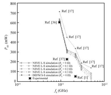
Table 1. Structural, doping and other parameters of base material Si
 |
Table 2. Static parameters of base material Si
 |
Table 3. Large-signal parameters of base material Si
 |
Table 4.
Peak tunneling generation rates (
 |
Table 5. The sensitivity analysis and the effect of tunneling on the large-signal properties of DDR diamond and Si IMPATTs at different mm-wave and THz frequencies by taking 50% voltage modulation
 |
Table 6.
RF power outputs and DC to RF conversion efficiencies for different values of
 |
| [1] |
Midford T A, Bernick R L. Millimeter wave CW IMPATT diodes and oscillators. IEEE Trans Microw Theory Tech, 1979, 27:483 doi: 10.1109/TMTT.1979.1129653
|
| [2] |
Chang Y, Hellum J M, Paul J A, et al. Millimeter-wave IMPATT sources for communication applications. IEEE MTT-S International Microwave Symposium Digest, 1977:216 http://ieeexplore.ieee.org/document/1124410/
|
| [3] |
Gray W W, Kikushima L, Morentc N P, et al. Applying IMPATT power sources to modern microwave systems. IEEE J Solid-State Circuits, 1969, 4:409 doi: 10.1109/JSSC.1969.1050046
|
| [4] |
Miswa T. Negative resistance in p-n junctions under avalanche breakdown conditions. IEEE Trans Electron Devices, 1966, 33:137 http://adsabs.harvard.edu/abs/1966ITED...13..143.
|
| [5] |
Gilden M, Hines M E. Electronic tuning effects in the read microwave avalanche diode. IEEE Trans Electron Devices, 1966, 13(1):169 http://adsabs.harvard.edu/abs/1966ITED...13E.169G
|
| [6] |
Gummel H K, Scharfetter D L. Avalanche region of IMPATT diodes. Bell Syst Tech J, 1966, 45:1797 doi: 10.1002/bltj.1966.45.issue-10
|
| [7] |
Roy S K, Sridharan M, Ghosh R, et al. Computer method for the dc field and carrier current profiles in the IMPATT device starting from the field extremum in the depletion layer. In:Miller J H, ed. Proceedings of the 1st Conference on Numerical Analysis of Semiconductor Devices (NASECODE Ⅰ), Dublin, Ireland, 1979:266 http://www.oalib.com/paper/3065525
|
| [8] |
Roy S K, Banerjee J P, Pati S P. A computer analysis of the distribution of high frequency negative resistance in the depletion layer of IMPATT diodes. Proceedings of 4th Conf on Num Anal of Semiconductor Devices (NASECODE Ⅳ), Dublin:Boole, 1985:494 doi: 10.1007%2FBF00619715.pdf
|
| [9] |
Acharyya A, Banerjee S, Banerjee J P. Dependence of DC and small-signal properties of double drift region silicon IMPATT device on junction temperature. J Electron Devices, 2012, 12:725 doi: 10.1007%2F978-81-322-2012-1_51.pdf
|
| [10] |
Acharyya A, Mukherjee M, Banerjee J P. Influence of tunnel current on DC and dynamic properties of silicon based terahertz IMPATT source. Terahertz Science and Technology, 2011, 4:26 doi: 10.1080/00207217.2014.982211?scroll=top&needAccess=true
|
| [11] |
Acharyya A, Banerjee S, Banerjee J P. Effect of package parasitics on the millimeter-wave performance of DDR silicon IMPATT device operating at W-band. J Electron Devices, 2012, 13:960 http://citeseerx.ist.psu.edu/viewdoc/download?doi=10.1.1.667.5333&rep=rep1&type=pdf
|
| [12] |
Acharyya A, Banerjee J P. Design and optimization of pulsed mode silicon based DDR IMPATT diode operating at 0.3 THz. International Journal of Engineering Science and Technology, 2011, 3:332 http://www.oalib.com/paper/2111670
|
| [13] |
Gummel H K, Blue J L. A small-signal theory of avalanche noise in IMPATT diodes. IEEE Trans Electron Devices, 1967, 14(9):569 doi: 10.1109/T-ED.1967.16005
|
| [14] |
Evans W J, Haddad G I. A large-signal analysis of IMPATT diodes. IEEE Trans Electron Devices, 1968, 15(10):708 doi: 10.1109/T-ED.1968.16503
|
| [15] |
Scharfetter D L, Gummel H K. Large-signal analysis of a silicon read diode oscillator. IEEE Trans Electron Devices, 1969, 6(1):64 doi: 10.1007/s10825-006-0016-7
|
| [16] |
Gupta M S, Lomax R J. A current-excited large-signal analysis of IMPATT devices and its circuit implementations. IEEE Trans Electron Devices, 1973, 20:395 doi: 10.1109/T-ED.1973.17661
|
| [17] |
Acharyya A, Banerjee J P. Prospects of IMPATT devices based on wide bandgap semiconductors as potential terahertz sources. Applied Nanoscience, 2012, DOI: DOI:10.1007/s13204-012-0172-y
|
| [18] |
Acharyya A, Banerjee J P. Potentiality of IMPATT devices as terahertz source:an avalanche response time based approach to determine the upper cut-off frequency limits. IETE Journal of Research, 2013, 59, in press doi: 10.4103/0377-2063.113029
|
| [19] |
Acharyya A, Banerjee S, Banerjee J P. Calculation of avalanche response time for determining the high frequency performance limitations of IMPATT devices. J Electron Devices, 2012, 12:756
|
| [20] |
Acharyya A, Banerjee J P. Analysis of photo-irradiated double-drift region silicon impact avalanche transit time devices in the millimeter-wave and terahertz regime. Terahertz Science and Technology, 2012, 5:97 doi: 10.1080/00207217.2013.830460?src=recsys
|
| [21] |
Acharyya A, Banerjee S, Banerjee J P. Effect of junction temperature on the large-signal properties of a 94 GHz silicon based double-drift region impact avalanche transit time device. Journal of Semiconductors, 2013, 34:024001 doi: 10.1088/1674-4926/34/2/024001
|
| [22] |
Acharyya A, Banerjee S, Banerjee J P. Large-signal simulation of 94 GHz pulsed DDR silicon IMPATTs including the temperature transient effect. Radioengineering, 2012, 21:1218 doi: 10.1007/s10825-013-0470-y
|
| [23] |
Acharyya A, Banerjee S, Banerjee J P. A proposed simulation technique to study the series resistance and related millimeter-wave properties of Ka-band Si IMPATTs from the electric field snapshots. International Journal of Microwave and Wireless Technologies, available on CJO2013. DOI: DOI:10.1017/S1759078712000839
|
| [24] |
Elta M E. The effect of mixed tunneling and avalanche breakdown on microwave transit-time diodes. PhD Dissertation, Electron Physics Laboratory, Univ. of Mich. , Ann Arbor, MI, Tech. Rep, 1978
|
| [25] |
Kane E O. Theory of tunneling. J Appl Phys, 1961, 32:83 doi: 10.1063/1.1735965
|
| [26] |
Acharyya A, Mukherjee M, Banerjee J P. Influence of tunnel current on DC and dynamic properties of silicon based terahertz IMPATT source. Terahertz Science and Technology, 2011, 4(1):26 doi: 10.1080/00207217.2014.982211?scroll=top&needAccess=true
|
| [27] |
Dash G N, Pati S P. A generalized simulation method for IMPATT mode operation and studies on the influence of tunnel current on IMPATT properties. Semicond Sci Technol, 1992, 7:222 doi: 10.1088/0268-1242/7/2/008
|
| [28] |
Sze S M, Ryder R M. Microwave avalanche diodes. Proc IEEE, Special Issue on Microwave Semiconductor Devices, 1971, 59(8):1140 https://www.elsevier.com/books/practical-microwave-electron-devices/unknown/978-0-12-374700-6
|
| [29] |
Acharyya A, Mukherjee J, Mukherjee M, et al. Heat sink design for IMPATT diode sources with different base materials operating at 94 GHz. Archives of Physics Research, 2011, 2(1):107 http://airccj.org/CSCP/vol3/csit3237.pdf
|
| [30] |
Acharyya A, Pal B, Banerjee J P. Temperature distribution inside semi-infinite heat sinks for IMPATT sources. International Journal of Engineering Science and Technology, 2010, 2(10):5142 http://www.oalib.com/paper/1312864
|
| [31] |
Grant W N. Electron and hole ionization rates in epitaxial silicon. Solid-State Electron, 1973, 16(10):1189 doi: 10.1016/0038-1101(73)90147-0
|
| [32] |
Canali C, Ottaviani G, Quaranta A A. Drift velocity of electrons and holes and associated anisotropic effects in silicon. J Phys Chem Solids, 1971, 32(8):1707 doi: 10.1016/S0022-3697(71)80137-3
|
| [33] |
Zeghbroeck B V. Principles of semiconductor devices. Colorado Press, 2011
|
| [34] |
Electronic Archive: New Semiconductor Materials, Characteristics and Properties. http://www.ioffe.ru/SVA/NSM/Semicond/Si/index.html
|
| [35] |
Kurokawa K. Some basic characteristics to broadband negative resistance oscillators. Bell Syst Tech J, 1969, 48:1937 doi: 10.1002/bltj.1969.48.issue-6
|
| [36] |
Luy J F, Casel A, Behr W, et al. A 90-GHz double-drift IMPATT diode made with Si MBE. IEEE Trans Electron Devices, 1987, 34:1084 doi: 10.1109/T-ED.1987.23049
|
| [37] |
Wollitzer M, Buchler J, Schafflr F, et al. D-band Si-IMPATT diodes with 300 mW CW output power at 140 GHz. Electron Lett, 1996, 32:122 doi: 10.1049/el:19960088
|


Article views: 2749 Times PDF downloads: 10 Times Cited by: 0 Times
Received: 06 February 2013 Revised: 11 May 2013 Online: Published: 01 October 2013
| Citation: |
Aritra Acharyya, Jit Chakraborty, Kausik Das, Subir Datta, Pritam De, Suranjana Banerjee, J.P. Banerjee. Large-signal characterization of DDR silicon IMPATTs operating in millimeter-wave and terahertz regime[J]. Journal of Semiconductors, 2013, 34(10): 104003. doi: 10.1088/1674-4926/34/10/104003
****
A Acharyya, J Chakraborty, K Das, S Datta, P De, S Banerjee, J.P. Banerjee. Large-signal characterization of DDR silicon IMPATTs operating in millimeter-wave and terahertz regime[J]. J. Semicond., 2013, 34(10): 104003. doi: 10.1088/1674-4926/34/10/104003.

|
| [1] |
Midford T A, Bernick R L. Millimeter wave CW IMPATT diodes and oscillators. IEEE Trans Microw Theory Tech, 1979, 27:483 doi: 10.1109/TMTT.1979.1129653
|
| [2] |
Chang Y, Hellum J M, Paul J A, et al. Millimeter-wave IMPATT sources for communication applications. IEEE MTT-S International Microwave Symposium Digest, 1977:216 http://ieeexplore.ieee.org/document/1124410/
|
| [3] |
Gray W W, Kikushima L, Morentc N P, et al. Applying IMPATT power sources to modern microwave systems. IEEE J Solid-State Circuits, 1969, 4:409 doi: 10.1109/JSSC.1969.1050046
|
| [4] |
Miswa T. Negative resistance in p-n junctions under avalanche breakdown conditions. IEEE Trans Electron Devices, 1966, 33:137 http://adsabs.harvard.edu/abs/1966ITED...13..143.
|
| [5] |
Gilden M, Hines M E. Electronic tuning effects in the read microwave avalanche diode. IEEE Trans Electron Devices, 1966, 13(1):169 http://adsabs.harvard.edu/abs/1966ITED...13E.169G
|
| [6] |
Gummel H K, Scharfetter D L. Avalanche region of IMPATT diodes. Bell Syst Tech J, 1966, 45:1797 doi: 10.1002/bltj.1966.45.issue-10
|
| [7] |
Roy S K, Sridharan M, Ghosh R, et al. Computer method for the dc field and carrier current profiles in the IMPATT device starting from the field extremum in the depletion layer. In:Miller J H, ed. Proceedings of the 1st Conference on Numerical Analysis of Semiconductor Devices (NASECODE Ⅰ), Dublin, Ireland, 1979:266 http://www.oalib.com/paper/3065525
|
| [8] |
Roy S K, Banerjee J P, Pati S P. A computer analysis of the distribution of high frequency negative resistance in the depletion layer of IMPATT diodes. Proceedings of 4th Conf on Num Anal of Semiconductor Devices (NASECODE Ⅳ), Dublin:Boole, 1985:494 doi: 10.1007%2FBF00619715.pdf
|
| [9] |
Acharyya A, Banerjee S, Banerjee J P. Dependence of DC and small-signal properties of double drift region silicon IMPATT device on junction temperature. J Electron Devices, 2012, 12:725 doi: 10.1007%2F978-81-322-2012-1_51.pdf
|
| [10] |
Acharyya A, Mukherjee M, Banerjee J P. Influence of tunnel current on DC and dynamic properties of silicon based terahertz IMPATT source. Terahertz Science and Technology, 2011, 4:26 doi: 10.1080/00207217.2014.982211?scroll=top&needAccess=true
|
| [11] |
Acharyya A, Banerjee S, Banerjee J P. Effect of package parasitics on the millimeter-wave performance of DDR silicon IMPATT device operating at W-band. J Electron Devices, 2012, 13:960 http://citeseerx.ist.psu.edu/viewdoc/download?doi=10.1.1.667.5333&rep=rep1&type=pdf
|
| [12] |
Acharyya A, Banerjee J P. Design and optimization of pulsed mode silicon based DDR IMPATT diode operating at 0.3 THz. International Journal of Engineering Science and Technology, 2011, 3:332 http://www.oalib.com/paper/2111670
|
| [13] |
Gummel H K, Blue J L. A small-signal theory of avalanche noise in IMPATT diodes. IEEE Trans Electron Devices, 1967, 14(9):569 doi: 10.1109/T-ED.1967.16005
|
| [14] |
Evans W J, Haddad G I. A large-signal analysis of IMPATT diodes. IEEE Trans Electron Devices, 1968, 15(10):708 doi: 10.1109/T-ED.1968.16503
|
| [15] |
Scharfetter D L, Gummel H K. Large-signal analysis of a silicon read diode oscillator. IEEE Trans Electron Devices, 1969, 6(1):64 doi: 10.1007/s10825-006-0016-7
|
| [16] |
Gupta M S, Lomax R J. A current-excited large-signal analysis of IMPATT devices and its circuit implementations. IEEE Trans Electron Devices, 1973, 20:395 doi: 10.1109/T-ED.1973.17661
|
| [17] |
Acharyya A, Banerjee J P. Prospects of IMPATT devices based on wide bandgap semiconductors as potential terahertz sources. Applied Nanoscience, 2012, DOI: DOI:10.1007/s13204-012-0172-y
|
| [18] |
Acharyya A, Banerjee J P. Potentiality of IMPATT devices as terahertz source:an avalanche response time based approach to determine the upper cut-off frequency limits. IETE Journal of Research, 2013, 59, in press doi: 10.4103/0377-2063.113029
|
| [19] |
Acharyya A, Banerjee S, Banerjee J P. Calculation of avalanche response time for determining the high frequency performance limitations of IMPATT devices. J Electron Devices, 2012, 12:756
|
| [20] |
Acharyya A, Banerjee J P. Analysis of photo-irradiated double-drift region silicon impact avalanche transit time devices in the millimeter-wave and terahertz regime. Terahertz Science and Technology, 2012, 5:97 doi: 10.1080/00207217.2013.830460?src=recsys
|
| [21] |
Acharyya A, Banerjee S, Banerjee J P. Effect of junction temperature on the large-signal properties of a 94 GHz silicon based double-drift region impact avalanche transit time device. Journal of Semiconductors, 2013, 34:024001 doi: 10.1088/1674-4926/34/2/024001
|
| [22] |
Acharyya A, Banerjee S, Banerjee J P. Large-signal simulation of 94 GHz pulsed DDR silicon IMPATTs including the temperature transient effect. Radioengineering, 2012, 21:1218 doi: 10.1007/s10825-013-0470-y
|
| [23] |
Acharyya A, Banerjee S, Banerjee J P. A proposed simulation technique to study the series resistance and related millimeter-wave properties of Ka-band Si IMPATTs from the electric field snapshots. International Journal of Microwave and Wireless Technologies, available on CJO2013. DOI: DOI:10.1017/S1759078712000839
|
| [24] |
Elta M E. The effect of mixed tunneling and avalanche breakdown on microwave transit-time diodes. PhD Dissertation, Electron Physics Laboratory, Univ. of Mich. , Ann Arbor, MI, Tech. Rep, 1978
|
| [25] |
Kane E O. Theory of tunneling. J Appl Phys, 1961, 32:83 doi: 10.1063/1.1735965
|
| [26] |
Acharyya A, Mukherjee M, Banerjee J P. Influence of tunnel current on DC and dynamic properties of silicon based terahertz IMPATT source. Terahertz Science and Technology, 2011, 4(1):26 doi: 10.1080/00207217.2014.982211?scroll=top&needAccess=true
|
| [27] |
Dash G N, Pati S P. A generalized simulation method for IMPATT mode operation and studies on the influence of tunnel current on IMPATT properties. Semicond Sci Technol, 1992, 7:222 doi: 10.1088/0268-1242/7/2/008
|
| [28] |
Sze S M, Ryder R M. Microwave avalanche diodes. Proc IEEE, Special Issue on Microwave Semiconductor Devices, 1971, 59(8):1140 https://www.elsevier.com/books/practical-microwave-electron-devices/unknown/978-0-12-374700-6
|
| [29] |
Acharyya A, Mukherjee J, Mukherjee M, et al. Heat sink design for IMPATT diode sources with different base materials operating at 94 GHz. Archives of Physics Research, 2011, 2(1):107 http://airccj.org/CSCP/vol3/csit3237.pdf
|
| [30] |
Acharyya A, Pal B, Banerjee J P. Temperature distribution inside semi-infinite heat sinks for IMPATT sources. International Journal of Engineering Science and Technology, 2010, 2(10):5142 http://www.oalib.com/paper/1312864
|
| [31] |
Grant W N. Electron and hole ionization rates in epitaxial silicon. Solid-State Electron, 1973, 16(10):1189 doi: 10.1016/0038-1101(73)90147-0
|
| [32] |
Canali C, Ottaviani G, Quaranta A A. Drift velocity of electrons and holes and associated anisotropic effects in silicon. J Phys Chem Solids, 1971, 32(8):1707 doi: 10.1016/S0022-3697(71)80137-3
|
| [33] |
Zeghbroeck B V. Principles of semiconductor devices. Colorado Press, 2011
|
| [34] |
Electronic Archive: New Semiconductor Materials, Characteristics and Properties. http://www.ioffe.ru/SVA/NSM/Semicond/Si/index.html
|
| [35] |
Kurokawa K. Some basic characteristics to broadband negative resistance oscillators. Bell Syst Tech J, 1969, 48:1937 doi: 10.1002/bltj.1969.48.issue-6
|
| [36] |
Luy J F, Casel A, Behr W, et al. A 90-GHz double-drift IMPATT diode made with Si MBE. IEEE Trans Electron Devices, 1987, 34:1084 doi: 10.1109/T-ED.1987.23049
|
| [37] |
Wollitzer M, Buchler J, Schafflr F, et al. D-band Si-IMPATT diodes with 300 mW CW output power at 140 GHz. Electron Lett, 1996, 32:122 doi: 10.1049/el:19960088
|

 WeChat ID
Journal of Semiconductors © 2017 All Rights Reserved 京ICP备05085259号-2

 DownLoad: