Fig. 1.
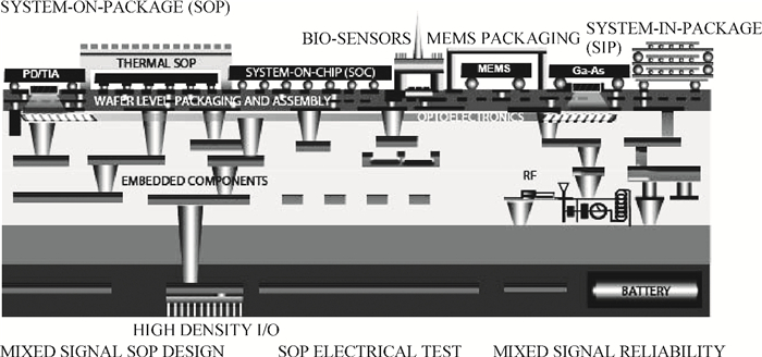
Schematic diagram of a system on package (SoP)[1].
SEMICONDUCTOR DEVICES
Tianxi Wang1, 2, Mei Han1, 2, Gaowei Xu1, and Le Luo1
Corresponding author: Xu Gaowei, xugw@mail.sim.ac.cn
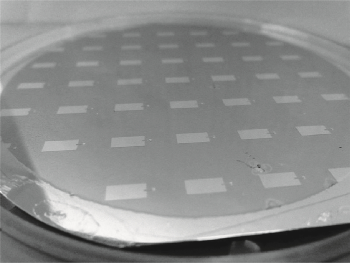
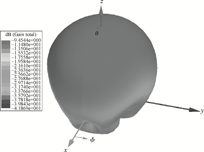
Abstract: This paper demonstrates a technique for microstrip patch antenna fabrication using a benzocyclobutene (BCB) dielectric. The most distinctive feature of this method is that the antenna is integrated on a low-resistance silicon wafer, and is fully compatible with the microwave multi-chip module packaging process. Low-permittivity dielectric BCB with excellent thermal and mechanical stability is employed to enhance the performance of the antenna. The as-fabricated antenna is characterized, and the experimental results show that the antenna resonates at 14.9 GHz with a 1.67% impedance bandwidth.
| [1] |
Rao R T, Madhavan S. Introduction to system-on-package (SoP):miniaturization of the entire system. USA:McGraw-Hill Prof Med/Tech, 2008, 3:81
|
| [2] |
Carchon G J, Raedt W D, Beyne E. Wafer-level packaging technology for high-Q on-chip inductors and transmission lines. IEEE Trans Microw Theory Tech, 2004, 52:1244 doi: 10.1109/TMTT.2004.825656
|
| [3] |
Ding X Y, Geng F, Luo L. Process development in metal/BCB multilayer interconnections of MMCM with embedded chip in Si substrate Microelectron Eng, 2009, 86: 335
|
| [4] |
Geng F, Ding X Y, Xu G W, et al. A wafer-scale packaging structure with monolithic microwave integrated circuits and passives embedded in a silicon substrate for multichip modules for radio frequency applications. J Micromech Microeng, 2009, 19:105011 doi: 10.1088/0960-1317/19/10/105011
|
| [5] |
Carrillo-Ramirez R, Jackson R W. A technique for interconnecting millimeter wave integrated circuits using BCB and bump bonds. IEEE Microw Wirel Compon Lett, 2003, 13:196 doi: 10.1109/LMWC.2003.811677
|
| [6] |
Ju C W, Park S S, Kim S J, et al. Effects of O2C2F6 plasma descum with RF cleaning on via formation in MCM-D substrate using photosensitive BCB. Electronic Components and Technology Conf. Orlando, FL, USA, 2001:1216
|
| [7] |
Tang J J, Ding X Y, Geng F, et al. Wafer-level multilayer integration of RF passives with thick BCB/metal interlayer connection in silicon-based SiP. Microsyst Technol, 2012, 18:119 doi: 10.1007/s00542-011-1370-3
|
| [8] |
Tilmans H A C, De Raedt W, Beyne E. MEMS for wireless communications:'from RF-MEMS components to RF-MEMS-SiP'. J Micromech Microeng, 2003, 13:S139 http://cat.inist.fr/?aModele=afficheN&cpsidt=14901609
|
| [9] |
Tang J J, Sun X W, Luo L. A wafer level multi-chip module process with thick photosensitive benzocyclobutene as dielectric for microwave application. J Micromech Microeng, 2011, 21:065035 doi: 10.1088/0960-1317/21/6/065035
|
| [10] |
Wadell B C. Transmission-line design handbook. Boston:Artech House, 1991 http://ci.nii.ac.jp/ncid/BA51343143
|
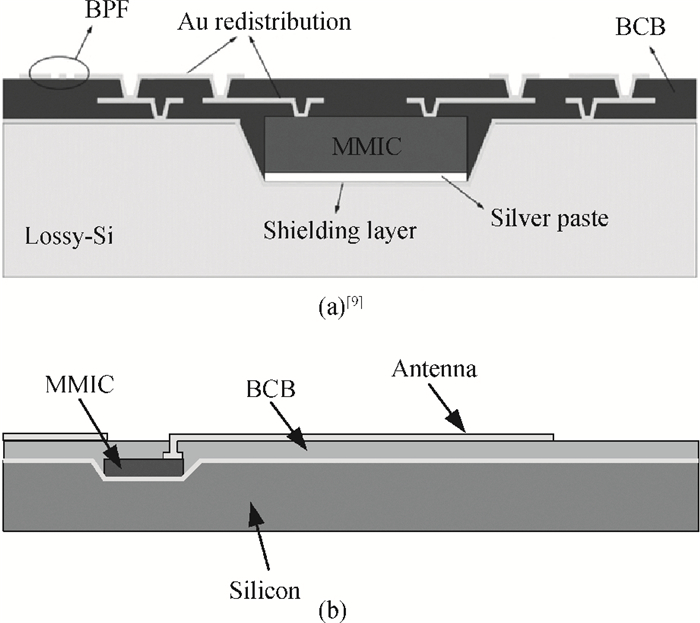
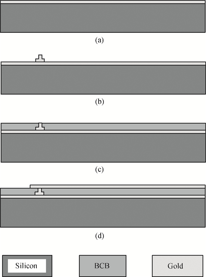
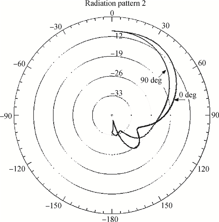
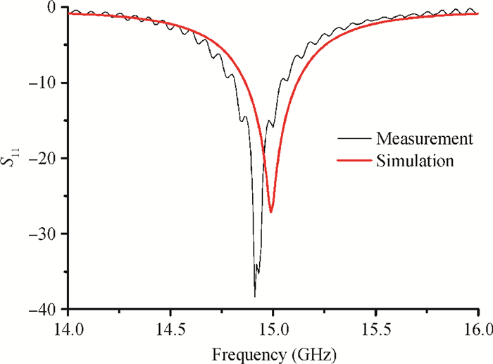
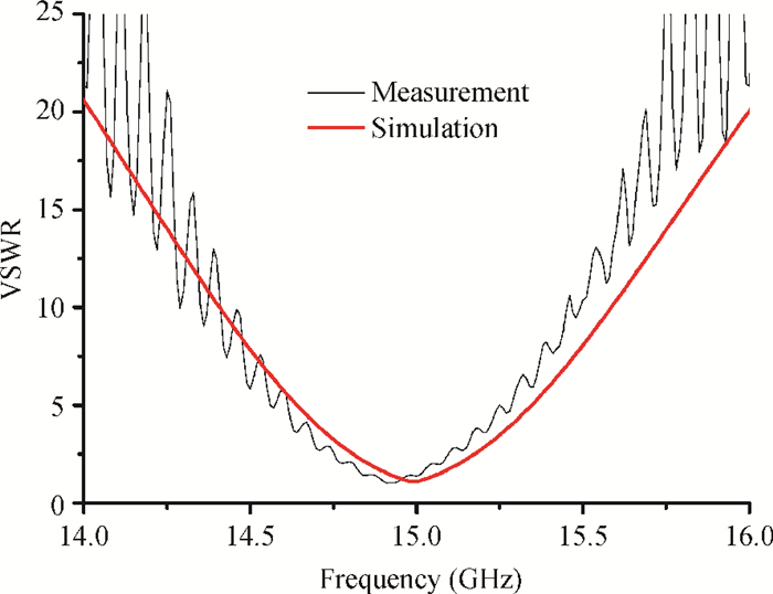
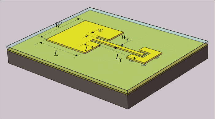
Table 1. The parameters of the microstrip patch antenna.

|
| [1] |
Rao R T, Madhavan S. Introduction to system-on-package (SoP):miniaturization of the entire system. USA:McGraw-Hill Prof Med/Tech, 2008, 3:81
|
| [2] |
Carchon G J, Raedt W D, Beyne E. Wafer-level packaging technology for high-Q on-chip inductors and transmission lines. IEEE Trans Microw Theory Tech, 2004, 52:1244 doi: 10.1109/TMTT.2004.825656
|
| [3] |
Ding X Y, Geng F, Luo L. Process development in metal/BCB multilayer interconnections of MMCM with embedded chip in Si substrate Microelectron Eng, 2009, 86: 335
|
| [4] |
Geng F, Ding X Y, Xu G W, et al. A wafer-scale packaging structure with monolithic microwave integrated circuits and passives embedded in a silicon substrate for multichip modules for radio frequency applications. J Micromech Microeng, 2009, 19:105011 doi: 10.1088/0960-1317/19/10/105011
|
| [5] |
Carrillo-Ramirez R, Jackson R W. A technique for interconnecting millimeter wave integrated circuits using BCB and bump bonds. IEEE Microw Wirel Compon Lett, 2003, 13:196 doi: 10.1109/LMWC.2003.811677
|
| [6] |
Ju C W, Park S S, Kim S J, et al. Effects of O2C2F6 plasma descum with RF cleaning on via formation in MCM-D substrate using photosensitive BCB. Electronic Components and Technology Conf. Orlando, FL, USA, 2001:1216
|
| [7] |
Tang J J, Ding X Y, Geng F, et al. Wafer-level multilayer integration of RF passives with thick BCB/metal interlayer connection in silicon-based SiP. Microsyst Technol, 2012, 18:119 doi: 10.1007/s00542-011-1370-3
|
| [8] |
Tilmans H A C, De Raedt W, Beyne E. MEMS for wireless communications:'from RF-MEMS components to RF-MEMS-SiP'. J Micromech Microeng, 2003, 13:S139 http://cat.inist.fr/?aModele=afficheN&cpsidt=14901609
|
| [9] |
Tang J J, Sun X W, Luo L. A wafer level multi-chip module process with thick photosensitive benzocyclobutene as dielectric for microwave application. J Micromech Microeng, 2011, 21:065035 doi: 10.1088/0960-1317/21/6/065035
|
| [10] |
Wadell B C. Transmission-line design handbook. Boston:Artech House, 1991 http://ci.nii.ac.jp/ncid/BA51343143
|


Article views: 4340 Times PDF downloads: 27 Times Cited by: 0 Times
Received: 21 March 2013 Revised: 13 April 2013 Online: Published: 01 October 2013
| Citation: |
Tianxi Wang, Mei Han, Gaowei Xu, Le Luo. Fabrication of a microstrip patch antenna integrated in low-resistance silicon wafer using a BCB dielectric[J]. Journal of Semiconductors, 2013, 34(10): 104008. doi: 10.1088/1674-4926/34/10/104008
****
T X Wang, M Han, G W Xu, L Luo. Fabrication of a microstrip patch antenna integrated in low-resistance silicon wafer using a BCB dielectric[J]. J. Semicond., 2013, 34(10): 104008. doi: 10.1088/1674-4926/34/10/104008.

|
| [1] |
Rao R T, Madhavan S. Introduction to system-on-package (SoP):miniaturization of the entire system. USA:McGraw-Hill Prof Med/Tech, 2008, 3:81
|
| [2] |
Carchon G J, Raedt W D, Beyne E. Wafer-level packaging technology for high-Q on-chip inductors and transmission lines. IEEE Trans Microw Theory Tech, 2004, 52:1244 doi: 10.1109/TMTT.2004.825656
|
| [3] |
Ding X Y, Geng F, Luo L. Process development in metal/BCB multilayer interconnections of MMCM with embedded chip in Si substrate Microelectron Eng, 2009, 86: 335
|
| [4] |
Geng F, Ding X Y, Xu G W, et al. A wafer-scale packaging structure with monolithic microwave integrated circuits and passives embedded in a silicon substrate for multichip modules for radio frequency applications. J Micromech Microeng, 2009, 19:105011 doi: 10.1088/0960-1317/19/10/105011
|
| [5] |
Carrillo-Ramirez R, Jackson R W. A technique for interconnecting millimeter wave integrated circuits using BCB and bump bonds. IEEE Microw Wirel Compon Lett, 2003, 13:196 doi: 10.1109/LMWC.2003.811677
|
| [6] |
Ju C W, Park S S, Kim S J, et al. Effects of O2C2F6 plasma descum with RF cleaning on via formation in MCM-D substrate using photosensitive BCB. Electronic Components and Technology Conf. Orlando, FL, USA, 2001:1216
|
| [7] |
Tang J J, Ding X Y, Geng F, et al. Wafer-level multilayer integration of RF passives with thick BCB/metal interlayer connection in silicon-based SiP. Microsyst Technol, 2012, 18:119 doi: 10.1007/s00542-011-1370-3
|
| [8] |
Tilmans H A C, De Raedt W, Beyne E. MEMS for wireless communications:'from RF-MEMS components to RF-MEMS-SiP'. J Micromech Microeng, 2003, 13:S139 http://cat.inist.fr/?aModele=afficheN&cpsidt=14901609
|
| [9] |
Tang J J, Sun X W, Luo L. A wafer level multi-chip module process with thick photosensitive benzocyclobutene as dielectric for microwave application. J Micromech Microeng, 2011, 21:065035 doi: 10.1088/0960-1317/21/6/065035
|
| [10] |
Wadell B C. Transmission-line design handbook. Boston:Artech House, 1991 http://ci.nii.ac.jp/ncid/BA51343143
|

 WeChat ID
Journal of Semiconductors © 2017 All Rights Reserved 京ICP备05085259号-2

 DownLoad: