Fig. 1.
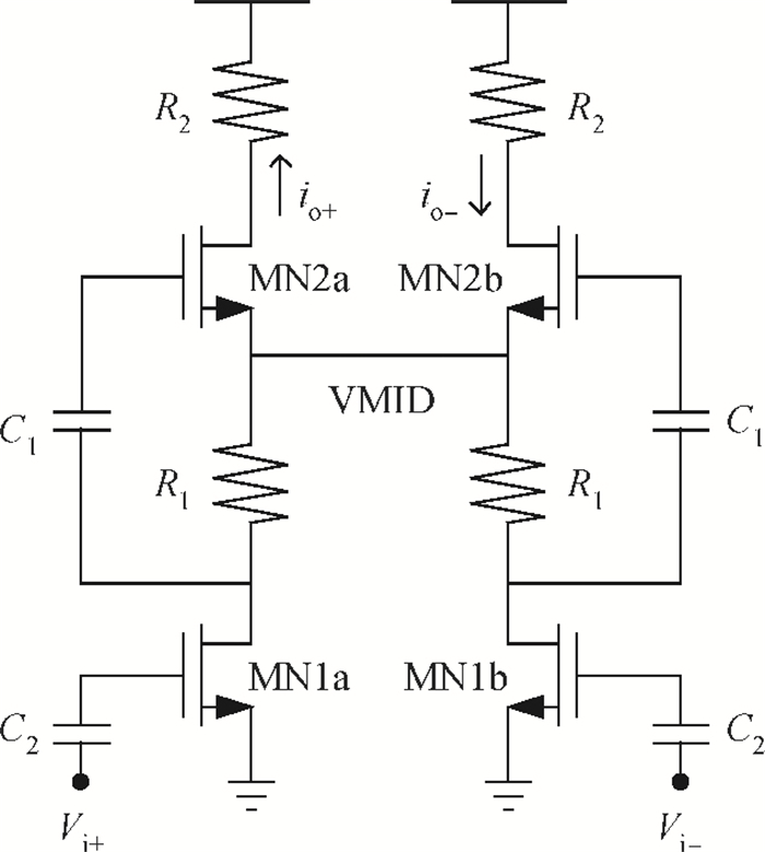
(a) Resistive-negative-feedback with follower. (b) Capacitor-cross-coupled common-gate LNA.
SEMICONDUCTOR INTEGRATED CIRCUITS
Yiou Jing and Huaxiang Lu
Corresponding author: Lu Huaxiang, luhx@semi.ac.cn
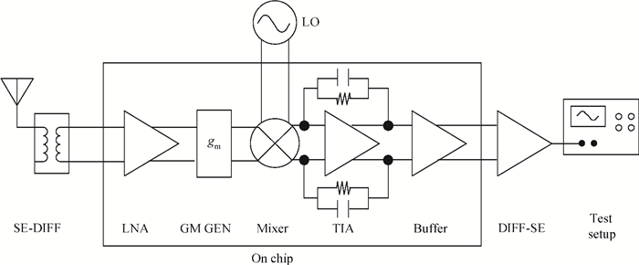
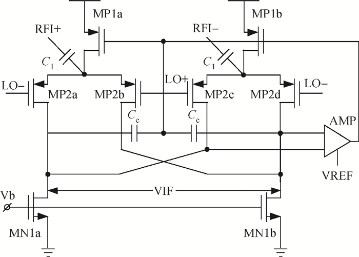
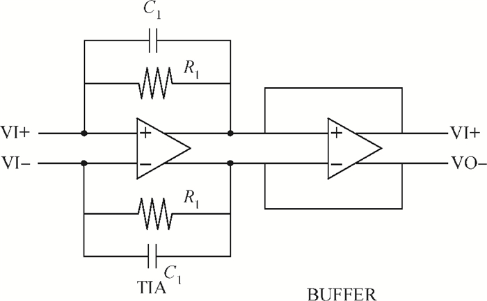
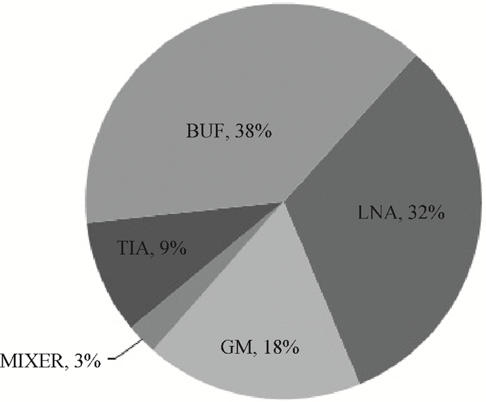
Abstract: This paper presents a wideband RF front-end with novel current-reuse wide band low noise amplifier (LNA), current-reuse V-I converter, active double balanced mixer and transimpedance amplifier for short range device (SRD) applications. With the proposed current-reuse LNA, the DC consumption of the front-end reduces considerably while maintaining sufficient performance needed by SRD devices. The RF front-end was fabricated in 0.18 μm RFCMOS process and occupies a silicon area of just 0.11 mm2. Operating in 433 MHz band, the measurement results show the RF front-end achieves a conversion gain of 29.7 dB, a double side band noise figure of 9.7 dB, an input referenced third intercept point of -24.9 dBm with only 1.44 mA power consumption from 1.8 V supply. Compared to other reported front-ends, it has an advantage in power consumption.
Keywords: low noise amplifier, mixer, RF front-end, short range device, common-gate, low power circuit
| [1] |
Okushima M, Borremans J, Linten D, et al. A DC-to-22 GHz 8.4 mW compact dual-feedback wideband LNA in 90 nm digital CMOS. IEEE Radio Frequency Integrated Circuits Symposium, 2009:295 http://ieeexplore.ieee.org/document/5135543/?reload=true&arnumber=5135543
|
| [2] |
Cicalini A, Aniruddhan S, Apte R, et al. A 65 nm CMOS SoC with embedded HSDPA/EDGE transceiver, digital baseband and multimedia processor. IEEE International Solid-State Circuits Conference Digest of Technical Papers (ISSCC), 2011:368 http://ieeexplore.ieee.org/document/5746357/
|
| [3] |
Van Langevelde R, van Elzakker M, van Goor D, et al. An ultra-low-power 868/915 MHz RF transceiver for wireless sensor network applications. IEEE Radio Frequency Integrated Circuits Symposium, 2009:113 http://ieeexplore.ieee.org/document/5135502/
|
| [4] |
Quinlan P, Crowley P, Chanca M, et al. A multimode 0.3-200 kb/s transceiver for the 433/868/915-MHz bands in 0.25-μm CMOS. IEEE J Solid-State Circuits, 2004, 39(12):2297 doi: 10.1109/JSSC.2004.836330
|
| [5] |
Wong A C W, Kathiresan G, Chan C K T, et al. A 1 V wireless transceiver for an ultra-low-power SoC for biotelemetry applications. IEEE J Solid-State Circuits, 2008, 43(7):1511 doi: 10.1109/JSSC.2008.923717
|
| [6] |
Belmas F, Hameau F, Fournier J. A 1.3 mW 20 dB gain low power inductorless LNA with 4 dB noise figure for 2.45 GHz ISM band. IEEE Radio Frequency Integrated Circuits Symposium (RFIC), 2011:1 http://ieeexplore.ieee.org/abstract/document/5940636/
|
| [7] |
Gong Zheng, Chen Bei, Hu Xueqing, et al. A low power 8th order elliptic low-pass filter for a CMMB tuner. Journal of Semiconductors, 2011, 32(9):095002 doi: 10.1088/1674-4926/32/9/095002
|
Table 1. Performance comparison to other works.

|
| [1] |
Okushima M, Borremans J, Linten D, et al. A DC-to-22 GHz 8.4 mW compact dual-feedback wideband LNA in 90 nm digital CMOS. IEEE Radio Frequency Integrated Circuits Symposium, 2009:295 http://ieeexplore.ieee.org/document/5135543/?reload=true&arnumber=5135543
|
| [2] |
Cicalini A, Aniruddhan S, Apte R, et al. A 65 nm CMOS SoC with embedded HSDPA/EDGE transceiver, digital baseband and multimedia processor. IEEE International Solid-State Circuits Conference Digest of Technical Papers (ISSCC), 2011:368 http://ieeexplore.ieee.org/document/5746357/
|
| [3] |
Van Langevelde R, van Elzakker M, van Goor D, et al. An ultra-low-power 868/915 MHz RF transceiver for wireless sensor network applications. IEEE Radio Frequency Integrated Circuits Symposium, 2009:113 http://ieeexplore.ieee.org/document/5135502/
|
| [4] |
Quinlan P, Crowley P, Chanca M, et al. A multimode 0.3-200 kb/s transceiver for the 433/868/915-MHz bands in 0.25-μm CMOS. IEEE J Solid-State Circuits, 2004, 39(12):2297 doi: 10.1109/JSSC.2004.836330
|
| [5] |
Wong A C W, Kathiresan G, Chan C K T, et al. A 1 V wireless transceiver for an ultra-low-power SoC for biotelemetry applications. IEEE J Solid-State Circuits, 2008, 43(7):1511 doi: 10.1109/JSSC.2008.923717
|
| [6] |
Belmas F, Hameau F, Fournier J. A 1.3 mW 20 dB gain low power inductorless LNA with 4 dB noise figure for 2.45 GHz ISM band. IEEE Radio Frequency Integrated Circuits Symposium (RFIC), 2011:1 http://ieeexplore.ieee.org/abstract/document/5940636/
|
| [7] |
Gong Zheng, Chen Bei, Hu Xueqing, et al. A low power 8th order elliptic low-pass filter for a CMMB tuner. Journal of Semiconductors, 2011, 32(9):095002 doi: 10.1088/1674-4926/32/9/095002
|


Article views: 4300 Times PDF downloads: 114 Times Cited by: 0 Times
Received: 05 March 2013 Revised: 26 March 2013 Online: Published: 01 October 2013
| Citation: |
Yiou Jing, Huaxiang Lu. Design of a low-power 433/915-MHz RF front-end with a current-reuse common-gate LNA[J]. Journal of Semiconductors, 2013, 34(10): 105006. doi: 10.1088/1674-4926/34/10/105006
****
Y O Jing, H X Lu. Design of a low-power 433/915-MHz RF front-end with a current-reuse common-gate LNA[J]. J. Semicond., 2013, 34(10): 105006. doi: 10.1088/1674-4926/34/10/105006.

|
| [1] |
Okushima M, Borremans J, Linten D, et al. A DC-to-22 GHz 8.4 mW compact dual-feedback wideband LNA in 90 nm digital CMOS. IEEE Radio Frequency Integrated Circuits Symposium, 2009:295 http://ieeexplore.ieee.org/document/5135543/?reload=true&arnumber=5135543
|
| [2] |
Cicalini A, Aniruddhan S, Apte R, et al. A 65 nm CMOS SoC with embedded HSDPA/EDGE transceiver, digital baseband and multimedia processor. IEEE International Solid-State Circuits Conference Digest of Technical Papers (ISSCC), 2011:368 http://ieeexplore.ieee.org/document/5746357/
|
| [3] |
Van Langevelde R, van Elzakker M, van Goor D, et al. An ultra-low-power 868/915 MHz RF transceiver for wireless sensor network applications. IEEE Radio Frequency Integrated Circuits Symposium, 2009:113 http://ieeexplore.ieee.org/document/5135502/
|
| [4] |
Quinlan P, Crowley P, Chanca M, et al. A multimode 0.3-200 kb/s transceiver for the 433/868/915-MHz bands in 0.25-μm CMOS. IEEE J Solid-State Circuits, 2004, 39(12):2297 doi: 10.1109/JSSC.2004.836330
|
| [5] |
Wong A C W, Kathiresan G, Chan C K T, et al. A 1 V wireless transceiver for an ultra-low-power SoC for biotelemetry applications. IEEE J Solid-State Circuits, 2008, 43(7):1511 doi: 10.1109/JSSC.2008.923717
|
| [6] |
Belmas F, Hameau F, Fournier J. A 1.3 mW 20 dB gain low power inductorless LNA with 4 dB noise figure for 2.45 GHz ISM band. IEEE Radio Frequency Integrated Circuits Symposium (RFIC), 2011:1 http://ieeexplore.ieee.org/abstract/document/5940636/
|
| [7] |
Gong Zheng, Chen Bei, Hu Xueqing, et al. A low power 8th order elliptic low-pass filter for a CMMB tuner. Journal of Semiconductors, 2011, 32(9):095002 doi: 10.1088/1674-4926/32/9/095002
|

 WeChat ID
Journal of Semiconductors © 2017 All Rights Reserved 京ICP备05085259号-2

 DownLoad: