


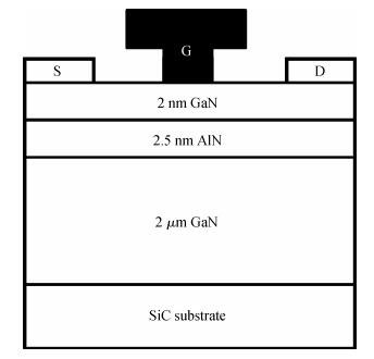
Fig. 1.
Schematic of the material structure of an AlN/GaN HEMT on an SiC substrate.
SEMICONDUCTOR DEVICES
Guodong Gu, Shaobo Dun, Yuanjie Lü, Tingting Han, Peng Xu, Jiayun Yin and Zhihong Feng
Corresponding author: Feng Zhihong, Email:blueledviet@yahoo.com.cn
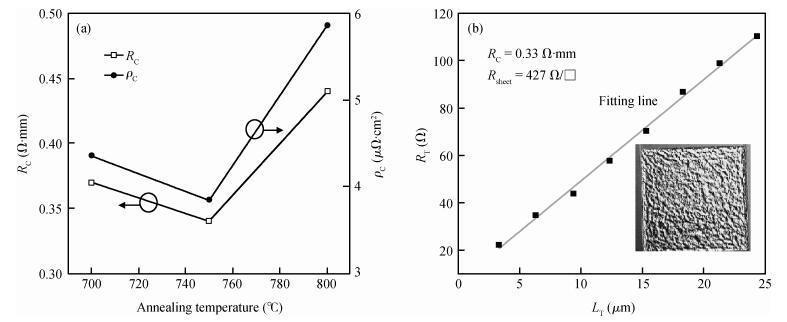
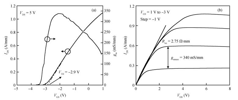
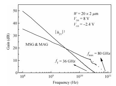
Abstract: AlN/GaN high-electron-mobility transistors (HEMTs) on SiC substrates were fabricated by metal-organic chemical vapor deposition (MOCVD) and then characterized. An Si/Ti/Al/Ni/Au stack was used to reduce ohmic contact resistance (0.33 Ω· mm) at a low annealing temperature. The fabricated devices exhibited a maximum drain current density of 1.07 A/mm (VGS=1 V) and a maximum peak extrinsic transconductance of 340 mS/mm. The off-state breakdown voltage of the device was 64 V with a gate-drain distance of 1.9 μm. The current gain extrinsic cutoff frequency fT and the maximum oscillation frequency fmax were 36 and 80 GHz with a 0.25 μm gate length, respectively.
Keywords: AlN/GaN HEMT, ohmic contact, SiC substrate, MOCVD
| [1] |
Micovic M, Kurdoghlian A, Hashimoto P, et al. GaN HFET for W-band power applications. IEDM Tech Dig, 2006:1
|
| [2] |
De Jaeger J C, Delage S L, Dambrine G, et al. Noise assessment of AlGaN/GaN HEMTs on Si or SiC substrates:application to X-band low noise amplifiers. European Gallium Arsenide and Other Semiconductor Application Symposium, EGAAS, 2005:229 http://core.ac.uk/display/11068817
|
| [3] |
Dabiran A M, Wowchak A M, Osinsky A, et al. Very high channel conductivity in low-defect AlN/GaN high electron mobility transistor structures. Appl Phys Lett, 2008, 93(8):082111 doi: 10.1063/1.2970991
|
| [4] |
Xing H G, Deen D, Cao Y, et al. PMBE-grown ultra-shallow AlN/GaN HFET technology. ECS Trans, 2007, 11(5):233 http://citeseerx.ist.psu.edu/viewdoc/summary?doi=10.1.1.712.3111
|
| [5] |
Cao Y, Jena D. High-mobility window for two-dimensional electron gases at ultrathin AlN/GaN heterojunctions. Appl Phys Lett, 2007, 90(18):182112 doi: 10.1063/1.2736207
|
| [6] |
Shinohara K, Regan D, Corrion A, et al. Deeply-scaled self-aligned-gate GaN DH-HEMTs with ultrahigh cut-off frequency. IEDM Tech Dig, 2011:457 http://www.mdpi.com/2079-9292/5/1/12/xml
|
| [7] |
Shinohara K, Regan D, Corrion A, et al. Self-aligned-gate GaN-HEMTs with heavily-doped n+-GaN ohmic contacts to 2DEG. IEDM Tech Dig, 2012:617 http://www-mtl.mit.edu/wpmu/ar2013/high-linearity-gan-hemts-with-nanowire-channel/
|
| [8] |
Medjdoub F, Zegaoui M, Waldhoff N, et al. Above 600 mS/mm transconductance with 2.3 A/mm drain current density AlN/GaN high-electron mobility transistors grown on silicon. Appl Phys Exp, 2011, 4(6):064106 doi: 10.1143/APEX.4.064106
|
| [9] |
Corrion A L, Shinohara K, Regan D, et al. High-speed AlN/GaN MOS-HFETs with scaled ALD Al2O3 gate insulators. IEEE Electron Device Lett, 2011, 32(8):1062 doi: 10.1109/LED.2011.2155616
|
| [10] |
Chabak K D, Walker D E, Johnson M R, et al. High-performance AlN/GaN HEMTs on sapphire substrate with an oxidized gate insulator. IEEE Electron Device Lett, 2011, 32(11):1677 http://adsabs.harvard.edu/abs/2011IEDL...32.1677C
|
| [11] |
Kim D W, Baik H K. Current conduction mechanism of Si/Ti-based ohmic contacts to n-GaN. Appl Phys Lett, 2000, 77(7):1011 doi: 10.1063/1.1289057
|
| [12] |
Lin C F, Cheng H C, Chi G C, et al. Improved contact performance of GaN film using Si diffusion. Appl Phys Lett, 2000, 76(14):1878 doi: 10.1063/1.126198
|
| [13] |
Mohammed F M, Wang L, Adesidaa I. First-layer Si metallizations for thermally stable and smooth ohmic contacts for AlGaN/GaN high electron mobility transistors. J Vac Sci Technol B, 2007, 25(2):324 doi: 10.1116/1.2437161
|


Article views: 5370 Times PDF downloads: 56 Times Cited by: 0 Times
Received: 29 March 2013 Revised: 23 April 2013 Online: Published: 01 November 2013
| Citation: |
Guodong Gu, Shaobo Dun, Yuanjie Lü, Tingting Han, Peng Xu, Jiayun Yin, Zhihong Feng. Low ohmic contact AlN/GaN HEMTs grown by MOCVD[J]. Journal of Semiconductors, 2013, 34(11): 114004. doi: 10.1088/1674-4926/34/11/114004
****
G D Gu, S B Dun, Y Lü, T T Han, P Xu, J Y Yin, Z H Feng. Low ohmic contact AlN/GaN HEMTs grown by MOCVD[J]. J. Semicond., 2013, 34(11): 114004. doi: 10.1088/1674-4926/34/11/114004.

|
| [1] |
Micovic M, Kurdoghlian A, Hashimoto P, et al. GaN HFET for W-band power applications. IEDM Tech Dig, 2006:1
|
| [2] |
De Jaeger J C, Delage S L, Dambrine G, et al. Noise assessment of AlGaN/GaN HEMTs on Si or SiC substrates:application to X-band low noise amplifiers. European Gallium Arsenide and Other Semiconductor Application Symposium, EGAAS, 2005:229 http://core.ac.uk/display/11068817
|
| [3] |
Dabiran A M, Wowchak A M, Osinsky A, et al. Very high channel conductivity in low-defect AlN/GaN high electron mobility transistor structures. Appl Phys Lett, 2008, 93(8):082111 doi: 10.1063/1.2970991
|
| [4] |
Xing H G, Deen D, Cao Y, et al. PMBE-grown ultra-shallow AlN/GaN HFET technology. ECS Trans, 2007, 11(5):233 http://citeseerx.ist.psu.edu/viewdoc/summary?doi=10.1.1.712.3111
|
| [5] |
Cao Y, Jena D. High-mobility window for two-dimensional electron gases at ultrathin AlN/GaN heterojunctions. Appl Phys Lett, 2007, 90(18):182112 doi: 10.1063/1.2736207
|
| [6] |
Shinohara K, Regan D, Corrion A, et al. Deeply-scaled self-aligned-gate GaN DH-HEMTs with ultrahigh cut-off frequency. IEDM Tech Dig, 2011:457 http://www.mdpi.com/2079-9292/5/1/12/xml
|
| [7] |
Shinohara K, Regan D, Corrion A, et al. Self-aligned-gate GaN-HEMTs with heavily-doped n+-GaN ohmic contacts to 2DEG. IEDM Tech Dig, 2012:617 http://www-mtl.mit.edu/wpmu/ar2013/high-linearity-gan-hemts-with-nanowire-channel/
|
| [8] |
Medjdoub F, Zegaoui M, Waldhoff N, et al. Above 600 mS/mm transconductance with 2.3 A/mm drain current density AlN/GaN high-electron mobility transistors grown on silicon. Appl Phys Exp, 2011, 4(6):064106 doi: 10.1143/APEX.4.064106
|
| [9] |
Corrion A L, Shinohara K, Regan D, et al. High-speed AlN/GaN MOS-HFETs with scaled ALD Al2O3 gate insulators. IEEE Electron Device Lett, 2011, 32(8):1062 doi: 10.1109/LED.2011.2155616
|
| [10] |
Chabak K D, Walker D E, Johnson M R, et al. High-performance AlN/GaN HEMTs on sapphire substrate with an oxidized gate insulator. IEEE Electron Device Lett, 2011, 32(11):1677 http://adsabs.harvard.edu/abs/2011IEDL...32.1677C
|
| [11] |
Kim D W, Baik H K. Current conduction mechanism of Si/Ti-based ohmic contacts to n-GaN. Appl Phys Lett, 2000, 77(7):1011 doi: 10.1063/1.1289057
|
| [12] |
Lin C F, Cheng H C, Chi G C, et al. Improved contact performance of GaN film using Si diffusion. Appl Phys Lett, 2000, 76(14):1878 doi: 10.1063/1.126198
|
| [13] |
Mohammed F M, Wang L, Adesidaa I. First-layer Si metallizations for thermally stable and smooth ohmic contacts for AlGaN/GaN high electron mobility transistors. J Vac Sci Technol B, 2007, 25(2):324 doi: 10.1116/1.2437161
|

 WeChat ID
Journal of Semiconductors © 2017 All Rights Reserved 京ICP备05085259号-2

 DownLoad:

