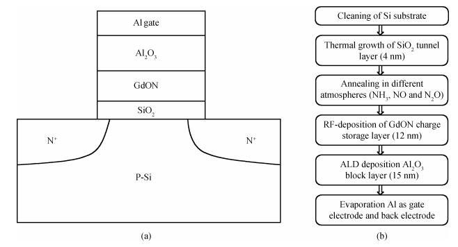
Fig. 1.
(a) Cross-section diagram, and (b) brief process flow of MONOS capacitors
SEMICONDUCTOR DEVICES
Meilin He, Jingping Xu, Jianxiong Chen and Lu Liu
Corresponding author: Xu Jingping, Email:jpxu@mail.hust.edu.cn
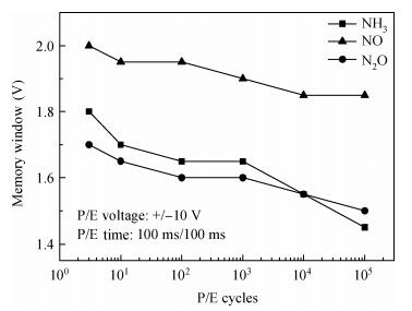
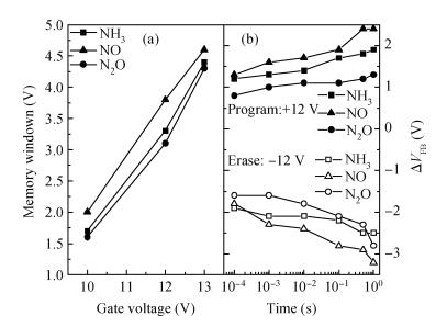
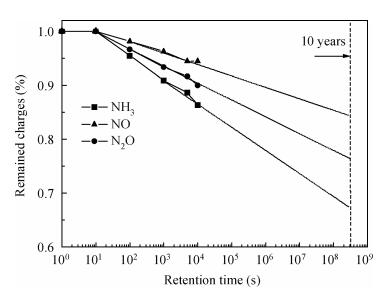
Abstract: Metal-oxide-nitride-oxide-silicon (MONOS) capacitors with thermally grown SiO2 as the tunnel layer are fabricated, and the effects of different ambient nitridation (NH3, NO and N2O) on the characteristics of the memory capacitors are investigated. The experimental results indicate that the device with tunnel oxide annealed in NO ambient exhibits excellent memory characteristics, i.e. a large memory window, high program/erase speed, and good endurance and retention performance (the charge loss rate is 14.5% after 10 years). The mechanism involved is that much more nitrogen is incorporated into the tunnel oxide during NO annealing, resulting in a lower tunneling barrier height and smaller interface state density. Thus, there is a higher tunneling rate under a high electric field and a lower probability of trap-assisted tunneling during retention, as compared to N2O annealing. Furthermore, compared with the NH3-annealed device, no weak Si-H bonds and electron traps related to the hydrogen are introduced for the NO-annealed devices, giving a high-quality and high-reliability SiON tunneling layer and SiON/Si interface due to the suitable nitridation and oxidation roles of NO.
Keywords: MONOS memory, memory characteristics, annealing, nitridation
| [1] |
Sun L, Pang H Q, Pan L Y, et al. An improved charge pumping method to study distribution of trapped charges in SONOS memory. Chinese Journal of Semiconductors, 2005, 25(10):1886
|
| [2] |
Liao J H, Hsieh J Y, Lue H T, et al. Performance and reliability optimizations of BE-SONOS NAND flash using SiON bandgap-tuning tunneling barrier. IEEE International Conference of Reliability Physics Symposium (IPRS), 2010:639
|
| [3] |
Wang X G, Liu J, Bai W P, et al. A novel MONOS-type nonvolatile memory using high-k dielectrics for improved data retention and programming speed. IEEE Trans Electron Devices, 2004, 51(4):597 doi: 10.1109/TED.2004.824684
|
| [4] |
Jin R, Liu X Y, Du G, et al. Effect of trapped charge accumulation on the retention of charge trapping memory. Journal of Semiconductors, 2010, 31(12):124016 doi: 10.1088/1674-4926/31/12/124016
|
| [5] |
Bu J K, White H M. Improvement in retention reliability of SONOS nonvolatile memory devices by two-step high temperature deuterium anneal. 39th IEEE Annual International Reliability Physics Symposium, 2001:52
|
| [6] |
Guarini T, Bevan M, Ripley M, et al. Nitric oxide rapid thermal nitridation for flash memory applications. 18th International Conference on Advanced Thermal Processing of Semiconductors (RTP), 2010:166
|
| [7] |
Fukuda H, Uchiyama A, Kuramochi T, et al. High-performance scaled flash-type EEPROMs with heavily oxynitrided tunnel oxide film. International Conference of Electron Devices Meeting, 1992:465
|
| [8] |
Wu J L, Chien H C, Liao C W, et al. Comparison of electrical and reliability characteristics of different tunnel oxides in SONOS flash memory. IEEE International Workshop on Memory Technology, Design, and Testing, 2006:4
|
| [9] |
Xu J P, Lai P T, Cheng Y C. Gate dielectrics prepared by double nitridation in NO and N2O. Appl Phys A, 2000, 70(1):101 doi: 10.1007/s003390050020
|
| [10] |
Ganguly U, Guarini T, Wellekens D, et al. Impact of top-surface tunnel-oxide nitridation on flash memory performance and reliability. IEEE Electron Device Lett, 2010, 31(2):123 doi: 10.1109/LED.2009.2036577
|
| [11] |
Habermehl S, Nasby R D, Rightley M J. Cycling endurance of silicon-oxide-nitride-oxide-silicon nonvolatile memory stacks prepared with nitrided SiO2/Si (100) interfaces. Appl Phys Lett, 1999, 75(8):1122 doi: 10.1063/1.124616
|
| [12] |
Lu H C, Gusev E P, Garfunkel E, et al. Isotopic labeling studies of interactions of nitric oxide and nitrous oxide with ultrathin oxynitride layers on silicon. J Appl Phys, 2000, 87(3):1550 doi: 10.1063/1.372048
|
| [13] |
Soleimani H R, Philipossian A, Doyle B S. A study of the growth kinetics of SiO2 in N2O for MOSFETs. International Electron Devices Meeting, 1992:629
|
| [14] |
Wu J L, Kao C C, Chien H C, et al. Retention reliability improvement of SONOS non-volatile memory with N2O oxidation tunnel oxide. IEEE International Integrated Reliability Workshop Final Report, 2006:209
|
| [15] |
Ji F, Xu J P, Zhang H Q, et al. Influence of natridation annealing of HfTiO on electrical properties of MOS device. Research & Progress of Solid State Electronics, 2008, 28(3):330 http://en.cnki.com.cn/Article_en/CJFDTOTAL-GTDZ200803005.htm
|
| [16] |
Yao Z Q, Harrison H B, Dimitrijev S, et al. Effects of nitric oxide annealing of thermally grown silicon dioxide characteristics. IEEE Electron Device Lett, 1995, 16(8):345 doi: 10.1109/55.400733
|
| [17] |
Bhat M, Kim J, Yoon G W, et al. MOS characteristics of ultrathin no-grown oxynitrides. IEEE Electron Device Lett, 1994, 15(10):421 doi: 10.1109/55.320988
|


Article views: 3750 Times PDF downloads: 33 Times Cited by: 0 Times
Received: 29 March 2013 Revised: 13 May 2013 Online: Published: 01 November 2013
| Citation: |
Meilin He, Jingping Xu, Jianxiong Chen, Lu Liu. Improved memory performance of metal-oxide-nitride-oxide-silicon by annealing the SiO2 tunnel layer in different nitridation atmospheres[J]. Journal of Semiconductors, 2013, 34(11): 114005. doi: 10.1088/1674-4926/34/11/114005
****
M L He, J P Xu, J X Chen, L Liu. Improved memory performance of metal-oxide-nitride-oxide-silicon by annealing the SiO2 tunnel layer in different nitridation atmospheres[J]. J. Semicond., 2013, 34(11): 114005. doi: 10.1088/1674-4926/34/11/114005.

|
| [1] |
Sun L, Pang H Q, Pan L Y, et al. An improved charge pumping method to study distribution of trapped charges in SONOS memory. Chinese Journal of Semiconductors, 2005, 25(10):1886
|
| [2] |
Liao J H, Hsieh J Y, Lue H T, et al. Performance and reliability optimizations of BE-SONOS NAND flash using SiON bandgap-tuning tunneling barrier. IEEE International Conference of Reliability Physics Symposium (IPRS), 2010:639
|
| [3] |
Wang X G, Liu J, Bai W P, et al. A novel MONOS-type nonvolatile memory using high-k dielectrics for improved data retention and programming speed. IEEE Trans Electron Devices, 2004, 51(4):597 doi: 10.1109/TED.2004.824684
|
| [4] |
Jin R, Liu X Y, Du G, et al. Effect of trapped charge accumulation on the retention of charge trapping memory. Journal of Semiconductors, 2010, 31(12):124016 doi: 10.1088/1674-4926/31/12/124016
|
| [5] |
Bu J K, White H M. Improvement in retention reliability of SONOS nonvolatile memory devices by two-step high temperature deuterium anneal. 39th IEEE Annual International Reliability Physics Symposium, 2001:52
|
| [6] |
Guarini T, Bevan M, Ripley M, et al. Nitric oxide rapid thermal nitridation for flash memory applications. 18th International Conference on Advanced Thermal Processing of Semiconductors (RTP), 2010:166
|
| [7] |
Fukuda H, Uchiyama A, Kuramochi T, et al. High-performance scaled flash-type EEPROMs with heavily oxynitrided tunnel oxide film. International Conference of Electron Devices Meeting, 1992:465
|
| [8] |
Wu J L, Chien H C, Liao C W, et al. Comparison of electrical and reliability characteristics of different tunnel oxides in SONOS flash memory. IEEE International Workshop on Memory Technology, Design, and Testing, 2006:4
|
| [9] |
Xu J P, Lai P T, Cheng Y C. Gate dielectrics prepared by double nitridation in NO and N2O. Appl Phys A, 2000, 70(1):101 doi: 10.1007/s003390050020
|
| [10] |
Ganguly U, Guarini T, Wellekens D, et al. Impact of top-surface tunnel-oxide nitridation on flash memory performance and reliability. IEEE Electron Device Lett, 2010, 31(2):123 doi: 10.1109/LED.2009.2036577
|
| [11] |
Habermehl S, Nasby R D, Rightley M J. Cycling endurance of silicon-oxide-nitride-oxide-silicon nonvolatile memory stacks prepared with nitrided SiO2/Si (100) interfaces. Appl Phys Lett, 1999, 75(8):1122 doi: 10.1063/1.124616
|
| [12] |
Lu H C, Gusev E P, Garfunkel E, et al. Isotopic labeling studies of interactions of nitric oxide and nitrous oxide with ultrathin oxynitride layers on silicon. J Appl Phys, 2000, 87(3):1550 doi: 10.1063/1.372048
|
| [13] |
Soleimani H R, Philipossian A, Doyle B S. A study of the growth kinetics of SiO2 in N2O for MOSFETs. International Electron Devices Meeting, 1992:629
|
| [14] |
Wu J L, Kao C C, Chien H C, et al. Retention reliability improvement of SONOS non-volatile memory with N2O oxidation tunnel oxide. IEEE International Integrated Reliability Workshop Final Report, 2006:209
|
| [15] |
Ji F, Xu J P, Zhang H Q, et al. Influence of natridation annealing of HfTiO on electrical properties of MOS device. Research & Progress of Solid State Electronics, 2008, 28(3):330 http://en.cnki.com.cn/Article_en/CJFDTOTAL-GTDZ200803005.htm
|
| [16] |
Yao Z Q, Harrison H B, Dimitrijev S, et al. Effects of nitric oxide annealing of thermally grown silicon dioxide characteristics. IEEE Electron Device Lett, 1995, 16(8):345 doi: 10.1109/55.400733
|
| [17] |
Bhat M, Kim J, Yoon G W, et al. MOS characteristics of ultrathin no-grown oxynitrides. IEEE Electron Device Lett, 1994, 15(10):421 doi: 10.1109/55.320988
|

 WeChat ID
Journal of Semiconductors © 2017 All Rights Reserved 京ICP备05085259号-2

 DownLoad: