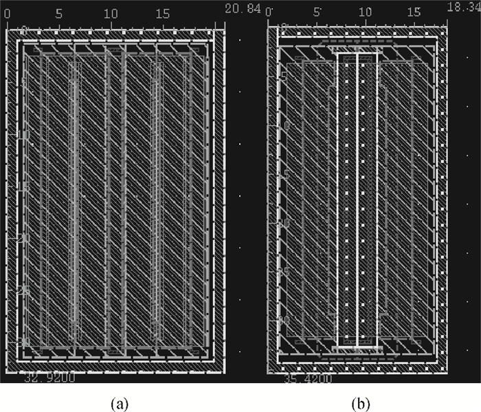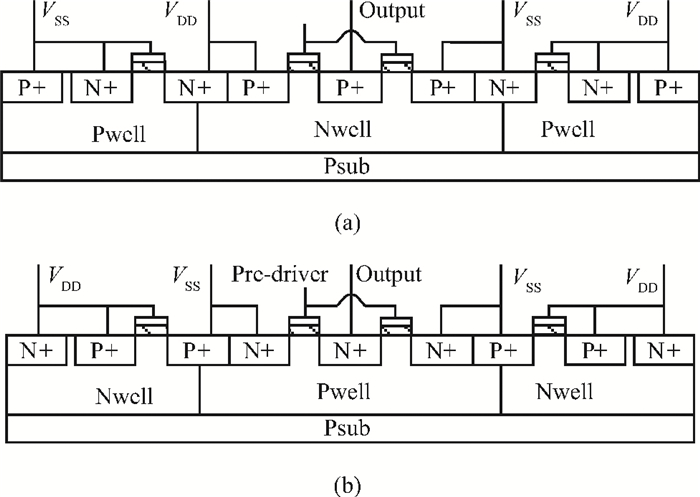
Fig. 1.
The proposed structure composed of (a) device A, and (b) device B.
SEMICONDUCTOR DEVICES
Hang Fan, Lingli Jiang and Bo Zhang
Corresponding author: Fan Hang, fanmes@163.com
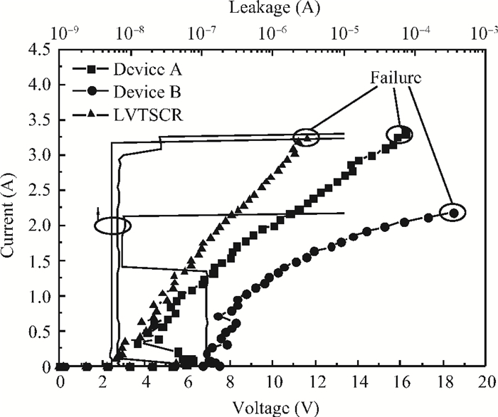
Abstract: Electro-static discharge (ESD) is always a serious threat to integrated circuits. To achieve higher robustness and a smaller die area at the same time, a novel protection structure for the output pad is proposed. The complementary SCR devices in this structure can protect not only the output under positive or negative stresses versus VDD or VSS, respectively, but also the power rails at the cost of almost no extra area. The robustness of the proposed structure is about three times higher than the conventional four-finger GGNMOS/GDPMOS structure in the same area condition.
Keywords: electro-static discharge, power clamp, silicon controlled rectifier
| [1] |
Song B, Han Y, Li M, et al. Substrate-triggered GGNMOS in 65 nm CMOS process for ESD application. Electron Lett, 2010, 46(7):518 doi: 10.1049/el.2010.0205
|
| [2] |
Lee J H, Shih J R, Yang D H, et al. A simple solution for low-driving-current output buffer failed at the low voltage ESD zapping event. International Symp Physical and Failure Analysis of Integrated Circuits (IPFA), 2012 http://ieeexplore.ieee.org/document/6306259/authors
|
| [3] |
Ker M D, Chen W Y, Shieh W T, et al. New ballasting layout schemes to improve ESD robustness of I/O buffers in fully silicided CMOS process. Symp EOS/ESD Symposium, 2009:1 http://ieeexplore.ieee.org/document/5299049/keywords
|
| [4] |
Yeh C T, Ker M D. Capacitor-less design of power-rail ESD clamp circuit with adjustable holding voltage for on-chip ESD protection. IEEE J Solid-State Circuits, 2010, 45(11):2476 https://www.infona.pl/resource/bwmeta1.element.ieee-art-000005597958
|
| [5] |
Amerasekera A, Duvvury C. ESD in silicon integrated circuits. 2nd ed. England:John Wiley & Sons, Ltd., 2002:150
|
| [6] |
Amerasekera A, Duvvury C. ESD in silicon integrated circuits. 2nd ed. England:John Wiley & Sons, Ltd., 2002:256
|
| [7] |
Chen T Y, Ker M D. Investigation of the gate-driven effect and substrate-triggered effect on ESD robustness of CMOS devices. IEEE Trans Device Mater Reliab, 2001, 1(4):190 doi: 10.1109/7298.995833
|
| [8] |
Wang G C, Chen C H, Huang W H, et al. Gate-driven 3.3 V ESD clamp using 1.8 V transistors. International Conf IC Design & Technology (ICICDT), 2011
|
| [9] |
Wang C T, Ker M D. Design of 2×VDD-tolerant power-rail ESD clamp circuit with consideration of gate leakage current in 65-nm CMOS technology. Electron Devices, 2010, 57(6):1460 doi: 10.1109/TED.2010.2046457
|
| [10] |
Amerasekera A, Duvvury C. ESD in silicon integrated circuits. 2nd ed. England:John Wiley & Sons, Ltd., 2002:98
|
| [11] |
Ker M D, Chen J H. Self-substrate-triggered technique to enhance turn-on uniformity of multi-finger ESD protection devices. IEEE J Solid-State Circuits, 2006, 41:2601 doi: 10.1109/JSSC.2006.883331
|
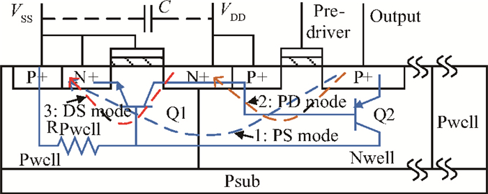
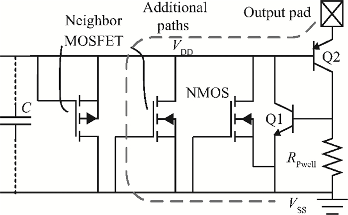
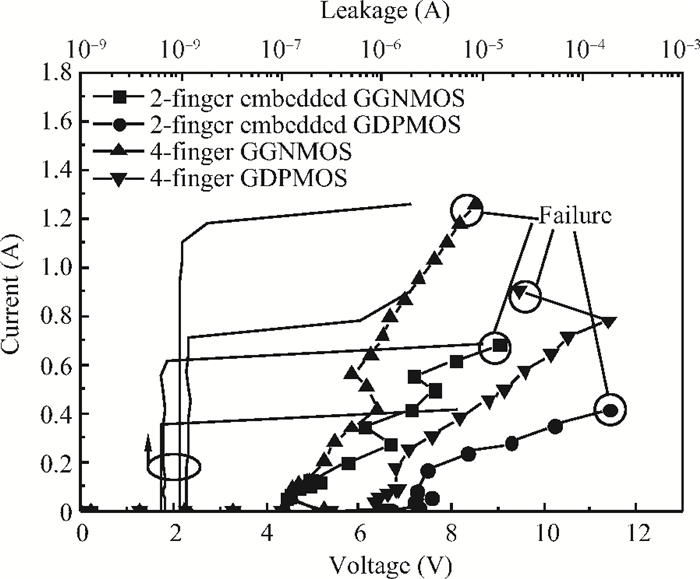
Table 1. The ESD characteristics of devices A, B and the conventional MOSFET.

|
| [1] |
Song B, Han Y, Li M, et al. Substrate-triggered GGNMOS in 65 nm CMOS process for ESD application. Electron Lett, 2010, 46(7):518 doi: 10.1049/el.2010.0205
|
| [2] |
Lee J H, Shih J R, Yang D H, et al. A simple solution for low-driving-current output buffer failed at the low voltage ESD zapping event. International Symp Physical and Failure Analysis of Integrated Circuits (IPFA), 2012 http://ieeexplore.ieee.org/document/6306259/authors
|
| [3] |
Ker M D, Chen W Y, Shieh W T, et al. New ballasting layout schemes to improve ESD robustness of I/O buffers in fully silicided CMOS process. Symp EOS/ESD Symposium, 2009:1 http://ieeexplore.ieee.org/document/5299049/keywords
|
| [4] |
Yeh C T, Ker M D. Capacitor-less design of power-rail ESD clamp circuit with adjustable holding voltage for on-chip ESD protection. IEEE J Solid-State Circuits, 2010, 45(11):2476 https://www.infona.pl/resource/bwmeta1.element.ieee-art-000005597958
|
| [5] |
Amerasekera A, Duvvury C. ESD in silicon integrated circuits. 2nd ed. England:John Wiley & Sons, Ltd., 2002:150
|
| [6] |
Amerasekera A, Duvvury C. ESD in silicon integrated circuits. 2nd ed. England:John Wiley & Sons, Ltd., 2002:256
|
| [7] |
Chen T Y, Ker M D. Investigation of the gate-driven effect and substrate-triggered effect on ESD robustness of CMOS devices. IEEE Trans Device Mater Reliab, 2001, 1(4):190 doi: 10.1109/7298.995833
|
| [8] |
Wang G C, Chen C H, Huang W H, et al. Gate-driven 3.3 V ESD clamp using 1.8 V transistors. International Conf IC Design & Technology (ICICDT), 2011
|
| [9] |
Wang C T, Ker M D. Design of 2×VDD-tolerant power-rail ESD clamp circuit with consideration of gate leakage current in 65-nm CMOS technology. Electron Devices, 2010, 57(6):1460 doi: 10.1109/TED.2010.2046457
|
| [10] |
Amerasekera A, Duvvury C. ESD in silicon integrated circuits. 2nd ed. England:John Wiley & Sons, Ltd., 2002:98
|
| [11] |
Ker M D, Chen J H. Self-substrate-triggered technique to enhance turn-on uniformity of multi-finger ESD protection devices. IEEE J Solid-State Circuits, 2006, 41:2601 doi: 10.1109/JSSC.2006.883331
|


Article views: 3289 Times PDF downloads: 28 Times Cited by: 0 Times
Received: 01 April 2013 Revised: 16 May 2013 Online: Published: 01 November 2013
| Citation: |
Hang Fan, Lingli Jiang, Bo Zhang. A novel ESD protection structure for output pads[J]. Journal of Semiconductors, 2013, 34(11): 114016. doi: 10.1088/1674-4926/34/11/114016
****
H Fan, L L Jiang, B Zhang. A novel ESD protection structure for output pads[J]. J. Semicond., 2013, 34(11): 114016. doi: 10.1088/1674-4926/34/11/114016.

|
| [1] |
Song B, Han Y, Li M, et al. Substrate-triggered GGNMOS in 65 nm CMOS process for ESD application. Electron Lett, 2010, 46(7):518 doi: 10.1049/el.2010.0205
|
| [2] |
Lee J H, Shih J R, Yang D H, et al. A simple solution for low-driving-current output buffer failed at the low voltage ESD zapping event. International Symp Physical and Failure Analysis of Integrated Circuits (IPFA), 2012 http://ieeexplore.ieee.org/document/6306259/authors
|
| [3] |
Ker M D, Chen W Y, Shieh W T, et al. New ballasting layout schemes to improve ESD robustness of I/O buffers in fully silicided CMOS process. Symp EOS/ESD Symposium, 2009:1 http://ieeexplore.ieee.org/document/5299049/keywords
|
| [4] |
Yeh C T, Ker M D. Capacitor-less design of power-rail ESD clamp circuit with adjustable holding voltage for on-chip ESD protection. IEEE J Solid-State Circuits, 2010, 45(11):2476 https://www.infona.pl/resource/bwmeta1.element.ieee-art-000005597958
|
| [5] |
Amerasekera A, Duvvury C. ESD in silicon integrated circuits. 2nd ed. England:John Wiley & Sons, Ltd., 2002:150
|
| [6] |
Amerasekera A, Duvvury C. ESD in silicon integrated circuits. 2nd ed. England:John Wiley & Sons, Ltd., 2002:256
|
| [7] |
Chen T Y, Ker M D. Investigation of the gate-driven effect and substrate-triggered effect on ESD robustness of CMOS devices. IEEE Trans Device Mater Reliab, 2001, 1(4):190 doi: 10.1109/7298.995833
|
| [8] |
Wang G C, Chen C H, Huang W H, et al. Gate-driven 3.3 V ESD clamp using 1.8 V transistors. International Conf IC Design & Technology (ICICDT), 2011
|
| [9] |
Wang C T, Ker M D. Design of 2×VDD-tolerant power-rail ESD clamp circuit with consideration of gate leakage current in 65-nm CMOS technology. Electron Devices, 2010, 57(6):1460 doi: 10.1109/TED.2010.2046457
|
| [10] |
Amerasekera A, Duvvury C. ESD in silicon integrated circuits. 2nd ed. England:John Wiley & Sons, Ltd., 2002:98
|
| [11] |
Ker M D, Chen J H. Self-substrate-triggered technique to enhance turn-on uniformity of multi-finger ESD protection devices. IEEE J Solid-State Circuits, 2006, 41:2601 doi: 10.1109/JSSC.2006.883331
|

 WeChat ID
Journal of Semiconductors © 2017 All Rights Reserved 京ICP备05085259号-2

 DownLoad: