


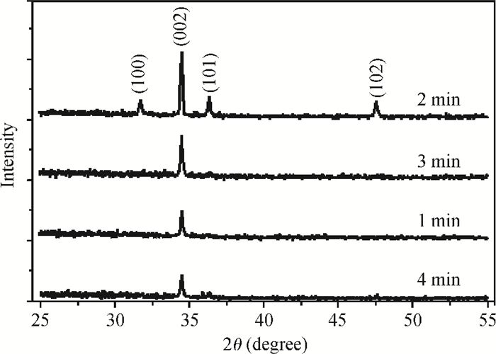
Fig. 1.
X-ray diffraction spectra of ZnO thin films grown at various times, the films deposited on glass substrate at Ts D 350 ℃.
SEMICONDUCTOR MATERIALS
Said Benramache1, Foued Chabane2, Boubaker Benhaoua3 and Fatima Z. Lemmadi2
Corresponding author: Said Benramache, benramache.said@gmail.com
Abstract: This paper examines the growth of ZnO thin films on glass substrate at 350℃ using an ultrasonic spray technique. We have investigated the influence of growth time ranging from 1 to 4 min on structural, optical and electrical properties of ZnO thin films. The as-grown films exhibit a hexagonal structure wurtzite and are (002) oriented. The maximum value of grain size G=63.99 nm is attained for ZnO films grown at 2 min. The average transmittance is about 80%, thus the films are transparent in the visible region. The optical gap energy is found to increase from 3.26 to 3.37 eV with growth time increased from 1 to 2 min. The minimum value of electrical resistivity of the films is 0.13 Ω·cm obtained at 2 min. A systematic study on the influence of growth time on the properties of ZnO thin films deposited by ultrasonic spray at 350℃ has been reported.
Keywords: ZnO, thin film, growth time, ultrasonic spray technique
| [1] |
Zhang Y, Wu C, Zheng Y, et al. Synthesis and efficient field emission characteristics of patterned ZnO nanowires. Journal of Semiconductors, 2012, 33(2):023001 doi: 10.1088/1674-4926/33/2/023001
|
| [2] |
Wu Y, Zhang L, Xie G, et al. Structural and electrical properties of (110) ZnO epitaxial thin films on (001) SrTiO3 substrates. Solid State Commun, 2008, 148(2):247
|
| [3] |
Zhang H, Liu H, Lei C, et al. Low-temperature deposition of transparent conducting Mn-W co-doped ZnO thin films. Journal of Semiconductors, 2010, 31(8):083005 doi: 10.1088/1674-4926/31/8/083005
|
| [4] |
Ji Z, Mao Q, Ke W. Effects of oxygen partial pressure on resistive switching characteristics of ZnO thin films by DC reactive magnetron sputtering. Solid State Commun, 2010, 150(8):1919 http://cat.inist.fr/?aModele=afficheN&cpsidt=23242033
|
| [5] |
Li W J, Kong C Y, Ruan H B, et al. Electrical properties and Raman scattering investigation of Ag doped ZnO thin films. Solid State Commun, 2012, 152(2):147 doi: 10.1016/j.ssc.2011.10.006
|
| [6] |
Ye Z, Yuan G, Li B, et al. Fabrication and characteristics of ZnO thin films with Al/Si (100) substrates. Mater Chem Phys, 2005, 93(2):170
|
| [7] |
Meng X, Lin B, Gu B, et al. A simple growth route towards ZnO thin films and nanorods. Solid State Commun, 2005, 135(3):411 http://cat.inist.fr/?aModele=afficheN&cpsidt=16972517
|
| [8] |
El Manouni A, Manjon F J, Perales M, et al. Effect of thermal annealing on ZnO:Al thin films grown by spray pyrolysis. Superlattices and Microstructures, 2007, 42(2):134 http://personales.upv.es/~fjmanjon/sm42_134.pdf
|
| [9] |
Benramache S, Benhaoua B, Chabane F. Effect of substrate temperature on the stability of transparent conducting cobalt doped ZnO thin films. Journal of Semiconductors, 2012, 33(9):093001 doi: 10.1088/1674-4926/33/9/093001
|
| [10] |
Vernardou D, Kenanakis G, Couris S, et al. The effect of growth time on the morphology of ZnO structures deposited on Si (100) by the aqueous chemical growth technique. J Cryst Growth, 2007, 308(2):105
|
| [11] |
Mekhanache M, Drici A, Hamideche L S, et al. Properties of ZnO thin films deposited on (glass, ITO and ZnO:Al) substrates. Superl Micros, 2011, 49(3):510 http://adsabs.harvard.edu/abs/2011SuMi...49..510M
|
| [12] |
Zhang C. High-quality oriented ZnO films grown by sol-gel process assisted with ZnO. Journal of Physics and Chemistry of Solids, 2010, 71(2):364
|
| [13] |
Nian H, Hahn S H, Koo K K, et al. Sol-gel derived N-doped ZnO thin films. Mater Lett, 2009, 63(10):2246 http://www.sciencedirect.com/science/article/pii/S0167577X09005631
|
| [14] |
Ben Ayadi Z, El Mir L, Djessas K, et al. Effect of the annealing temperature on transparency and conductivity of ZnO:Al thin films. Thin Solid Films, 2009, 517(22):6305 http://www.sciencedirect.com/science/article/pii/S0040609009003460
|
| [15] |
Wu S P, Zhao Q Y, Zheng L Q, et al. Behaviors of ZnO-doped silver thick film and silver grain growth mechanism. Solid State Sci, 2011, 13(3):548 doi: 10.1016/j.solidstatesciences.2010.12.024
|
| [16] |
Jain A, Sagar P, Mehra R M. Band gap widening and narrowing in moderately and heavily doped n-ZnO films. Solid-State Electron, 2006, 50(2):1420
|
| [17] |
Daranfed W, Aida M S, Hafdallah A, et al. Substrate temperature influence on ZnS thin films prepared by ultrasonic spray. Thin Solid Films, 2009, 518(3):1082 http://adsabs.harvard.edu/abs/2009TSF...518.1082D
|
| [18] |
Zhang D H, Yang T L, Ma J, et al. Preparation of transparent conducting ZnO:Al films on polymersubstrates by r. f. magnetron sputtering. Appl Surf Sci, 2000, 158(1):43
|
| [19] |
Hafdallah A, Yanineb F, Aida M S, et al. In doped ZnO thin films. Journal of Alloys and Compounds, 2011, 509(18):7267 http://www.sciencedirect.com/science/article/pii/S0925838811008954
|
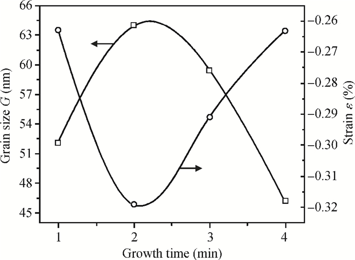
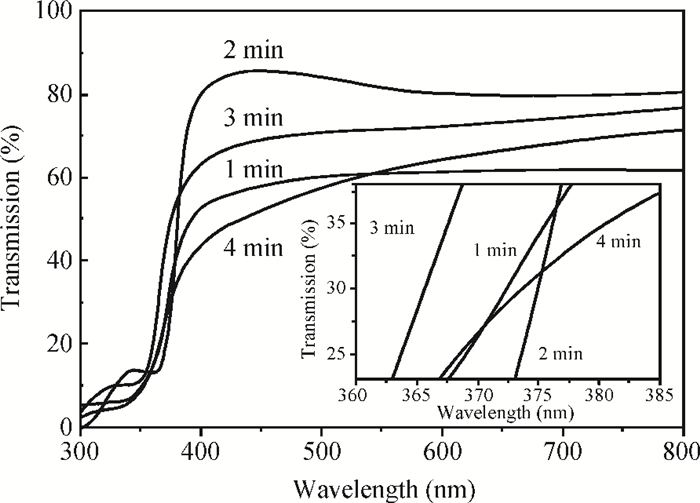
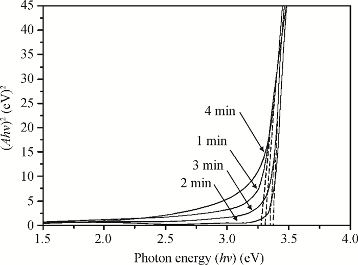
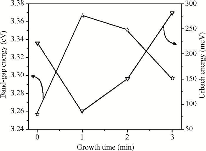
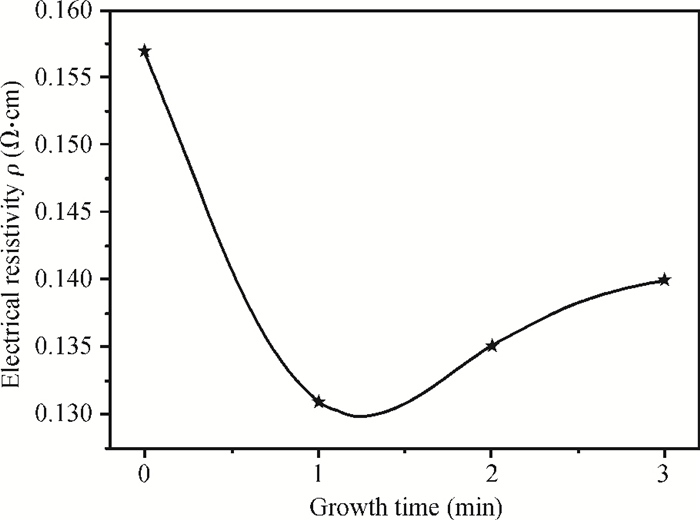
Table 1. Bragg angle 2$\theta $, the full width at half-maximum FWHM $\beta $, the grain size G, lattice parameters c and a, the strain$\varepsilon $ for (002) plane, band gap energy Eg, Urbach energy Eu and electrical resistivity $\rho $ for ZnO thin films were measured as a function of growth time.

|
| [1] |
Zhang Y, Wu C, Zheng Y, et al. Synthesis and efficient field emission characteristics of patterned ZnO nanowires. Journal of Semiconductors, 2012, 33(2):023001 doi: 10.1088/1674-4926/33/2/023001
|
| [2] |
Wu Y, Zhang L, Xie G, et al. Structural and electrical properties of (110) ZnO epitaxial thin films on (001) SrTiO3 substrates. Solid State Commun, 2008, 148(2):247
|
| [3] |
Zhang H, Liu H, Lei C, et al. Low-temperature deposition of transparent conducting Mn-W co-doped ZnO thin films. Journal of Semiconductors, 2010, 31(8):083005 doi: 10.1088/1674-4926/31/8/083005
|
| [4] |
Ji Z, Mao Q, Ke W. Effects of oxygen partial pressure on resistive switching characteristics of ZnO thin films by DC reactive magnetron sputtering. Solid State Commun, 2010, 150(8):1919 http://cat.inist.fr/?aModele=afficheN&cpsidt=23242033
|
| [5] |
Li W J, Kong C Y, Ruan H B, et al. Electrical properties and Raman scattering investigation of Ag doped ZnO thin films. Solid State Commun, 2012, 152(2):147 doi: 10.1016/j.ssc.2011.10.006
|
| [6] |
Ye Z, Yuan G, Li B, et al. Fabrication and characteristics of ZnO thin films with Al/Si (100) substrates. Mater Chem Phys, 2005, 93(2):170
|
| [7] |
Meng X, Lin B, Gu B, et al. A simple growth route towards ZnO thin films and nanorods. Solid State Commun, 2005, 135(3):411 http://cat.inist.fr/?aModele=afficheN&cpsidt=16972517
|
| [8] |
El Manouni A, Manjon F J, Perales M, et al. Effect of thermal annealing on ZnO:Al thin films grown by spray pyrolysis. Superlattices and Microstructures, 2007, 42(2):134 http://personales.upv.es/~fjmanjon/sm42_134.pdf
|
| [9] |
Benramache S, Benhaoua B, Chabane F. Effect of substrate temperature on the stability of transparent conducting cobalt doped ZnO thin films. Journal of Semiconductors, 2012, 33(9):093001 doi: 10.1088/1674-4926/33/9/093001
|
| [10] |
Vernardou D, Kenanakis G, Couris S, et al. The effect of growth time on the morphology of ZnO structures deposited on Si (100) by the aqueous chemical growth technique. J Cryst Growth, 2007, 308(2):105
|
| [11] |
Mekhanache M, Drici A, Hamideche L S, et al. Properties of ZnO thin films deposited on (glass, ITO and ZnO:Al) substrates. Superl Micros, 2011, 49(3):510 http://adsabs.harvard.edu/abs/2011SuMi...49..510M
|
| [12] |
Zhang C. High-quality oriented ZnO films grown by sol-gel process assisted with ZnO. Journal of Physics and Chemistry of Solids, 2010, 71(2):364
|
| [13] |
Nian H, Hahn S H, Koo K K, et al. Sol-gel derived N-doped ZnO thin films. Mater Lett, 2009, 63(10):2246 http://www.sciencedirect.com/science/article/pii/S0167577X09005631
|
| [14] |
Ben Ayadi Z, El Mir L, Djessas K, et al. Effect of the annealing temperature on transparency and conductivity of ZnO:Al thin films. Thin Solid Films, 2009, 517(22):6305 http://www.sciencedirect.com/science/article/pii/S0040609009003460
|
| [15] |
Wu S P, Zhao Q Y, Zheng L Q, et al. Behaviors of ZnO-doped silver thick film and silver grain growth mechanism. Solid State Sci, 2011, 13(3):548 doi: 10.1016/j.solidstatesciences.2010.12.024
|
| [16] |
Jain A, Sagar P, Mehra R M. Band gap widening and narrowing in moderately and heavily doped n-ZnO films. Solid-State Electron, 2006, 50(2):1420
|
| [17] |
Daranfed W, Aida M S, Hafdallah A, et al. Substrate temperature influence on ZnS thin films prepared by ultrasonic spray. Thin Solid Films, 2009, 518(3):1082 http://adsabs.harvard.edu/abs/2009TSF...518.1082D
|
| [18] |
Zhang D H, Yang T L, Ma J, et al. Preparation of transparent conducting ZnO:Al films on polymersubstrates by r. f. magnetron sputtering. Appl Surf Sci, 2000, 158(1):43
|
| [19] |
Hafdallah A, Yanineb F, Aida M S, et al. In doped ZnO thin films. Journal of Alloys and Compounds, 2011, 509(18):7267 http://www.sciencedirect.com/science/article/pii/S0925838811008954
|


Article views: 3415 Times PDF downloads: 37 Times Cited by: 0 Times
Received: 05 August 2012 Revised: 11 September 2012 Online: Published: 01 February 2013
| Citation: |
Said Benramache, Foued Chabane, Boubaker Benhaoua, Fatima Z. Lemmadi. Influence of growth time on crystalline structure, conductivity and optical properties of ZnO thin films[J]. Journal of Semiconductors, 2013, 34(2): 023001. doi: 10.1088/1674-4926/34/2/023001
****
S Benramache, F Chabane, B Benhaoua, F Z Lemmadi. Influence of growth time on crystalline structure, conductivity and optical properties of ZnO thin films[J]. J. Semicond., 2013, 34(2): 023001. doi: 10.1088/1674-4926/34/2/023001.

|
| [1] |
Zhang Y, Wu C, Zheng Y, et al. Synthesis and efficient field emission characteristics of patterned ZnO nanowires. Journal of Semiconductors, 2012, 33(2):023001 doi: 10.1088/1674-4926/33/2/023001
|
| [2] |
Wu Y, Zhang L, Xie G, et al. Structural and electrical properties of (110) ZnO epitaxial thin films on (001) SrTiO3 substrates. Solid State Commun, 2008, 148(2):247
|
| [3] |
Zhang H, Liu H, Lei C, et al. Low-temperature deposition of transparent conducting Mn-W co-doped ZnO thin films. Journal of Semiconductors, 2010, 31(8):083005 doi: 10.1088/1674-4926/31/8/083005
|
| [4] |
Ji Z, Mao Q, Ke W. Effects of oxygen partial pressure on resistive switching characteristics of ZnO thin films by DC reactive magnetron sputtering. Solid State Commun, 2010, 150(8):1919 http://cat.inist.fr/?aModele=afficheN&cpsidt=23242033
|
| [5] |
Li W J, Kong C Y, Ruan H B, et al. Electrical properties and Raman scattering investigation of Ag doped ZnO thin films. Solid State Commun, 2012, 152(2):147 doi: 10.1016/j.ssc.2011.10.006
|
| [6] |
Ye Z, Yuan G, Li B, et al. Fabrication and characteristics of ZnO thin films with Al/Si (100) substrates. Mater Chem Phys, 2005, 93(2):170
|
| [7] |
Meng X, Lin B, Gu B, et al. A simple growth route towards ZnO thin films and nanorods. Solid State Commun, 2005, 135(3):411 http://cat.inist.fr/?aModele=afficheN&cpsidt=16972517
|
| [8] |
El Manouni A, Manjon F J, Perales M, et al. Effect of thermal annealing on ZnO:Al thin films grown by spray pyrolysis. Superlattices and Microstructures, 2007, 42(2):134 http://personales.upv.es/~fjmanjon/sm42_134.pdf
|
| [9] |
Benramache S, Benhaoua B, Chabane F. Effect of substrate temperature on the stability of transparent conducting cobalt doped ZnO thin films. Journal of Semiconductors, 2012, 33(9):093001 doi: 10.1088/1674-4926/33/9/093001
|
| [10] |
Vernardou D, Kenanakis G, Couris S, et al. The effect of growth time on the morphology of ZnO structures deposited on Si (100) by the aqueous chemical growth technique. J Cryst Growth, 2007, 308(2):105
|
| [11] |
Mekhanache M, Drici A, Hamideche L S, et al. Properties of ZnO thin films deposited on (glass, ITO and ZnO:Al) substrates. Superl Micros, 2011, 49(3):510 http://adsabs.harvard.edu/abs/2011SuMi...49..510M
|
| [12] |
Zhang C. High-quality oriented ZnO films grown by sol-gel process assisted with ZnO. Journal of Physics and Chemistry of Solids, 2010, 71(2):364
|
| [13] |
Nian H, Hahn S H, Koo K K, et al. Sol-gel derived N-doped ZnO thin films. Mater Lett, 2009, 63(10):2246 http://www.sciencedirect.com/science/article/pii/S0167577X09005631
|
| [14] |
Ben Ayadi Z, El Mir L, Djessas K, et al. Effect of the annealing temperature on transparency and conductivity of ZnO:Al thin films. Thin Solid Films, 2009, 517(22):6305 http://www.sciencedirect.com/science/article/pii/S0040609009003460
|
| [15] |
Wu S P, Zhao Q Y, Zheng L Q, et al. Behaviors of ZnO-doped silver thick film and silver grain growth mechanism. Solid State Sci, 2011, 13(3):548 doi: 10.1016/j.solidstatesciences.2010.12.024
|
| [16] |
Jain A, Sagar P, Mehra R M. Band gap widening and narrowing in moderately and heavily doped n-ZnO films. Solid-State Electron, 2006, 50(2):1420
|
| [17] |
Daranfed W, Aida M S, Hafdallah A, et al. Substrate temperature influence on ZnS thin films prepared by ultrasonic spray. Thin Solid Films, 2009, 518(3):1082 http://adsabs.harvard.edu/abs/2009TSF...518.1082D
|
| [18] |
Zhang D H, Yang T L, Ma J, et al. Preparation of transparent conducting ZnO:Al films on polymersubstrates by r. f. magnetron sputtering. Appl Surf Sci, 2000, 158(1):43
|
| [19] |
Hafdallah A, Yanineb F, Aida M S, et al. In doped ZnO thin films. Journal of Alloys and Compounds, 2011, 509(18):7267 http://www.sciencedirect.com/science/article/pii/S0925838811008954
|

 WeChat ID
Journal of Semiconductors © 2017 All Rights Reserved 京ICP备05085259号-2

 DownLoad:

