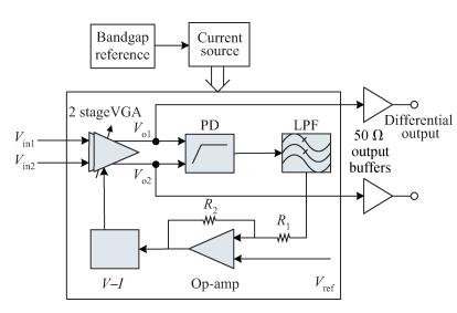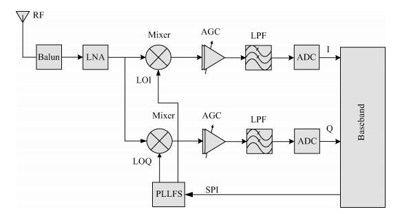
Fig. 1.
The AGC locates in an RFID direct-down receiver architecture.
SEMICONDUCTOR INTEGRATED CIRCUITS
Wenbo Wang1, Luhong Mao1, , Xindong Xiao2, Shilin Zhang1 and Sheng Xie1
Corresponding author: Mao Luhong, Email:lhmao@tju.edu.cn
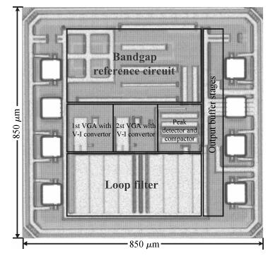
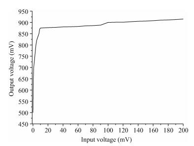
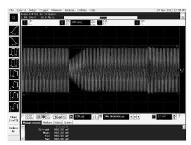
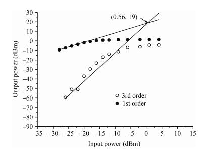
Abstract: A differential automatic gain control (AGC) circuit is presented. The AGC architecture contains two-stage variable gain amplifiers (VGAs) which are implemented with a Gilbert cell, a peak detector (PD), a low pass filter, an operational amplifier, and two voltage to current (V-I) convertors. One stage VGA achieves 30 dB gain due to the use of active load. The AGC circuit is implemented in UMC 0.18-μm single-poly six-metal CMOS process technology. Measurement results show that the final differential output swing of the 2nd stage VGA is about 0.9-Vpp; the total gain of the two VGAs can be varied linearly from-10 to 50 dB when the control voltage varies from 0.3 to 0.9 V. The final circuit (containing output buffers and a band-gap reference) consumes 37 mA from single 1.8 V voltage supply. For a 50 mV amplitude 60% modulation depth input AM signal it needs 100 μs to stabilize the output. The frequency response of the circuit has almost a constant-3 dB bandwidth of 2.2 MHz. Its OIP3 result is at 19 dBm.
Keywords: automatic gain control, variable gain amplifier, exponential V-I convertor, peak detector, gain dynamic range
| [1] |
Zhou M, Fan C, Chen D, et al. A compact automatic gain control loop for GNSS RF receiver. 10th IEEE International Conference on Solid-State and Integrated Circuit Technology (ICSICT), Shanghai, China, 2010:284
|
| [2] |
Calvo B, Sanz M T, Celma S. Low-voltage low-power CMOS programmable gain amplifier. 6th International Caribbean Conference on Devices, Circuits and Systems, Playa del Carmen, Mexico, 2006:101 http://onlinepresent.org/proceedings/vol25_2013/20.pdf
|
| [3] |
Lin Y T, Chen C H, Lu S S. A feed-forward automatic-gain control amplifier for biomedical applications. Asia-Pacific Microwave Conference Proceedings, Bangkok, Thailand, 2007 http://www.nsfc.gov.cn/Portals/0/fj/fj20160106_01.xls
|
| [4] |
Lei Qianqian, Lin Min, Chen Zhiming, et al. A programmable gain amplifier with a DC offset calibration loop for a direct-conversion WLAN transceiver. Journal of Semiconductors, 2011, 32(4):045006 doi: 10.1088/1674-4926/32/4/045006
|
| [5] |
Li Guofeng, Wu Nanjian. A low power flexible PGA for software defined radio systems. Journal of Semiconductors, 2012, 33(5):055006 doi: 10.1088/1674-4926/33/5/055006
|
| [6] |
Wang X, Chi B, Wang Z. A low-power high-data-rate ASK IF receiver with a digital-control AGC loop. IEEE Trans Circuits Syst, 2010, 57(8):617 doi: 10.1109/TCSII.2010.2050954
|
| [7] |
Khoury J M. On the design of constant settling time AGC circuits. IEEE Trans Circuits Syst Ⅱ:Analog and Digital Signal Processing, 1998, 45(3):283 doi: 10.1109/82.664234
|
| [8] |
Jeon O, Fox R M, Myers B A. Analog AGC circuitry for a CMOS WLAN receiver. IEEE J Solid-State Circuits, 2006, 41(10):2291 doi: 10.1109/JSSC.2006.881548
|
| [9] |
Park S B, Wilson J E, Ismail M. The chip-peak detectors for multistandard wireless receivers. IEEE Circuits and Devices Magazine, 2006, 22(6):6 doi: 10.1109/MCD.2006.307270
|
| [10] |
Cheung H Y, Cheung K S, Lau J. A low power monolithic AGC with automatic DC offset cancellation for direct conversion hybrid CDMA transceiver used in telemetering. IEEE International Symposium on Circuits and Systems, Sydney, NSW, Australia, 2001:390 http://cc.ee.nchu.edu.tw/~aiclab/public_htm/Analog/Theses/2000Cheung.pdf
|
| [11] |
Duong Q H, Nguyen T K, Duong H N, et al. dB-linear V-I converter using composite NMOS transistor. Proceedings of the 15th International Conference on Microelectronics, Cairo, Egypt, 2003:409 http://ieeexplore.ieee.org/xpl/articleDetails.jsp?reload=true&arnumber=1287710&filter%3DAND%28p_IS_Number%3A28700%29
|
| [12] |
Ta C M, Yong C H, Yeoh W G. A 2.7 mW, 0.064 mm2 linear-in-dB VGA with 60 dB tuning range, 100 MHz bandwidth, and two DC offset cancellation loops. IEEE International Workshop on Radio-Frequency Integration Technology, Singapore, 2005:74 doi: 10.1007/s11277-016-3186-z
|
| [13] |
Kucharski D, Kornegay K T. Jitter considerations in the design of a 10-Gb/s automatic gain control amplifier. IEEE Trans Microw Theory Tech, 2005, 53(2):590 doi: 10.1109/TMTT.2004.840731
|
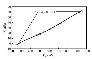
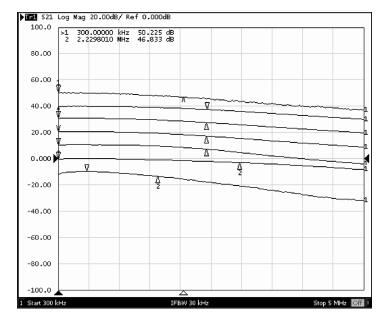
Table 1. Comparison of AGC performance.

|
| [1] |
Zhou M, Fan C, Chen D, et al. A compact automatic gain control loop for GNSS RF receiver. 10th IEEE International Conference on Solid-State and Integrated Circuit Technology (ICSICT), Shanghai, China, 2010:284
|
| [2] |
Calvo B, Sanz M T, Celma S. Low-voltage low-power CMOS programmable gain amplifier. 6th International Caribbean Conference on Devices, Circuits and Systems, Playa del Carmen, Mexico, 2006:101 http://onlinepresent.org/proceedings/vol25_2013/20.pdf
|
| [3] |
Lin Y T, Chen C H, Lu S S. A feed-forward automatic-gain control amplifier for biomedical applications. Asia-Pacific Microwave Conference Proceedings, Bangkok, Thailand, 2007 http://www.nsfc.gov.cn/Portals/0/fj/fj20160106_01.xls
|
| [4] |
Lei Qianqian, Lin Min, Chen Zhiming, et al. A programmable gain amplifier with a DC offset calibration loop for a direct-conversion WLAN transceiver. Journal of Semiconductors, 2011, 32(4):045006 doi: 10.1088/1674-4926/32/4/045006
|
| [5] |
Li Guofeng, Wu Nanjian. A low power flexible PGA for software defined radio systems. Journal of Semiconductors, 2012, 33(5):055006 doi: 10.1088/1674-4926/33/5/055006
|
| [6] |
Wang X, Chi B, Wang Z. A low-power high-data-rate ASK IF receiver with a digital-control AGC loop. IEEE Trans Circuits Syst, 2010, 57(8):617 doi: 10.1109/TCSII.2010.2050954
|
| [7] |
Khoury J M. On the design of constant settling time AGC circuits. IEEE Trans Circuits Syst Ⅱ:Analog and Digital Signal Processing, 1998, 45(3):283 doi: 10.1109/82.664234
|
| [8] |
Jeon O, Fox R M, Myers B A. Analog AGC circuitry for a CMOS WLAN receiver. IEEE J Solid-State Circuits, 2006, 41(10):2291 doi: 10.1109/JSSC.2006.881548
|
| [9] |
Park S B, Wilson J E, Ismail M. The chip-peak detectors for multistandard wireless receivers. IEEE Circuits and Devices Magazine, 2006, 22(6):6 doi: 10.1109/MCD.2006.307270
|
| [10] |
Cheung H Y, Cheung K S, Lau J. A low power monolithic AGC with automatic DC offset cancellation for direct conversion hybrid CDMA transceiver used in telemetering. IEEE International Symposium on Circuits and Systems, Sydney, NSW, Australia, 2001:390 http://cc.ee.nchu.edu.tw/~aiclab/public_htm/Analog/Theses/2000Cheung.pdf
|
| [11] |
Duong Q H, Nguyen T K, Duong H N, et al. dB-linear V-I converter using composite NMOS transistor. Proceedings of the 15th International Conference on Microelectronics, Cairo, Egypt, 2003:409 http://ieeexplore.ieee.org/xpl/articleDetails.jsp?reload=true&arnumber=1287710&filter%3DAND%28p_IS_Number%3A28700%29
|
| [12] |
Ta C M, Yong C H, Yeoh W G. A 2.7 mW, 0.064 mm2 linear-in-dB VGA with 60 dB tuning range, 100 MHz bandwidth, and two DC offset cancellation loops. IEEE International Workshop on Radio-Frequency Integration Technology, Singapore, 2005:74 doi: 10.1007/s11277-016-3186-z
|
| [13] |
Kucharski D, Kornegay K T. Jitter considerations in the design of a 10-Gb/s automatic gain control amplifier. IEEE Trans Microw Theory Tech, 2005, 53(2):590 doi: 10.1109/TMTT.2004.840731
|


Article views: 4820 Times PDF downloads: 90 Times Cited by: 0 Times
Received: 07 May 2012 Revised: 29 August 2012 Online: Published: 01 February 2013
| Citation: |
Wenbo Wang, Luhong Mao, Xindong Xiao, Shilin Zhang, Sheng Xie. A differential automatic gain control circuit with two-stage-10 to 50 dB tuning range VGAs[J]. Journal of Semiconductors, 2013, 34(2): 025008. doi: 10.1088/1674-4926/34/2/025008
****
W B Wang, L H Mao, X D Xiao, S L Zhang, S Xie. A differential automatic gain control circuit with two-stage-10 to 50 dB tuning range VGAs[J]. J. Semicond., 2013, 34(2): 025008. doi: 10.1088/1674-4926/34/2/025008.

|
| [1] |
Zhou M, Fan C, Chen D, et al. A compact automatic gain control loop for GNSS RF receiver. 10th IEEE International Conference on Solid-State and Integrated Circuit Technology (ICSICT), Shanghai, China, 2010:284
|
| [2] |
Calvo B, Sanz M T, Celma S. Low-voltage low-power CMOS programmable gain amplifier. 6th International Caribbean Conference on Devices, Circuits and Systems, Playa del Carmen, Mexico, 2006:101 http://onlinepresent.org/proceedings/vol25_2013/20.pdf
|
| [3] |
Lin Y T, Chen C H, Lu S S. A feed-forward automatic-gain control amplifier for biomedical applications. Asia-Pacific Microwave Conference Proceedings, Bangkok, Thailand, 2007 http://www.nsfc.gov.cn/Portals/0/fj/fj20160106_01.xls
|
| [4] |
Lei Qianqian, Lin Min, Chen Zhiming, et al. A programmable gain amplifier with a DC offset calibration loop for a direct-conversion WLAN transceiver. Journal of Semiconductors, 2011, 32(4):045006 doi: 10.1088/1674-4926/32/4/045006
|
| [5] |
Li Guofeng, Wu Nanjian. A low power flexible PGA for software defined radio systems. Journal of Semiconductors, 2012, 33(5):055006 doi: 10.1088/1674-4926/33/5/055006
|
| [6] |
Wang X, Chi B, Wang Z. A low-power high-data-rate ASK IF receiver with a digital-control AGC loop. IEEE Trans Circuits Syst, 2010, 57(8):617 doi: 10.1109/TCSII.2010.2050954
|
| [7] |
Khoury J M. On the design of constant settling time AGC circuits. IEEE Trans Circuits Syst Ⅱ:Analog and Digital Signal Processing, 1998, 45(3):283 doi: 10.1109/82.664234
|
| [8] |
Jeon O, Fox R M, Myers B A. Analog AGC circuitry for a CMOS WLAN receiver. IEEE J Solid-State Circuits, 2006, 41(10):2291 doi: 10.1109/JSSC.2006.881548
|
| [9] |
Park S B, Wilson J E, Ismail M. The chip-peak detectors for multistandard wireless receivers. IEEE Circuits and Devices Magazine, 2006, 22(6):6 doi: 10.1109/MCD.2006.307270
|
| [10] |
Cheung H Y, Cheung K S, Lau J. A low power monolithic AGC with automatic DC offset cancellation for direct conversion hybrid CDMA transceiver used in telemetering. IEEE International Symposium on Circuits and Systems, Sydney, NSW, Australia, 2001:390 http://cc.ee.nchu.edu.tw/~aiclab/public_htm/Analog/Theses/2000Cheung.pdf
|
| [11] |
Duong Q H, Nguyen T K, Duong H N, et al. dB-linear V-I converter using composite NMOS transistor. Proceedings of the 15th International Conference on Microelectronics, Cairo, Egypt, 2003:409 http://ieeexplore.ieee.org/xpl/articleDetails.jsp?reload=true&arnumber=1287710&filter%3DAND%28p_IS_Number%3A28700%29
|
| [12] |
Ta C M, Yong C H, Yeoh W G. A 2.7 mW, 0.064 mm2 linear-in-dB VGA with 60 dB tuning range, 100 MHz bandwidth, and two DC offset cancellation loops. IEEE International Workshop on Radio-Frequency Integration Technology, Singapore, 2005:74 doi: 10.1007/s11277-016-3186-z
|
| [13] |
Kucharski D, Kornegay K T. Jitter considerations in the design of a 10-Gb/s automatic gain control amplifier. IEEE Trans Microw Theory Tech, 2005, 53(2):590 doi: 10.1109/TMTT.2004.840731
|

 WeChat ID
Journal of Semiconductors © 2017 All Rights Reserved 京ICP备05085259号-2

 DownLoad: