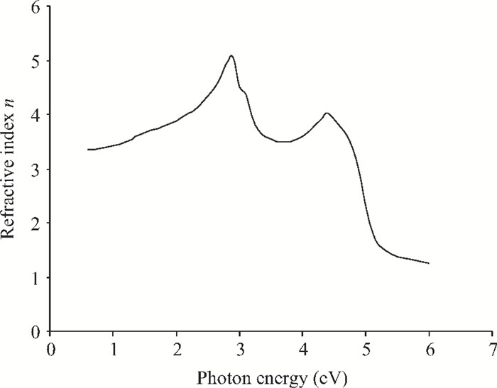
Loading [MathJax]/jax/output/HTML-CSS/jax.js
J. Semicond. > 2013, Volume 34 > Issue 3 > 032002

SEMICONDUCTOR PHYSICS

Optical properties of GaAs

J.O. Akinlami and A.O. Ashamu

+ Author Affiliations

 Corresponding author: J. O. Akinlami, Email:johnsonak2000@yahoo.co.uk

DOI: 10.1088/1674-4926/34/3/032002

PDF

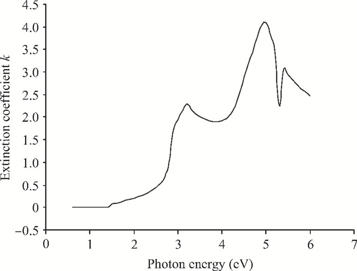
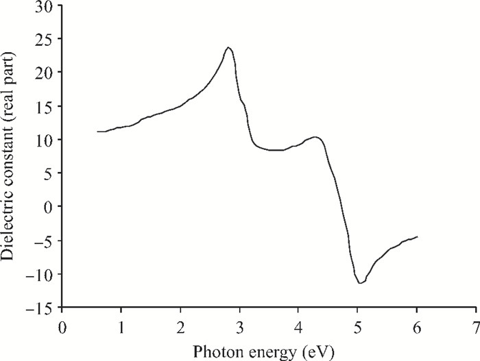
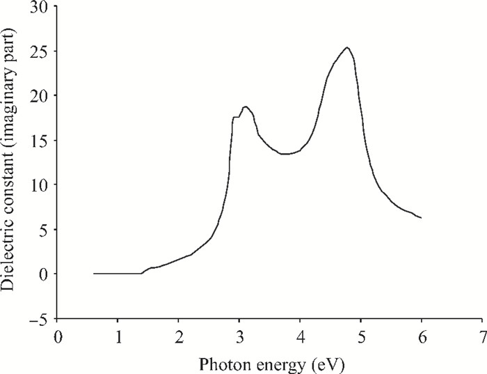
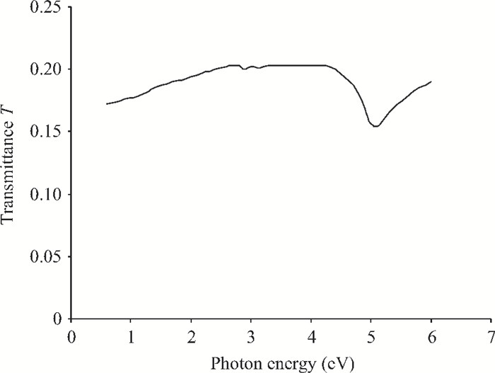
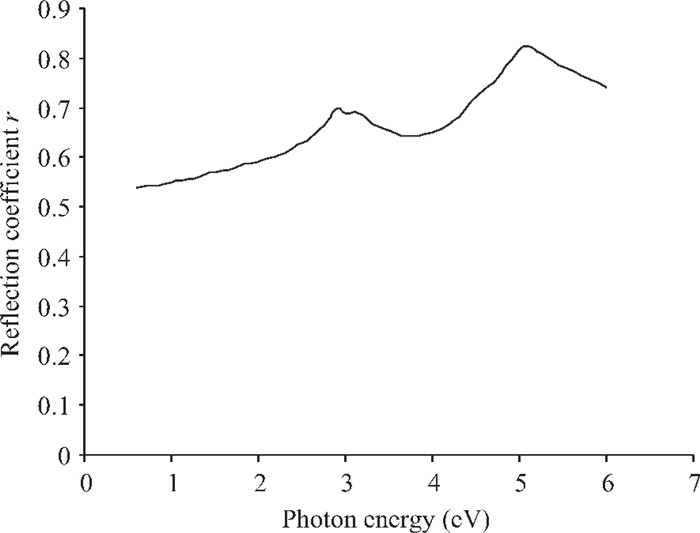
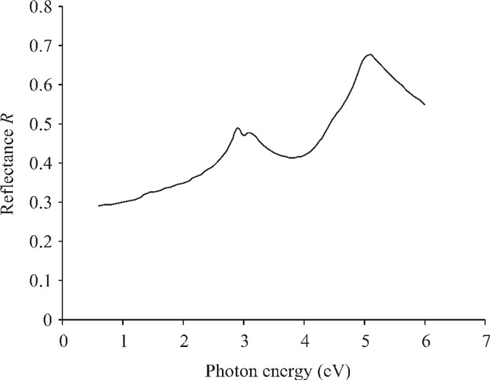
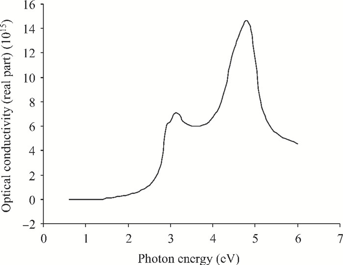
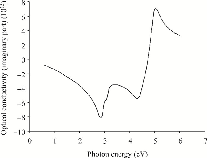
Abstract: We have investigated the optical properties of gallium arsenide (GaAs) in the photon energy range 0.6-6.0 eV. We obtained a refractive index which has a maximum value of 5.0 at a photon energy of 3.1 eV; an extinction coefficient which has a maximum value of 4.2 at a photon energy of 5.0 eV; the dielectric constant, the real part of the complex dielectric constant has a maximum value of 24 at a photon energy of 2.8 eV and the imaginary part of the complex dielectric constant has a maximum value of 26.0 at a photon energy of 4.8 eV; the transmittance which has a maximum value of 0.22 at a photon energy of 4.0 eV; the absorption coefficient which has a maximum value of 0.22×10⁸ m-1 at a photon energy of 4.8 eV, the reflectance which has a maximum value of 0.68 at 5.2eV; the reflection coefficient which has a maximum value of 0.82 at a photon energy of 5.2 eV; the real part of optical conductivity has a maximum value of 14.2×10¹⁵ at 4.8 eV and the imaginary part of the optical conductivity has a maximum value of 6.8×10¹⁵ at 5.0 eV. The values obtained for the optical properties of GaAs are in good agreement with other results.

Key words: complex index of refractionextinction coefficientcomplex dielectric constanttransmittanceabsorption coefficientsemiconductor and photon energy

Accurate device modeling is essential for circuit simulation and design. In 1996, BSIM3 Version 3 (commonly abbreviated as BSIM3v3) was established by SEMATECH as the first industry-wide standard of its kind[1]. It has since been widely used by most semiconductor and IC design companies world-wide for device modeling and CMOS IC design. Though the BSIM model is accurate, it needs a long time to adjust for non-ideal effects. Meanwhile, Moore’s law has nearly come to an end and lots of new devices show up which need study[24]. It is unwise to invest a huge amount of resources to model a new device; we may just test its circuit characteristics rather than business use. Efficient modeling methods should be proposed for these purposes.

A lot of methods have been proposed for the similar usage. Gustanven proposed a lot of black box Macro-modeling methods for huge complex systems such as the high-voltage system and electronic magnetic system[5]. The whole large systems are viewed as a black box with input and output, and statistical regression models are built to describe these systems. By using this method, the complexity of systems is greatly reduced[68]. The same thought can be used in semiconductor device modeling since a semiconductor device can also be viewed as a black box. If an ideal statistical regression model is found, we can save a lot of time and money. For example, the carbon nanotubes field effect transistor (CNT-FET) is a promising candidate for MOS-FET, which generates much less heat and runs as fast as MOS-FET[9]. But CNT-FET shows different I–V characteristics with a different manufacturing process, which is hard for us to build a universal physical model for all of them. A black box statistical modeling is a choice for efficiently modeling different CNT-FET[10, 11].

The keys of statistical modeling are the choice of model and at what extent the model can fit the true data to. Numerous statistical models are proposed for this task. Ordinary least square (OLS) and its regularization method (Ridge and LASSO) are the most commonly used regression approaches[12]. But they are mainly used for linear regression and may not fit for semiconductor device modeling, since the device has a highly nonlinear property. In this paper, we propose two numerical methods for semiconductor device modeling, single-pole denominator numerator fitting (single-pole MRR) and double-pole MRR. They have a great nonlinear curve fitting ability and good numerical stability which are critical in semiconductor device modeling.

A lot of methods have been proposed for the curve fitting task. Suppose we have p dimension input attributes and one dimension output observed data points from the curve, (xi,yi),i=1,...,K,xiRP,yiR,PN+. We want to find a model ˆyi=g(xi) to best fit our original curve. OLS (Ordinary Least Square) has been widely used as a linear regression method, which supposes the input and output has a simple linear relationship. Firstly, using system input attributes x to construct a feature vector X , then, combining these features linearly to get one output ˆy=g(x;w)=XTw,wRP . OLS tries to minimize the least square error of true data and model output to find optimal parameters, this is also called objective function,

w=argminw||yXTw||2. (1)

If XTX is invertible, the optimal solution of coefficient w is w* = (XTX)–1XTy[1]. The Lasso is a shrinkage method for OLS, which adds the L1 norm to the objective function,

w=argminw||yXTw||2+λPj=1wj. (2)

It can shrink some of the parameters to be exactly zeros if positive penalty λ is large enough to achieve higher predict accuracy and interpretation[1]. Though a basis function such as polynomial basis and triangle basis can be used for nonlinear expansion, the OLS and Lasso suffer from its linear nature and behave not so well on a nonlinear curve fitting task.

Compared with the linear models, the rational model, y=N(x)/D(x)=XTwn/XTwd , has nonlinearity in nature, thus is more suitable for fitting a nonlinear curve. The optimal rational model for a system can be obtained through minimizing objective function,

w=argminw||yN(X)D(X)||2. (3)

However, Eq. (3) cannot be solved directly in closed form as there are unknown parameters in the denominator.

Since the 1950s, considerable effort has been devoted to the development of methods for parameters extraction of rational function. Levy, Sanathanan and Koerner, Lawrence and Rogers, and Stahl have presented various techniques by posing linear least squares problems. Pintelon and Guilaume analyze these and several other techniques[1316]. Vector-Fitting(VF), introduced by Gustavsen and Semlyen and using partial fraction basis, has been widely accepted as a robust modeling method for approximating frequency domain responses[1719].

In this work, we proposed single-pole MRR and double-pole MRR methods based on vector fitting, which are of great help in a nonlinear curve fitting task. The power of MRR is shown by numerical examples involving artificially created binary function, SMIC 40 nm NMOS DC characteristic, CNT-FET, and the LNA performance model.

Consider the rational function approximation,

y=N(X)D(X)=w0+XTwn1XTwd, (4)

where X is a feature vector formed by input attributes x (x is a column vector and its elements are input variable, like x1,x2,x3 and so on). We can use a different basis function to map input attributes x to feature vector X . For example, X=[x1,x2,x3,x21,x22,x23,...]T .

We solve Eq. (4) by transforming it into an iterating OLS problem. We knew that equation y=XTw can be solved by objective function equation 1. In rational function approximation Eq. (4), we have object function,

wn,wd=argminwn,wd||yw0+XTwn1XTwd||2. (5)

Suppose in our iteration process, we have a set of {wtd},t=0,1,...w0d=0 and wt1d is known in the ith iteration, where t is the iteration step of the whole process. We multiply a factor ||1XTwtd1XTwt1d||2 to Eq. (5), and let wtd=wt1d+w+d ,

||1XTwtd1XTwt1d||2argminwn,wd||yw0+XTwtn1XTwtd||2=argmin||wn,wd(1XTw+d1XTwt1d)(yw0+XTwtn1XTwtd)||2=argminwn,wd||yXTw+dy1XTwt1dw0+XTwtn1XTwt1d||2=argminwn,wd||yw0+XTwtn+XTyw+d1XTwt1d||2. (6)

Here in the last equation, a new OLS problem is made where the feature vector is [11XTwt1d,XT1XTwt1d,XTy1XTwt1d] and coefficient is [w0,wtn,w+d] . By solving this OLS problem we get w+d and wtd can be solved by wtd=wt1d+w+d . In the (t+1)th iteration, wtd is known, and we continue the above iteration until the convergence of wd . If limtwtd=C , we will have limtw+d=wtdwt1d=0 and the factor will be limt||1XTwtd1XTwt1d||2=1 . We will get the optimal solution wn,wd if wd converges.

Consider the rational function approximation,

y=N(X)D(X)=w01+XTwn11XTwd1+w02+XTwn21XTwd2. (7)

Though we can still multiply a factor ||1XTwtd11XTwt1d1 1XTwtd21XTwt1d2||2 to its objective function, the equation may have too many matrix products such as XTwd1XTwd2 and is hard to solve. The same as single-pole MRR, we transform Eq. (7) by adding two additional elements in the tth iteration,

wt01+XTwtn11XTwt1d1+wt02+XTwtn21XTwt1d2=(1XTw+d11XTwt1d1XTw+d21XTwt1d2)y, (8)
wt01+XTwtn11XTwt1d1+wt02+XTwtn21XTwt1d2+XTyw+d11XTwt1d1+XTyw+d21XTwt1d2=y. (9)

Here wt1d1+w+d1=wtd1 , wt1d2+w+d2=wtd2 . A new OLS problem is made where the feature vector is [11XTwt1d1, XT1XTwt1d1,11XTwt1d2,XT1XTwt1d2,XTy1XTwt1d1,XTy1XTwt1d2] and the coefficient is [wt01,wtn1,wt02,wtn2,w+d1,w+d2] . We continue the above iteration until the convergence of wd1,wd2 . Different from the single-pole MRR, if we set wd1,wd2 to zero as the initial value, the equation will suffer from rank deficiency, the solution is we get the value of wd1,wd2 from a random normal distribution with zero mean and small variance. In fact, if we get the initial value of wd from a random normal distribution rather than zero in single-pole MRR, the convergence value of wd will not change. This means the random initial value of wd will not affect the final convergence, and the same goes for double-pole MRR.

The key step of MRR is accurately solving the over-determined Eq. (7). However, because the condition of such a problem is poor, the solving of the normal equation is of reduced numerical stability and may result in large errors in the solution. Besides, if there are degrees of magnitude difference between y and x, the rank of matrix A might be rank deficient, which also lead to the worst solution. In order to circumvent these cases, normalizing input attributes x and target output y before the parameters extraction procedure is usually of great help.

Semiconductor device I–V characteristic value might be small in number and varies in a wide range, e.g. the Idof NMOS-FET may vary from 1×10⁵to1×1013 . Log transformation is important in this circumstance. However, this will also require high precision of the model since inverse operation, exponentiation, will zoom in the prediction error dramatically.

To illustrate the validity of the proposed method, we firstly consider an artificially created function defined y=sin(2x21+x22)/(2x21+x22),x1,x2[3,3] . We adopt Single-pole MRR with the decic polynomial basis. Figs. 1(a) and 1(b) show the origin function and MRR fitting result. The normalized mean-squared-error (NMSE) is about 7.45 × 10⁻¹⁰. Figs. 1(c) and 1(d) show the step NMSEs of two MRR methods, and that single-pole MRR achieves better accuracy and stability. So in this fitting task, we adopt single-pole MRR as fitting model.

Figure  1.  (Color online) The original function and MRR fitting function. (a) Original artificial function. (b) Single-pole MRR fitting result. (c) Step NMSEs of single-pole MRR. (d) Step NMSEs of double-pole MRR.

DC characteristics of NMOS-FET are used to show the performance of MRR, compared with OLS and LASSO. As BSIM has been widely used in industry for years and, to some extent, it can represent the authentic physical property of NMOS-FET, so we use Cadence and SPICE to get DC simulation data of SMIC 40 nm NMOS-FET with a channel width of 1 μm and channel length of 40 nm. In this case, we choose two independent variables, Vd and Vg , and one dependent variable, Id .

Fig. 2 shows the fitting results of different algorithms for the dataset. We plot the IdVd curve and IdVg curves to show the fitting performance. Table 1 shows the parameters and NMSE of the fitting result. Single-pole MRR with sextic polynomial, double-pole MRR with quartic polynomial and OLS nonic polynomial are used for contrast. The number of parameters in each model is close. Because of the regularization property, we choose the nonic polynomial for LASSO to include as many meaningful features as possible. After 10-fold cross validation, the optimal regularization parameter λ in Eq. (2) is 1 and the number of non-zero coefficient is 36. Normalization and logarithm transformation are both used as preprocessing methods. Two MRR algorithms outperform OLS and LASSO, as shown in Fig. 2. For convenience, we zoom-in the IdVg curve and clip two ranges of Vg from each curve. The detail of the fitting result can then be seen clearly in Fig. 3.

Table  1.  NMSE and parameters number results of different algorithms.
Algorithm Single-pole MRR
(sextic polynomial)
Double-pole MRR
(quartic polynomial)
OLS
(nonic polynomial)
LASSO
(nonic polynomial)
Parameter 55 58 55 36
NMSE 3.0157 × 10⁻⁸ 2.631 × 10⁻⁶ 4.357 × 10⁻⁴ 5.082 × 10⁻⁴
DownLoad: CSV  | Show Table
Figure  2.  (Color online) The fitting results of different algorithms. (a) IdVd curve by single-pole MRR. (b) IdVg curve by single-pole MRR. (c) IdVd curve by double-pole MRR. (d) IdVg curve by double-pole MRR. (e) IdVd curve by OLS. (f) IdVg curve by OLS. (g) IdVd curve by LASSO. (h) IdVg curve by LASSO.
Figure  3.  (Color online) Zoom-in pictures of IdVg curves fitting by different algorithms. (a) Zoom-in of IdVg curve by single-pole MRR, Vg ranges from 0.15 to 0.45 V. (b) Zoom-in of IdVg curve by single-pole MRR, Vg ranges from 0.65 to 1.1 V. (c) Zoom-in of IdVg curve by double-pole MRR, Vg ranges from 0.15 to 0.45 V. (d) Zoom-in of IdVg curve by double-pole MRR, Vg ranges from 0.65 to 1.1 V. (e) Zoom-in of IdVg curve by OLS, Vg ranges from 0.15 to 0.45 V. (f) Zoom-in of IdVg curve by single-pole MRR, Vg ranges from 0.65 to 1.1 V. (g) Zoom-in of IdVg curve by LASSO, Vg ranges from 0.15 to 0.45 V. (h) Zoom-in of IdVg curve by LASSO, Vg ranges from 0.65 to 1.1 V.

The Table 1 details the NMSE of four algorithms. As the data is very small, the Normalized Mean Square Error (NMSE) is used, as shown in Eq. 10. Single-pole MRR with sextic polynomial

1mKi=1[timax(t)yimax(t)]2. (10)

NMSE is 3.0157×10⁸ and double-pole MRR with cubic polynomial’s NMSE is 2.631×10⁶ . The result shows MRRs have a much better nonlinear curve fitting ability than OLS and LASSO. We also compare the computation complexity with OLS and LASSO in this paper. Double-pole MRR reach smaller NMSE than OLS and LASSO with less parameters. It is more efficient than the classics. The time complexity of MRR is iteration time plus the time period of a single iteration of MRR. The time of a single iteration of MRR is equal to other classics. The MRR will converge in less than 10 iterations. This will be discussed in Section 4.2.2. In all of the experiments in this paper, the iteration time is no longer than 1 s. The experiment environment is Intel i7-4790 CPU with 32G memory and MATLAB 2017b.

Although single-pole MRR reaches the minimum of NMSE in the results, double-pole MRR uses a lower polynomial (cubic polynomial) and the fewest parameters to reach the second best fitting solution. In fact, it is the best model with polynomial of low degree (1, 2, 3). Double-pole MRR with cubic polynomial’s NMSE is 1.593 × 10⁻⁵. This is very helpful in the circumstance where the number of input attributes is large and polynomial of a high degree cannot be achieved due to the limit of CPU memory, e.g. a sextic polynomial of 12 input attributes requires 1237 GB CPU memory.

The convergence of the algorithm is critical, for our parameters extraction method is based on iteration. As has been analyzed, the stability of every least squared problem would be improved after data normalization. Single-pole MRR has very good numerical stability with all polynomial while double-pole MRR shows good numerical stability for a polynomial of low degrees. When the polynomial degree is high, double-pole MRR may suffer from rank deficiency and the numerical stability will decrease. We get the sequential NMSE of two MRRs’ iteration with a quadratic polynomial. The result is plotted in Fig. 4 in log scale. Fig. 4(a) shows step NMSEs of the global optimal fitting results for 40 nm MOSFET. Single-pole MRR adopts a sextic polynomial and double-pole MRR adopts a quartic polynomial. Fig. 4(b) shows step NMSEs of two MRR methods when they adopt the quadratic polynomial. The best NMSE of single-pole MRR and double-pole MRR with the quadratic polynomial are 5.94×10² and 2.851×10⁵ .

In this section, we apply single-pole MRR to CNT-FET DC behavior modeling. Fig. 4 visualizes the measured Id with respect to Vd and Vg for a CNT-FET ( w=3μm and l=15nm ). Vg ranges from −2 to 0 V with a step size 0.15 V and Vd ranges from −2 to 0.02 V with a step size 0.02 V. We choose a septic polynomial to generate feature vector X.

Figure  4.  (Color online) Step NMSEs of two MRR methods in different polynomial degrees. (a) Step NMSEs of MRR methods in the situation of a polynomial of high degree. (b) Step NMSEs of MRR methods in the situation of a polynomial of low degree.

Normalized mean square error (NMSE) of Idis 5.961×10⁴ . Fig. 5 shows the original data surface and fitting data surface generated by single-pole MRR. Figs. 6(a)6(d) shows the fitting result of output characteristics (|Id|–|Vd|) and transfer characteristics (|Id|–|Vg|) respectively. The prediction fits the measured data well. Figs. 6(e) and 6(f) show the step NMSEs of two MRR methods, they all can converge but the single-pole MRR outperforms the double-pole MRR in the global optimal NMSE, so we choose single-pole MRR as our final fitting model. Considering the manufacturing process of CNT-FET is not mature, there is still great uncertainty in devices, so we think this fitting result is acceptable.

Figure  5.  (Color online) The observed CNT-FET data point surface and MRR fitting surface. (a) Original data of CNT-FET. (b) Single-pole MRR fitting result.
Figure  6.  (Color online) |Id|–|Vd|, |Id|–|Vg| curves and step NMSEs by MRR methods. (a) |Id|–|Vd| curve by single-pole MRR. (b) |Id|–|Vg| curve by single-pole MRR. (c) Zoom-in |Id|–|Vg| curve, Vg ranges from 0–0.8 V. (d) Zoom-in |Id|–|Vg| curve, Vg ranges from 1–2 V. (e) Step NMSEs of single-pole MRR. (f) Step NMSEs of double-pole MRR.

In this section we apply MRR methods to model LNA performance characteristics and demonstrate our algorithm in multi-variables (more than 2) regression. Generally, we get a certain performance of a circuit by means of solving the KCL and KVL equations. The solution is accurate but very time-consuming. If we want to do behavioral simulation and optimization for the RF circuit, directly mathematical mapping between design parameters and performance is highly useful.

We chose an LNA which worked at 4GHz and use Cadence to get simulation data for modeling. Figs. 7(a)7(c) show the fitting result of three LNA indicators, NF (noise factor), gain and power by single-pole MRR. Figs. 7(d)7(f) are step NMSEs of single-pole MRR and Figs. 7(g)7(i) are step NMSEs of double-pole MRR. The performance of two MRR methods are close. We sort the sample point in an increased order and record the index sequence, then we plot data points, predictions and errors according to the sorted index sequence in one figure. We can see that the training result is good. Normalized mean square error (NMSE) of NF, gain and power are 0.0031, 0.00710, and 3.5887×10⁷ .

Figure  7.  (Color online) The original function and MRR fitting function. (a) Noise factor fitting by single-pole MRR. (b) Gain fitting by single-pole MRR. (c) Power fitting by single-pole MRR.(d) Step NMSEs of single-pole MRR for noise factor. (e) Step NMSEs of single-pole MRR for gain. (f) Step NMSEs of single-pole MRR for power. (g) Step NMSEs of double-pole MRR for noise factor. (h) Step NMSEs of double-pole MRR for gain. (i) Step NMSEs of double-pole MRR for power.

This paper proposes a family of numerical methods---MRR to approximate an unknown system and extract model parameters. We firstly use single-pole MRR to fit an artificial function and the result is extremely good. Then we compare the performance among single-pole MRR, double-pole MRR, OLS and LASSO on SMIC 40 nm DC characteristics dataset. The results show single-pole MRR has the highest fitting precision and double-pole performs better than single-pole MRR in circumstances of a low degree polynomial. The MRR methods have a more powerful nonlinear curve fitting ability than OLS and LASSO and are proved to be numerically stable. CNT-FET and LNA performance indicators are also modeled, of which the fitting results are good as well. But there are two key points for using MRR methods. Firstly, users have to pay close attention to the numerical stability of MRR methods. We have done one artificial function fitting task and three device model fitting tasks for the convergence analysis of two MRR methods. The results show single-pole MRR has better numerical stability than double-pole MRR. Secondly, the datasets used for the fitting curve should be well-distributed and not be sparse. MRR methods are powerful in fitting a highly-nonlinear function but can also lead to overfitting if the dataset is ill-distributed. Our paper shows the MRR methods are good choices for semiconductor devices statistical modeling as well as other highly-nonlinear curve fitting tasks.


[1]
Sze S M. Physics of semiconductor devices. New York:Wiley, 1969 http://adsabs.harvard.edu/abs/1981psd..book.....S
[2]
Beliles R P. The metals. In:Clayton G D, Clayton F E, ed. Patty's industrial hygiene and toxicology. Vol. 26. 4th ed. New York:John Wiley and Sons, 1994:1879 http://www.cqvip.com/QK/94689X/201303/45044662.html
[3]
Sabot J L, Lauvray H. Gallium and gallium compounds. In:Kroschwitz J I, Howe-Grant M, ed. Kirk-Othmer encyclopedia of chemical technology. 4th ed. Vol. 12. New York:John Wiley and Sons, 1994:299
[4]
Goldschmidt V M. Crystal structure and chemical constitution. Trans Faraday Soc, 1929, 25:253 doi: 10.1039/tf9292500253
[5]
Tibermacine T, Mercizga A. Revue des energies renouvelables, 2009, 12(1):125
[6]
Sze S M, Ng K K. Physics of semiconductor devices. 3rd ed. John Wiley and Sons, Inc., 2007
[7]
Jovanovic D, Gajic R, Hingerl K. Optical properties of GaAs 2D Archimedean photonic lattice tiling with the p4g symmetry. Science of Sintering, 2008, 40:167 doi: 10.2298/SOS0802167J
[8]
Ghosh C, Pal S, Goswami B, et al. Theoretical study of the electronic structure of GaAs nanotubes. J Phys Chem C, 2007, 111:12284 doi: 10.1021/jp0746695
[9]
Ng K K. Complete guide to semiconductor device. 2nd ed. New York:Wiley, 2002
[10]
Colombo C, Hei M, Gratzel M, et al. Gallium arsenide P-I-N radial structures for photovoltaic applications. Appl Phys Lett, 2009, 94:173108 doi: 10.1063/1.3125435
[11]
Kendall E J M. Transistors. New York:Pergamon Press, 1969
[12]
Wallmark J T. Field-effect transistors, physics, technology and applications. Prentice-Hall, Englewood Cliff, 1966
[13]
Liou J J, Schwierz F. RF MOSFET:recent advances, current status and future trends. Solid-State Electron, 2003, 47:1881 doi: 10.1016/S0038-1101(03)00225-9
[14]
Chakrabarti N B. GaAs integrated circuits. J Inst Electron Telecommun Eng, 1992, 38:163
[15]
Greber J F. Gallium and gallium compounds. In:Ullmann's encyclopedia of industrial chemistry. 6th Rev. ed. Vol. 15. Weinheim, Wiley-VCH Verlag GmbH and CO., 2003:235 http://www.cqvip.com/QK/94689X/201303/45044662.html
[16]
Fox M. Optical properties of solids. Oxford University Press, 2001:3 doi: 10.1119/1.1987434
[17]
Yu P Y, Cardona M. Fundamentals of semiconductors. Berlin:Springer-Verlag, 1996
[18]
Schubert E F. Refractive index and extinction coefficient of materials. 2004. http://www.rpi.edu/~schubert/Educational-resources/Materials-Refractive-index-and-extinction-coefficient.pdf
[19]
Goswami A. Thin film fundamentals. New Delhi:New Age International, 2005 https://www.ncbi.nlm.nih.gov/pubmed/21928861
[20]
Sharma P, Katyal S C. Determination of optical parameters of a-(As2Se3)90Ge10 thin film. J Phys D:Appl Phys, 2007, 40:2115 doi: 10.1088/0022-3727/40/7/038
[21]
Blakemore J S. Semiconducting and other major properties of gallium arsenide. J Appl Phys, 1982, 53:10 doi: 10.1063/1.331665
[22]
Brian R B, Richard A S, Jesus A D. Carrier-induced change in refractive index of InP, GaAs and InGaAsP. IEEE J Quantum Electron, 1990, 26(1):113 doi: 10.1109/3.44924
[23]
De Boeij P L, Wijers C M J. Ab initio calculations of the reflectance anisotropy of GaAs (110):the role of nonlocal polarizability and local fields. Phys Lett A, 2000, 272:264 doi: 10.1016/S0375-9601(00)00427-8
[24]
Lautenschlager P, Garriga M, Logothetidis M. Interband critical points of GaAs and their temperature dependence. Cardona Phys Rev B, 1987, 35:9174 doi: 10.1103/PhysRevB.35.9174
[25]
Alouani M, Brey L, Christensen N E. Calculated optical properties of semiconductors. Phys Rev B, 1988, 37(3):1167 doi: 10.1103/PhysRevB.37.1167
[26]
Sturge M D. Optical absorption of gallium arsenide between 0.6 and 2.75 eV. Phys Rev, 1962, 127(3):768 doi: 10.1103/PhysRev.127.768
[27]
Aloulou S, Fathallah M, Oueslati M, et al. Determination of absorption coefficients and thermal diffusivity of modulated doped GaAlAs/GaAs heterostructure by photothermal deflection spectroscopy. American Journal of Applied Sciences, 2005, 2(10):1412 doi: 10.3844/ajassp.2005.1412.1417
[28]
Holm R T, Gibson J W, Palik E D. Infrared reflectance studies of bulk and epitaxial-film n-type GaAs. J Appl Phys, 1977, 48:212 doi: 10.1063/1.323322
[29]
El-Nahass M M, Youssef S B, Ali H A M. Optical properties of Zn doped GaAs single crystals. J Optoelectron Adv Mater, 2011, 13(1):76
[30]
Phillip H R, Ehrenreich H. optical properties of semiconductors. Phys Rev, 1963, 129:1550 doi: 10.1103/PhysRev.129.1550
Fig. 1.  Refractive index of GaAs.

Fig. 2.  Extinction coefficient of GaAs.

Fig. 3.  Complex dielectric constant (real part) of GaAs.

Fig. 4.  Complex dielectric constant (imaginary part) of GaAs.

Fig. 5.  Transmittance of GaAs.

Fig. 6.  Absorption coefficient of GaAs.

Fig. 7.  Reflection coefficient of GaAs.

Fig. 8.  Reflectance of GaAs.

Fig. 9.  Optical conductivity (real part) of GaAs.

Fig. 10.  Optical conductivity (imaginary part) of GaAs.

[1]
Sze S M. Physics of semiconductor devices. New York:Wiley, 1969 http://adsabs.harvard.edu/abs/1981psd..book.....S
[2]
Beliles R P. The metals. In:Clayton G D, Clayton F E, ed. Patty's industrial hygiene and toxicology. Vol. 26. 4th ed. New York:John Wiley and Sons, 1994:1879 http://www.cqvip.com/QK/94689X/201303/45044662.html
[3]
Sabot J L, Lauvray H. Gallium and gallium compounds. In:Kroschwitz J I, Howe-Grant M, ed. Kirk-Othmer encyclopedia of chemical technology. 4th ed. Vol. 12. New York:John Wiley and Sons, 1994:299
[4]
Goldschmidt V M. Crystal structure and chemical constitution. Trans Faraday Soc, 1929, 25:253 doi: 10.1039/tf9292500253
[5]
Tibermacine T, Mercizga A. Revue des energies renouvelables, 2009, 12(1):125
[6]
Sze S M, Ng K K. Physics of semiconductor devices. 3rd ed. John Wiley and Sons, Inc., 2007
[7]
Jovanovic D, Gajic R, Hingerl K. Optical properties of GaAs 2D Archimedean photonic lattice tiling with the p4g symmetry. Science of Sintering, 2008, 40:167 doi: 10.2298/SOS0802167J
[8]
Ghosh C, Pal S, Goswami B, et al. Theoretical study of the electronic structure of GaAs nanotubes. J Phys Chem C, 2007, 111:12284 doi: 10.1021/jp0746695
[9]
Ng K K. Complete guide to semiconductor device. 2nd ed. New York:Wiley, 2002
[10]
Colombo C, Hei M, Gratzel M, et al. Gallium arsenide P-I-N radial structures for photovoltaic applications. Appl Phys Lett, 2009, 94:173108 doi: 10.1063/1.3125435
[11]
Kendall E J M. Transistors. New York:Pergamon Press, 1969
[12]
Wallmark J T. Field-effect transistors, physics, technology and applications. Prentice-Hall, Englewood Cliff, 1966
[13]
Liou J J, Schwierz F. RF MOSFET:recent advances, current status and future trends. Solid-State Electron, 2003, 47:1881 doi: 10.1016/S0038-1101(03)00225-9
[14]
Chakrabarti N B. GaAs integrated circuits. J Inst Electron Telecommun Eng, 1992, 38:163
[15]
Greber J F. Gallium and gallium compounds. In:Ullmann's encyclopedia of industrial chemistry. 6th Rev. ed. Vol. 15. Weinheim, Wiley-VCH Verlag GmbH and CO., 2003:235 http://www.cqvip.com/QK/94689X/201303/45044662.html
[16]
Fox M. Optical properties of solids. Oxford University Press, 2001:3 doi: 10.1119/1.1987434
[17]
Yu P Y, Cardona M. Fundamentals of semiconductors. Berlin:Springer-Verlag, 1996
[18]
Schubert E F. Refractive index and extinction coefficient of materials. 2004. http://www.rpi.edu/~schubert/Educational-resources/Materials-Refractive-index-and-extinction-coefficient.pdf
[19]
Goswami A. Thin film fundamentals. New Delhi:New Age International, 2005 https://www.ncbi.nlm.nih.gov/pubmed/21928861
[20]
Sharma P, Katyal S C. Determination of optical parameters of a-(As2Se3)90Ge10 thin film. J Phys D:Appl Phys, 2007, 40:2115 doi: 10.1088/0022-3727/40/7/038
[21]
Blakemore J S. Semiconducting and other major properties of gallium arsenide. J Appl Phys, 1982, 53:10 doi: 10.1063/1.331665
[22]
Brian R B, Richard A S, Jesus A D. Carrier-induced change in refractive index of InP, GaAs and InGaAsP. IEEE J Quantum Electron, 1990, 26(1):113 doi: 10.1109/3.44924
[23]
De Boeij P L, Wijers C M J. Ab initio calculations of the reflectance anisotropy of GaAs (110):the role of nonlocal polarizability and local fields. Phys Lett A, 2000, 272:264 doi: 10.1016/S0375-9601(00)00427-8
[24]
Lautenschlager P, Garriga M, Logothetidis M. Interband critical points of GaAs and their temperature dependence. Cardona Phys Rev B, 1987, 35:9174 doi: 10.1103/PhysRevB.35.9174
[25]
Alouani M, Brey L, Christensen N E. Calculated optical properties of semiconductors. Phys Rev B, 1988, 37(3):1167 doi: 10.1103/PhysRevB.37.1167
[26]
Sturge M D. Optical absorption of gallium arsenide between 0.6 and 2.75 eV. Phys Rev, 1962, 127(3):768 doi: 10.1103/PhysRev.127.768
[27]
Aloulou S, Fathallah M, Oueslati M, et al. Determination of absorption coefficients and thermal diffusivity of modulated doped GaAlAs/GaAs heterostructure by photothermal deflection spectroscopy. American Journal of Applied Sciences, 2005, 2(10):1412 doi: 10.3844/ajassp.2005.1412.1417
[28]
Holm R T, Gibson J W, Palik E D. Infrared reflectance studies of bulk and epitaxial-film n-type GaAs. J Appl Phys, 1977, 48:212 doi: 10.1063/1.323322
[29]
El-Nahass M M, Youssef S B, Ali H A M. Optical properties of Zn doped GaAs single crystals. J Optoelectron Adv Mater, 2011, 13(1):76
[30]
Phillip H R, Ehrenreich H. optical properties of semiconductors. Phys Rev, 1963, 129:1550 doi: 10.1103/PhysRev.129.1550
1

ZnO1-xTex and ZnO1-xSx semiconductor alloys as competent materials for opto-electronic and solar cell applications:a comparative analysis

Utsa Das, Partha P. Pal

Journal of Semiconductors, 2017, 38(8): 082001. doi: 10.1088/1674-4926/38/8/082001

2

Semiconductor steady state defect effective Fermi level and deep level transient spectroscopy depth profiling

Ken K. Chin, Zimeng Cheng

Journal of Semiconductors, 2016, 37(9): 092003. doi: 10.1088/1674-4926/37/9/092003

3

Donor impurity-related optical absorption coefficients and refractive index changes in a rectangular GaAs quantum dot in the presence of electric field

Sheng Wang, Yun Kang, Xianli Li

Journal of Semiconductors, 2016, 37(11): 112001. doi: 10.1088/1674-4926/37/11/112001

4

Temperature sensor based on composite film of vanadium complex (VO2(3-fl)) and CNT

Kh. S. Karimov, M. Mahroof-Tahir, M. Saleem, M. Tariq Saeed Chani, A. Khan Niaz, et al.

Journal of Semiconductors, 2015, 36(7): 073004. doi: 10.1088/1674-4926/36/7/073004

5

Progress in complementary metal-oxide-semiconductor silicon photonics and optoelectronic integrated circuits

Hongda Chen, Zan Zhang, Beiju Huang, Luhong Mao, Zanyun Zhang, et al.

Journal of Semiconductors, 2015, 36(12): 121001. doi: 10.1088/1674-4926/36/12/121001

6

Resistive humidity sensor based on vanadium complex films

Kh. S. Karimov, M. Saleem, M. Mahroof-Tahir, R. Akram, M.T. Saeed Chanee, et al.

Journal of Semiconductors, 2014, 35(9): 094001. doi: 10.1088/1674-4926/35/9/094001

7

The effects of electron irradiation on the optical properties of the organic semiconductor polypyrrole

J. V. Thombare, M. C. Rath, S. H. Han, V. J. Fulari

Journal of Semiconductors, 2013, 34(9): 093001. doi: 10.1088/1674-4926/34/9/093001

8

AC-electronic and dielectric properties of semiconducting phthalocyanine compounds:a comparative study

Safa'a M. Hraibat, Rushdi M-L. Kitaneh, Mohammad M. Abu-Samreh, Abdelkarim M. Saleh

Journal of Semiconductors, 2013, 34(11): 112001. doi: 10.1088/1674-4926/34/11/112001

9

Dielectric response and electric properties of organic semiconducting phthalocyanine thin films

A. M. Saleh, S. M. Hraibat, R. M-L. Kitaneh, M. M. Abu-Samreh, S. M. Musameh, et al.

Journal of Semiconductors, 2012, 33(8): 082002. doi: 10.1088/1674-4926/33/8/082002

10

Electrical characterization of the organic semiconductor Ag/CuPc/Au Schottky diode

Mutabar Shah, M. H. Sayyad, Kh. S. Karimov

Journal of Semiconductors, 2011, 32(4): 044001. doi: 10.1088/1674-4926/32/4/044001

11

Approximate Graphic Method for Solving Fermi Level and Majority Carrier Density of Semiconductors with Multiple Donors and Multiple Acceptors

Ken K. Chin

Journal of Semiconductors, 2011, 32(6): 062001. doi: 10.1088/1674-4926/32/6/062001

12

Comparison of electron transmittances and tunneling currents in an anisotropic TiNx/HfO2/SiO2/p-Si(100) metal–oxide–semiconductor (MOS) capacitor calculated using exponential- and Airy-wavefunction app

Fatimah A. Noor, Mikrajuddin Abdullah, Sukirno, Khairurrijal

Journal of Semiconductors, 2010, 31(12): 124002. doi: 10.1088/1674-4926/31/12/124002

13

A constant-gm and high-slew-rate operational amplifier for an LCD driver

Lai Xinquan, Li Xinlin, Ye Qiang, Yuan Bing, Li Xianrui, et al.

Journal of Semiconductors, 2009, 30(12): 125002. doi: 10.1088/1674-4926/30/12/125002

14

The Complete Semiconductor Transistor and Its Incomplete Forms

Jie Binbin, Sah Chih-Tang

Journal of Semiconductors, 2009, 30(6): 061001. doi: 10.1088/1674-4926/30/6/061001

15

Design and performance of a complex-coupled DFB laser with sampled grating

Wang Huan, Zhu Hongliang, Jia Linghui, Chen Xiangfei, Wang Wei, et al.

Journal of Semiconductors, 2009, 30(2): 024003. doi: 10.1088/1674-4926/30/2/024003

16

Monolithically Integrated Optoelectronic Receivers Implemented in 0.25μm MS/RF CMOS

Chen Hongda, Gao Peng, Mao Luhong, Huang Jiale

Chinese Journal of Semiconductors , 2006, 27(2): 323-327.

17

Temperature Dependence of Vacuum Rabi Splitting in a Single Quantum Dot-Semiconductor Microcavity

Zhu Kadi, Li Waisang

Chinese Journal of Semiconductors , 2006, 27(3): 489-493.

18

Synthesis and Characterization of SiCOF/a-C∶F Double-Layer Films with Low Dielectric Constant for Copper Interconnects

Zhang Wei, Zhu Lian, Sun Qingqing, Lu Hongliang, Ding Shijin, et al.

Chinese Journal of Semiconductors , 2006, 27(3): 429-433.

19

A Wavelength Tunable DBR Laser Integrated with an Electro-Absorption Modulator by a Combined Method of SAG and QWI

Zhang Jing, Li Baoxia, Zhao Lingjuan, Wang Baojun, Zhou Fan, et al.

Chinese Journal of Semiconductors , 2005, 26(11): 2053-2057.

20

Passively Mode Locked Diode-End-Pumped Yb∶YAB Laser with High Reflectivity Type Semiconductor Saturable Absorption Mirror

Wang Yonggang, Ma Xiaoyu, Xue Yinghong, Sun Hong,Zhang Zhigang,and Wang Qingyue

Chinese Journal of Semiconductors , 2005, 26(2): 250-253.

1. Kumar, C.V., Sheela, J.J.J. Investigating the analysis between the logistic regression compared over J 48 decision tree in predicting semiconductor device health. AIP Conference Proceedings, 2024, 3193(1): 020175. doi:10.1063/5.0232947
2. Di Caprio, U., Wu, M., Elmaz, F. et al. Hybrid modelling of a batch separation process. Computers and Chemical Engineering, 2023. doi:10.1016/j.compchemeng.2023.108319
  • Search

    Advanced Search >>

    GET CITATION

    Yuxi Hong, Dongsheng Ma, Zuochang Ye. Multivariate rational regression and its application in semiconductor device modeling[J]. Journal of Semiconductors, 2018, 39(9): 094010. doi: 10.1088/1674-4926/39/9/094010
    Y X Hong, D S Ma, Z C Ye, Multivariate rational regression and its application in semiconductor device modeling[J]. J. Semicond., 2018, 39(9): 094010. doi: 10.1088/1674-4926/39/9/094010.
    shu

    Export: BibTex EndNote

    Article Metrics

    Article views: 13803 Times PDF downloads: 654 Times Cited by: 2 Times

    History

    Received: 03 September 2012 Revised: Online: Published: 01 March 2013

    Catalog

      Email This Article

      User name:
      Email:*请输入正确邮箱
      Code:*验证码错误
      Yuxi Hong, Dongsheng Ma, Zuochang Ye. Multivariate rational regression and its application in semiconductor device modeling[J]. Journal of Semiconductors, 2018, 39(9): 094010. doi: 10.1088/1674-4926/39/9/094010 ****Y X Hong, D S Ma, Z C Ye, Multivariate rational regression and its application in semiconductor device modeling[J]. J. Semicond., 2018, 39(9): 094010. doi: 10.1088/1674-4926/39/9/094010.
      Citation:
      J.O. Akinlami, A.O. Ashamu. Optical properties of GaAs[J]. Journal of Semiconductors, 2013, 34(3): 032002. doi: 10.1088/1674-4926/34/3/032002 ****
      J.O. Akinlami, A.O. Ashamu. Optical properties of GaAs[J]. J. Semicond., 2013, 34(3): 032002. doi: 10.1088/1674-4926/34/3/032002.

      Optical properties of GaAs

      DOI: 10.1088/1674-4926/34/3/032002
      More Information

      Catalog

        /

        DownLoad:  Full-Size Img  PowerPoint
        Return
        Return