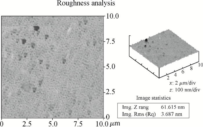
Fig. 1.
The surface of the H-terminated diamond material measured by AFM.
SEMICONDUCTOR DEVICES
Jianjun Zhou, Song Bai, Cen Kong, Xijiao Geng, Haiyan Lu, Yuechan Kong and Tangsheng Chen
Corresponding author: Zhou Jianjun, Email:jjzhouhawk@hotmail.com
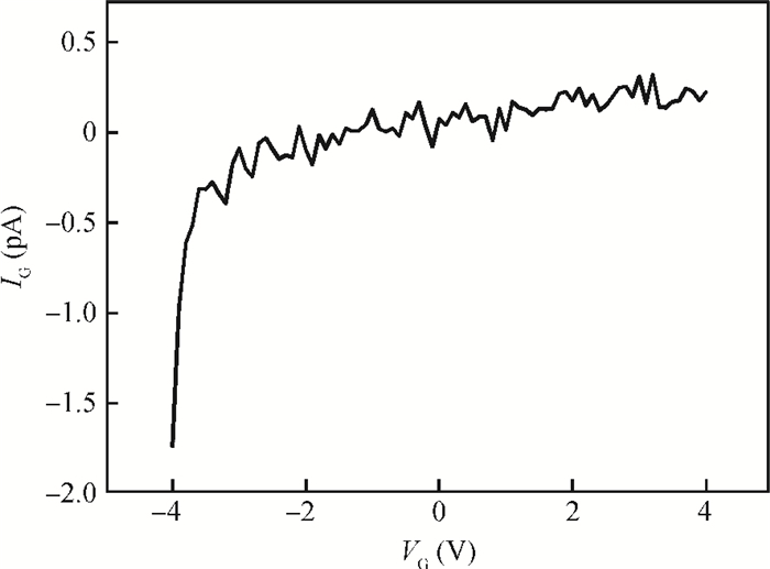
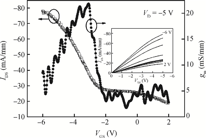
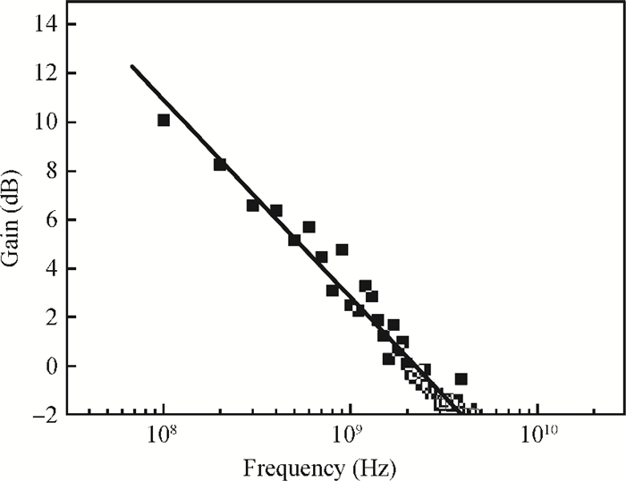
Abstract: Based on the hydrogen-terminated surface channel diamond material, a 1 μm gate length diamond metal-insulator-semiconductor field-effect transistor (MISFET) was fabricated. The gate dielectric Al2O3 was formed by naturally oxidated thin Al metal layer, and a less than 2 pA gate leakage current was obtained at gate bias between -4 V and 4 V. The DC characteristic of the diamond MISFET showed a drain-current density of 80 mA/mm at drain voltage of -5 V, and a maximum transconductance of 22 mS/mm at gate-source voltage of -3 V. With the small signal measurement, a current gain cutoff frequency of 2.1 GHz was also obtained.
| [1] |
Kasu M. Microwave operation of diamond field-effect transistor. NTT Technical Review, 2004, 2(6):19 https://www.ntt-review.jp/archive/ntttechnical.php?contents=ntr200406019.pdf
|
| [2] |
Collins T. The properties of diamond. Field J E, ed. London, UK:Academic, 1979
|
| [3] |
Koizumi S, Kamo M, Sato Y, et al. Growth and characterization of phosphorous doped (111) homoepitaxial diamond thin films. Appl Phys Lett, 1997, 71:1065 doi: 10.1063/1.119729
|
| [4] |
Sakaguchi I, Gamo M N, Kikuchi Y, et al. Sulfur:a donor dopant for n-type diamond semiconductors. Phys Rev B, 1999, 60:R2139 doi: 10.1103/PhysRevB.60.R2139
|
| [5] |
Hayashi K, Yamanaka S, Okushi H, et al. Study of the effect of hydrogen on transport properties in chemical vapor deposited diamond films by Hall measurements. Appl Phys Lett, 1996, 68:376 doi: 10.1063/1.116690
|
| [6] |
Nebel C E, Ertl F, Sauerer C, et al. Low temperature properties of the p-type surface conductivity of diamond. Diamond Relat Mater, 2002, 11:351 doi: 10.1016/S0925-9635(01)00586-6
|
| [7] |
Tsugawa K, Kitatani K, Noda H, et al. High-performance diamond surface-channel field effect transistors and their operation mechanism. Diamond Relat Mater, 1999, 8:927 doi: 10.1016/S0925-9635(98)00449-X
|
| [8] |
Yun Y, Maki T, Kobayashi T. Surface state density distribution of semiconducting diamond films measured from the Al/CaF2/i-diamond metal-insulator-semiconductor diodes and transistors. J Appl Phys, 1997, 82:3422 doi: 10.1063/1.365658
|
| [9] |
Kawarada H. Hydrogen-terminated diamond surface and interfaces. Surf Sci Rep, 1996, 26:205 doi: 10.1016/S0167-5729(97)80002-7
|
| [10] |
Matsudaira H, Miyamoto S, Ishizaka H, et al. Over 20 GHz cut-off frequency deep sub-micron gate diamond MISFET. IEEE Electron Device Lett, 2004, 25(7):480 doi: 10.1109/LED.2004.831200
|
| [11] |
Kasu M, Ueda K, Ye H, et al. 2 W/mm output power density at 1 GHz for diamond FETs. Electron Lett, 2005, 41(22):1249 doi: 10.1049/el:20053194
|
| [12] |
Ueda K, Kasu M, Yamauchi Y, et al. Diamond FET using high-quality polycrystalline diamond with fT of 45 GHz and fmax of 120 GHz. IEEE Electron Device Lett, 2006, 27(7):570 doi: 10.1109/LED.2006.876325
|
| [13] |
Moran D A J, Fox O J L, McLelland H, et al. Scaling of hydrogen-terminated diamond FETs to sub-100-nm gate dimensions. IEEE Electron Device Lett, 2011, 32(5):599 doi: 10.1109/LED.2011.2114871
|


Article views: 3193 Times PDF downloads: 24 Times Cited by: 0 Times
Received: 05 August 2012 Revised: 06 October 2012 Online: Published: 01 March 2013
| Citation: |
Jianjun Zhou, Song Bai, Cen Kong, Xijiao Geng, Haiyan Lu, Yuechan Kong, Tangsheng Chen. Research on the diamond MISFET[J]. Journal of Semiconductors, 2013, 34(3): 034006. doi: 10.1088/1674-4926/34/3/034006
****
J J Zhou, S Bai, C Kong, X J Geng, H Y Lu, Y C Kong, T S Chen. Research on the diamond MISFET[J]. J. Semicond., 2013, 34(3): 034006. doi: 10.1088/1674-4926/34/3/034006.

|
| [1] |
Kasu M. Microwave operation of diamond field-effect transistor. NTT Technical Review, 2004, 2(6):19 https://www.ntt-review.jp/archive/ntttechnical.php?contents=ntr200406019.pdf
|
| [2] |
Collins T. The properties of diamond. Field J E, ed. London, UK:Academic, 1979
|
| [3] |
Koizumi S, Kamo M, Sato Y, et al. Growth and characterization of phosphorous doped (111) homoepitaxial diamond thin films. Appl Phys Lett, 1997, 71:1065 doi: 10.1063/1.119729
|
| [4] |
Sakaguchi I, Gamo M N, Kikuchi Y, et al. Sulfur:a donor dopant for n-type diamond semiconductors. Phys Rev B, 1999, 60:R2139 doi: 10.1103/PhysRevB.60.R2139
|
| [5] |
Hayashi K, Yamanaka S, Okushi H, et al. Study of the effect of hydrogen on transport properties in chemical vapor deposited diamond films by Hall measurements. Appl Phys Lett, 1996, 68:376 doi: 10.1063/1.116690
|
| [6] |
Nebel C E, Ertl F, Sauerer C, et al. Low temperature properties of the p-type surface conductivity of diamond. Diamond Relat Mater, 2002, 11:351 doi: 10.1016/S0925-9635(01)00586-6
|
| [7] |
Tsugawa K, Kitatani K, Noda H, et al. High-performance diamond surface-channel field effect transistors and their operation mechanism. Diamond Relat Mater, 1999, 8:927 doi: 10.1016/S0925-9635(98)00449-X
|
| [8] |
Yun Y, Maki T, Kobayashi T. Surface state density distribution of semiconducting diamond films measured from the Al/CaF2/i-diamond metal-insulator-semiconductor diodes and transistors. J Appl Phys, 1997, 82:3422 doi: 10.1063/1.365658
|
| [9] |
Kawarada H. Hydrogen-terminated diamond surface and interfaces. Surf Sci Rep, 1996, 26:205 doi: 10.1016/S0167-5729(97)80002-7
|
| [10] |
Matsudaira H, Miyamoto S, Ishizaka H, et al. Over 20 GHz cut-off frequency deep sub-micron gate diamond MISFET. IEEE Electron Device Lett, 2004, 25(7):480 doi: 10.1109/LED.2004.831200
|
| [11] |
Kasu M, Ueda K, Ye H, et al. 2 W/mm output power density at 1 GHz for diamond FETs. Electron Lett, 2005, 41(22):1249 doi: 10.1049/el:20053194
|
| [12] |
Ueda K, Kasu M, Yamauchi Y, et al. Diamond FET using high-quality polycrystalline diamond with fT of 45 GHz and fmax of 120 GHz. IEEE Electron Device Lett, 2006, 27(7):570 doi: 10.1109/LED.2006.876325
|
| [13] |
Moran D A J, Fox O J L, McLelland H, et al. Scaling of hydrogen-terminated diamond FETs to sub-100-nm gate dimensions. IEEE Electron Device Lett, 2011, 32(5):599 doi: 10.1109/LED.2011.2114871
|

 WeChat ID
Journal of Semiconductors © 2017 All Rights Reserved 京ICP备05085259号-2

 DownLoad: