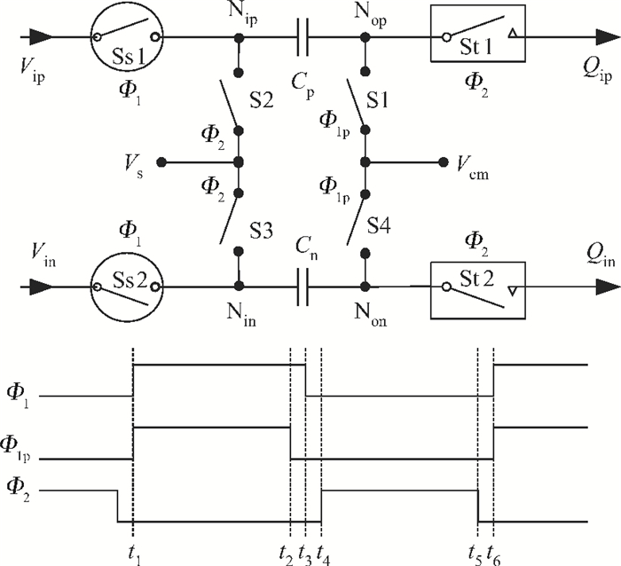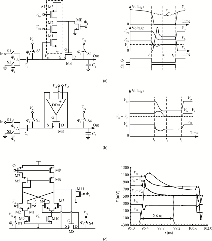
Fig. 1.
BCTs and operation waveforms. (a) BCT in Ref. [12]. (b) The proposed BCT. (c) Schematic and simulated waveform of the proposed BCT.
SEMICONDUCTOR INTEGRATED CIRCUITS
Zhenhai Chen1, 2, , Songren Huang1, 2, Hong Zhang3, Zongguang Yu1, 2 and Huicai Ji2
Corresponding author: Chen Zhenhai, diaoyuds@126.com
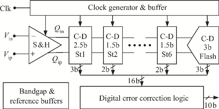
Abstract: A low power 10-bit 125-MSPS charge-domain (CD) pipelined analog-to-digital converter (ADC) based on MOS bucket-brigade devices (BBDs) is presented. A PVT insensitive boosted charge transfer (BCT) that is able to reject the charge error induced by PVT variations is proposed. With the proposed BCT, the common mode charge control circuit can be eliminated in the CD pipelined ADC and the system complexity is reduced remarkably. The prototype ADC based on the proposed BCT is realized in a 0.18 μm CMOS process, with power consumption of only 27 mW at 1.8-V supply and active die area of 1.04 mm2. The prototype ADC achieves a spurious free dynamic range (SFDR) of 67.7 dB, a signal-to-noise ratio (SNDR) of 57.3 dB, and an effective number of bits (ENOB) of 9.0 for a 3.79 MHz input at full sampling rate. The measured differential nonlinearity (DNL) and integral nonlinearity (INL) are +0.5/-0.3 LSB and +0.7/-0.55 LSB, respectively.
Keywords: pipelined analog-to-digital converter, charge domain, low power, charge transfer circuit, charge comparator
| [1] |
Cai X B, Li F L, Zhang C, et al. A 12 bit 100 MS/s pipelined analog to digital converter without calibration. Journal of Semiconductors, 2010, 31(11):100 http://www.jos.ac.cn/bdtxbcn/ch/reader/view_abstract.aspx?file_no=10050602&flag=1
|
| [2] |
Ali A, Morgan A, Dillon C, et al. A 16-bit 250-MS/s IF sampling pipelined ADC with background calibration. IEEE J Solid-State Circuits, 2010, 45(12):2602 doi: 10.1109/JSSC.2010.2073194
|
| [3] |
Payne R, Corsi M, Smith D, et al. A 16-bit 100 to 160 MS/s SiGe BiCMOS pipelined ADC with 100 dBFS SFDR. IEEE J Solid-State Circuits, 2010, 45(12):2613 doi: 10.1109/JSSC.2010.2074650
|
| [4] |
Zhou L R, Luo L, Ye F, et al. A 12 bit 100 MS/s pipelined ADC with digital background calibration. Journal of Semiconductors, 2010, 31(11):109 http://www.jos.ac.cn/bdtxbcn/ch/reader/view_abstract.aspx?file_no=10050602&flag=1
|
| [5] |
Peter B, Franz K, Claus K, et al. A 14 b 100 MS/s digitally self-calibrated pipelined ADC in 0.13μm CMOS. ISSCC Dig Tech Papers, 2006:224 http://ieeexplore.ieee.org/abstract/document/4030785
|
| [6] |
Murmann B, Boser B. A 12-b 75 MS/s pipelined ADC using open-loop residue amplifier. ISSCC Dig Tech Papers, 2003:330 http://ieeexplore.ieee.org/document/1234320/
|
| [7] |
Li J, Moon U. Background calibration techniques for multi-stage pipelined ADC's with digital redundancy. IEEE Trans Circuits Syst Ⅱ, 2003, 50(9):531 doi: 10.1109/TCSII.2003.816921
|
| [8] |
Sepke T, Fiorenza J K, Sodini C G, et al. Comparator-based switched-capacitor circuits for scaled CMOS technologies. ISSCC Dig Tech Papers, 2006:220 http://ieeexplore.ieee.org/articleDetails.jsp?arnumber=4014611
|
| [9] |
Brooks L, Lee H S. A zero-crossing based 8-bit 200 MS/s pipelined ADC. IEEE J Solid-State Circuits, 2007, 42(12):2677 doi: 10.1109/JSSC.2007.908770
|
| [10] |
Buchanan J E. Bucket brigade analog-to-digital converter. US Patent, No. 4072938, 1978
|
| [11] |
Berglund C N. Analog performance limitations of charge transfer dynamic shift registers. IEEE J Solid-State Circuits, 1971, 6(6):391 doi: 10.1109/JSSC.1971.1050209
|
| [12] |
Anthony M, Kohler E, Kurtze J, et al. A process-scalable low-power charge-domain 13-bit pipeline ADC. Symposium on VLSI Circuits, Dig Tech Papers, 2008:222 http://ieeexplore.ieee.org/iel5/4573021/4585928/04586015.pdf?arnumber=4586015
|
| [13] |
Frey W. Bucket-brigade device with improved charge transfer. IET Electron Lett, 1973, 9(25):588 doi: 10.1049/el:19730435
|
| [14] |
Anthony M, Kurtze J. Charge domain pipelined analog to digital converter. US Patent, No. 7570192, 2009
|
| [15] |
Yoshioka M, Kudo M, Gotoh K, et al. A 10 b 125 MS/s 40 mW pipelined ADC in 0.18μm CMOS. ISSCC Dig Tech Papers, 2005:282 http://dblp.uni-trier.de/db/conf/aspdac/aspdac2011.html#BaoWYCZ11
|
| [16] |
Pratap N S, Ashish K, Chandrajit D, et al. 20 mW, 125 Msps, 10 bit pipelined ADC in 65 nm standard digital CMOS process. IEEE CICC Dig Tech Papers, 2007:189 doi: 10.1088/1674-4926/34/3/035009
|
| [17] |
Cheol C H, Ju K Y, Joo K W, et al. A 10 b 120 MS/s 108 mW 0.18μm CMOS ADC with a PVT-insensitive current reference. Analog Integrated Circuits and Signal Processing, 2009, 61(58):115 http://ieeexplore.ieee.org/xpls/abs_all.jsp?arnumber=6800514
|
| [18] |
Lee K H, Lee S W, Kim Y J, et al. Ten-bit 100 MS/s 24.2 mW 0.8 mm2 0.18μm CMOS pipeline ADC based on maximal circuit sharing schemes. Electron Lett, 2009, 45(25):1296 doi: 10.1049/el.2009.2199
|
| [19] |
Shin C S, Ahn G C. A 10-bit 100-MS/s dual-channel pipelined ADC using dynamic memory effect cancellation technique. IEEE Trans Circuits Syst Ⅱ, 2011, 58(5):274 doi: 10.1109/TCSII.2011.2149130
|
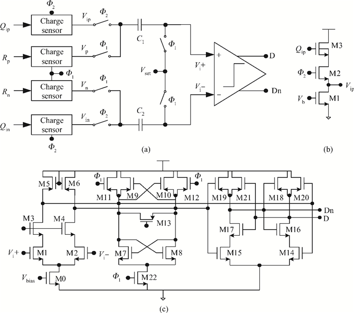
Table 1. Performance summary.

|
| [1] |
Cai X B, Li F L, Zhang C, et al. A 12 bit 100 MS/s pipelined analog to digital converter without calibration. Journal of Semiconductors, 2010, 31(11):100 http://www.jos.ac.cn/bdtxbcn/ch/reader/view_abstract.aspx?file_no=10050602&flag=1
|
| [2] |
Ali A, Morgan A, Dillon C, et al. A 16-bit 250-MS/s IF sampling pipelined ADC with background calibration. IEEE J Solid-State Circuits, 2010, 45(12):2602 doi: 10.1109/JSSC.2010.2073194
|
| [3] |
Payne R, Corsi M, Smith D, et al. A 16-bit 100 to 160 MS/s SiGe BiCMOS pipelined ADC with 100 dBFS SFDR. IEEE J Solid-State Circuits, 2010, 45(12):2613 doi: 10.1109/JSSC.2010.2074650
|
| [4] |
Zhou L R, Luo L, Ye F, et al. A 12 bit 100 MS/s pipelined ADC with digital background calibration. Journal of Semiconductors, 2010, 31(11):109 http://www.jos.ac.cn/bdtxbcn/ch/reader/view_abstract.aspx?file_no=10050602&flag=1
|
| [5] |
Peter B, Franz K, Claus K, et al. A 14 b 100 MS/s digitally self-calibrated pipelined ADC in 0.13μm CMOS. ISSCC Dig Tech Papers, 2006:224 http://ieeexplore.ieee.org/abstract/document/4030785
|
| [6] |
Murmann B, Boser B. A 12-b 75 MS/s pipelined ADC using open-loop residue amplifier. ISSCC Dig Tech Papers, 2003:330 http://ieeexplore.ieee.org/document/1234320/
|
| [7] |
Li J, Moon U. Background calibration techniques for multi-stage pipelined ADC's with digital redundancy. IEEE Trans Circuits Syst Ⅱ, 2003, 50(9):531 doi: 10.1109/TCSII.2003.816921
|
| [8] |
Sepke T, Fiorenza J K, Sodini C G, et al. Comparator-based switched-capacitor circuits for scaled CMOS technologies. ISSCC Dig Tech Papers, 2006:220 http://ieeexplore.ieee.org/articleDetails.jsp?arnumber=4014611
|
| [9] |
Brooks L, Lee H S. A zero-crossing based 8-bit 200 MS/s pipelined ADC. IEEE J Solid-State Circuits, 2007, 42(12):2677 doi: 10.1109/JSSC.2007.908770
|
| [10] |
Buchanan J E. Bucket brigade analog-to-digital converter. US Patent, No. 4072938, 1978
|
| [11] |
Berglund C N. Analog performance limitations of charge transfer dynamic shift registers. IEEE J Solid-State Circuits, 1971, 6(6):391 doi: 10.1109/JSSC.1971.1050209
|
| [12] |
Anthony M, Kohler E, Kurtze J, et al. A process-scalable low-power charge-domain 13-bit pipeline ADC. Symposium on VLSI Circuits, Dig Tech Papers, 2008:222 http://ieeexplore.ieee.org/iel5/4573021/4585928/04586015.pdf?arnumber=4586015
|
| [13] |
Frey W. Bucket-brigade device with improved charge transfer. IET Electron Lett, 1973, 9(25):588 doi: 10.1049/el:19730435
|
| [14] |
Anthony M, Kurtze J. Charge domain pipelined analog to digital converter. US Patent, No. 7570192, 2009
|
| [15] |
Yoshioka M, Kudo M, Gotoh K, et al. A 10 b 125 MS/s 40 mW pipelined ADC in 0.18μm CMOS. ISSCC Dig Tech Papers, 2005:282 http://dblp.uni-trier.de/db/conf/aspdac/aspdac2011.html#BaoWYCZ11
|
| [16] |
Pratap N S, Ashish K, Chandrajit D, et al. 20 mW, 125 Msps, 10 bit pipelined ADC in 65 nm standard digital CMOS process. IEEE CICC Dig Tech Papers, 2007:189 doi: 10.1088/1674-4926/34/3/035009
|
| [17] |
Cheol C H, Ju K Y, Joo K W, et al. A 10 b 120 MS/s 108 mW 0.18μm CMOS ADC with a PVT-insensitive current reference. Analog Integrated Circuits and Signal Processing, 2009, 61(58):115 http://ieeexplore.ieee.org/xpls/abs_all.jsp?arnumber=6800514
|
| [18] |
Lee K H, Lee S W, Kim Y J, et al. Ten-bit 100 MS/s 24.2 mW 0.8 mm2 0.18μm CMOS pipeline ADC based on maximal circuit sharing schemes. Electron Lett, 2009, 45(25):1296 doi: 10.1049/el.2009.2199
|
| [19] |
Shin C S, Ahn G C. A 10-bit 100-MS/s dual-channel pipelined ADC using dynamic memory effect cancellation technique. IEEE Trans Circuits Syst Ⅱ, 2011, 58(5):274 doi: 10.1109/TCSII.2011.2149130
|


Article views: 3188 Times PDF downloads: 25 Times Cited by: 0 Times
Received: 17 June 2012 Revised: 24 September 2012 Online: Published: 01 March 2013
| Citation: |
Zhenhai Chen, Songren Huang, Hong Zhang, Zongguang Yu, Huicai Ji. A 27-mW 10-bit 125-MSPS charge domain pipelined ADC with a PVT insensitive boosted charge transfer circuit[J]. Journal of Semiconductors, 2013, 34(3): 035009. doi: 10.1088/1674-4926/34/3/035009
****
Z H Chen, S R Huang, H Zhang, Z G Yu, H C Ji. A 27-mW 10-bit 125-MSPS charge domain pipelined ADC with a PVT insensitive boosted charge transfer circuit[J]. J. Semicond., 2013, 34(3): 035009. doi: 10.1088/1674-4926/34/3/035009.

|
| [1] |
Cai X B, Li F L, Zhang C, et al. A 12 bit 100 MS/s pipelined analog to digital converter without calibration. Journal of Semiconductors, 2010, 31(11):100 http://www.jos.ac.cn/bdtxbcn/ch/reader/view_abstract.aspx?file_no=10050602&flag=1
|
| [2] |
Ali A, Morgan A, Dillon C, et al. A 16-bit 250-MS/s IF sampling pipelined ADC with background calibration. IEEE J Solid-State Circuits, 2010, 45(12):2602 doi: 10.1109/JSSC.2010.2073194
|
| [3] |
Payne R, Corsi M, Smith D, et al. A 16-bit 100 to 160 MS/s SiGe BiCMOS pipelined ADC with 100 dBFS SFDR. IEEE J Solid-State Circuits, 2010, 45(12):2613 doi: 10.1109/JSSC.2010.2074650
|
| [4] |
Zhou L R, Luo L, Ye F, et al. A 12 bit 100 MS/s pipelined ADC with digital background calibration. Journal of Semiconductors, 2010, 31(11):109 http://www.jos.ac.cn/bdtxbcn/ch/reader/view_abstract.aspx?file_no=10050602&flag=1
|
| [5] |
Peter B, Franz K, Claus K, et al. A 14 b 100 MS/s digitally self-calibrated pipelined ADC in 0.13μm CMOS. ISSCC Dig Tech Papers, 2006:224 http://ieeexplore.ieee.org/abstract/document/4030785
|
| [6] |
Murmann B, Boser B. A 12-b 75 MS/s pipelined ADC using open-loop residue amplifier. ISSCC Dig Tech Papers, 2003:330 http://ieeexplore.ieee.org/document/1234320/
|
| [7] |
Li J, Moon U. Background calibration techniques for multi-stage pipelined ADC's with digital redundancy. IEEE Trans Circuits Syst Ⅱ, 2003, 50(9):531 doi: 10.1109/TCSII.2003.816921
|
| [8] |
Sepke T, Fiorenza J K, Sodini C G, et al. Comparator-based switched-capacitor circuits for scaled CMOS technologies. ISSCC Dig Tech Papers, 2006:220 http://ieeexplore.ieee.org/articleDetails.jsp?arnumber=4014611
|
| [9] |
Brooks L, Lee H S. A zero-crossing based 8-bit 200 MS/s pipelined ADC. IEEE J Solid-State Circuits, 2007, 42(12):2677 doi: 10.1109/JSSC.2007.908770
|
| [10] |
Buchanan J E. Bucket brigade analog-to-digital converter. US Patent, No. 4072938, 1978
|
| [11] |
Berglund C N. Analog performance limitations of charge transfer dynamic shift registers. IEEE J Solid-State Circuits, 1971, 6(6):391 doi: 10.1109/JSSC.1971.1050209
|
| [12] |
Anthony M, Kohler E, Kurtze J, et al. A process-scalable low-power charge-domain 13-bit pipeline ADC. Symposium on VLSI Circuits, Dig Tech Papers, 2008:222 http://ieeexplore.ieee.org/iel5/4573021/4585928/04586015.pdf?arnumber=4586015
|
| [13] |
Frey W. Bucket-brigade device with improved charge transfer. IET Electron Lett, 1973, 9(25):588 doi: 10.1049/el:19730435
|
| [14] |
Anthony M, Kurtze J. Charge domain pipelined analog to digital converter. US Patent, No. 7570192, 2009
|
| [15] |
Yoshioka M, Kudo M, Gotoh K, et al. A 10 b 125 MS/s 40 mW pipelined ADC in 0.18μm CMOS. ISSCC Dig Tech Papers, 2005:282 http://dblp.uni-trier.de/db/conf/aspdac/aspdac2011.html#BaoWYCZ11
|
| [16] |
Pratap N S, Ashish K, Chandrajit D, et al. 20 mW, 125 Msps, 10 bit pipelined ADC in 65 nm standard digital CMOS process. IEEE CICC Dig Tech Papers, 2007:189 doi: 10.1088/1674-4926/34/3/035009
|
| [17] |
Cheol C H, Ju K Y, Joo K W, et al. A 10 b 120 MS/s 108 mW 0.18μm CMOS ADC with a PVT-insensitive current reference. Analog Integrated Circuits and Signal Processing, 2009, 61(58):115 http://ieeexplore.ieee.org/xpls/abs_all.jsp?arnumber=6800514
|
| [18] |
Lee K H, Lee S W, Kim Y J, et al. Ten-bit 100 MS/s 24.2 mW 0.8 mm2 0.18μm CMOS pipeline ADC based on maximal circuit sharing schemes. Electron Lett, 2009, 45(25):1296 doi: 10.1049/el.2009.2199
|
| [19] |
Shin C S, Ahn G C. A 10-bit 100-MS/s dual-channel pipelined ADC using dynamic memory effect cancellation technique. IEEE Trans Circuits Syst Ⅱ, 2011, 58(5):274 doi: 10.1109/TCSII.2011.2149130
|

 WeChat ID
Journal of Semiconductors © 2017 All Rights Reserved 京ICP备05085259号-2

 DownLoad: