


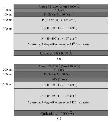
Fig. 1.
Schematics of the pn-diode structures with (a) growth of p-GaN epitaxy over p-(4H)SiC and (b) growth of p-GaN epitaxy over n-(4H)SiC with a 2 nm AlN interface layer
SEMICONDUCTOR DEVICES
Bose Srikanta and S K Mazumder
Corresponding author: Bose Srikanta, Email:sribose@ece.uic.edu, srknbose@gmail.com
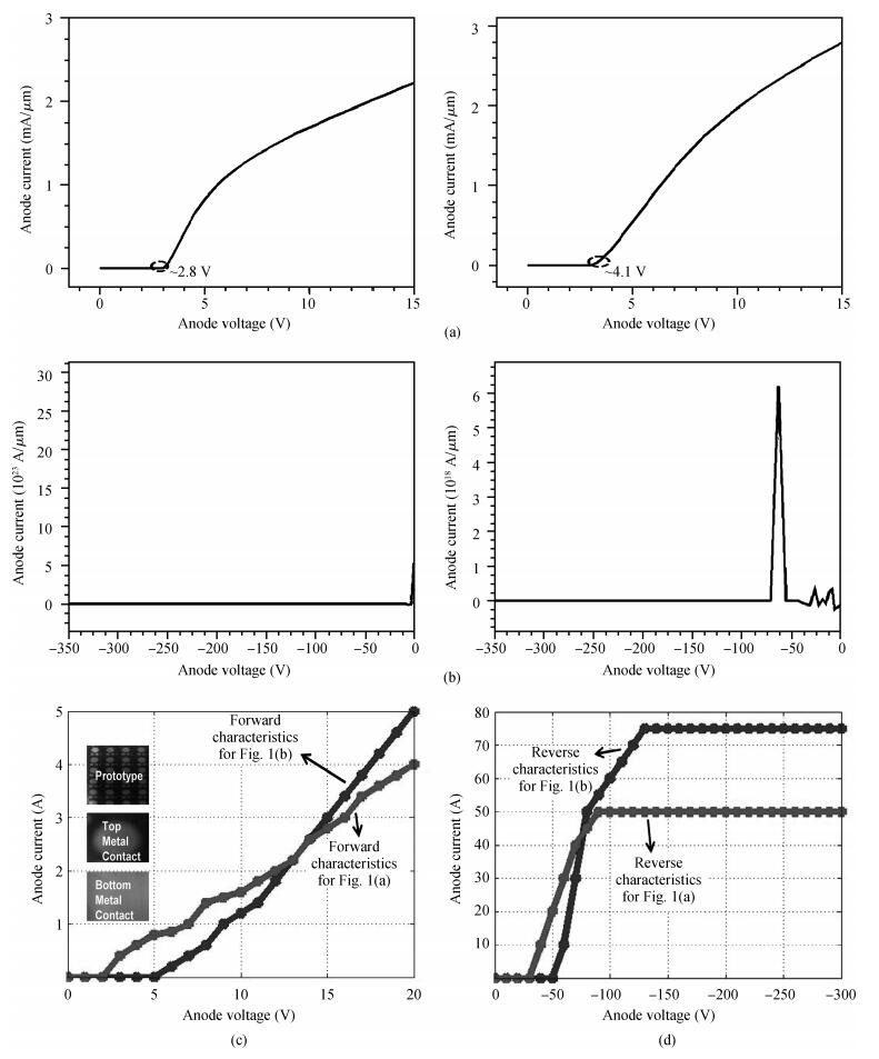
Abstract: We report the fabrication and characterization of a vertical pn power diode which is realized using two separate epitaxial-growth mechanisms:(a) p-GaN over p-(4H)SiC, and (b) p-GaN over n-(4H)SiC with AlN as the interface layer. In all of the cases, n+-doped (4H)SiC serves as the cathode substrate. Pd(200 Ǻ)/Au(10000 Ǻ) is used for the anode contact while Ni(1000 Ǻ) is used for the bottom cathode contact. The measured forward drop of the pn diode with AlN as the interface material is found to be around 5.1 V; whereas, it is 3 V for the other sample structure. The measured reverse-blocking voltage is found to be greater than 200 V.
Keywords: GaN, (4H)SiC, vertical pn power diode, power electronics
| [1] |
Bose S, Mazumder S K. Simulation study of optically triggered GaN/4H-SiC hetero-structure vertical NPN device. Government Microcircuit Applications and Critical Technology Conference (GOMACTech-10), Reno, NV, 2010 http://ieeexplore.ieee.org/document/5666324/keywords
|
| [2] |
Nam O, Bremser M, Zheleva T, et al. Lateral epitaxy of low defect density GaN layers via organometallic vapor phase epitaxy. Appl Phys Lett, 1997, 71:2638 doi: 10.1063/1.120164
|
| [3] |
Bose S, Mazumder S K. Atomistic and electrical simulations of a GaN-AlN-(4H)SiC heterostructure optically-triggered vertical power semiconductor device. Solid-State Electron, 2011, 62:5 doi: 10.1016/j.sse.2011.03.008
|
| [4] |
Feng Z C. Ⅲ-nitride devices and nanoengineering. London:Imperial College Press, 2008
|
| [5] | |
| [6] |
Sze S M, Ng K K. Physics of semiconductor devices. 3rd ed. New Jersey:John Wiley and Sons, 2007
|
| [7] |
Paxton A T, Sher A, Berding M, et al. How dislocations affect transport. J Electron Mater, 1994, 24:525 https://kclpure.kcl.ac.uk/portal/en/publications/how-dislocations-affect-transport(c0a59818-6e83-47a8-9061-2b1e7c993a9c).html
|
| [8] |
Claeys C, Simoen E. Defect control in advanced high-mobility substrates. J Phys:Conference Series, 2005, 10:125 doi: 10.1088/1742-6596/10/1/031
|


Article views: 2530 Times PDF downloads: 29 Times Cited by: 0 Times
Received: 12 September 2012 Revised: 24 October 2012 Online: Published: 01 April 2013
| Citation: |
Bose Srikanta, S K Mazumder. Fabrication and characterization of a GaN/(4H)SiC vertical pn power diode using direct and interfaced epitaxial-growth approaches[J]. Journal of Semiconductors, 2013, 34(4): 044001. doi: 10.1088/1674-4926/34/4/044001
****
B Srikanta, S K Mazumder. Fabrication and characterization of a GaN/(4H)SiC vertical pn power diode using direct and interfaced epitaxial-growth approaches[J]. J. Semicond., 2013, 34(4): 044001. doi: 10.1088/1674-4926/34/4/044001.

|
| [1] |
Bose S, Mazumder S K. Simulation study of optically triggered GaN/4H-SiC hetero-structure vertical NPN device. Government Microcircuit Applications and Critical Technology Conference (GOMACTech-10), Reno, NV, 2010 http://ieeexplore.ieee.org/document/5666324/keywords
|
| [2] |
Nam O, Bremser M, Zheleva T, et al. Lateral epitaxy of low defect density GaN layers via organometallic vapor phase epitaxy. Appl Phys Lett, 1997, 71:2638 doi: 10.1063/1.120164
|
| [3] |
Bose S, Mazumder S K. Atomistic and electrical simulations of a GaN-AlN-(4H)SiC heterostructure optically-triggered vertical power semiconductor device. Solid-State Electron, 2011, 62:5 doi: 10.1016/j.sse.2011.03.008
|
| [4] |
Feng Z C. Ⅲ-nitride devices and nanoengineering. London:Imperial College Press, 2008
|
| [5] | |
| [6] |
Sze S M, Ng K K. Physics of semiconductor devices. 3rd ed. New Jersey:John Wiley and Sons, 2007
|
| [7] |
Paxton A T, Sher A, Berding M, et al. How dislocations affect transport. J Electron Mater, 1994, 24:525 https://kclpure.kcl.ac.uk/portal/en/publications/how-dislocations-affect-transport(c0a59818-6e83-47a8-9061-2b1e7c993a9c).html
|
| [8] |
Claeys C, Simoen E. Defect control in advanced high-mobility substrates. J Phys:Conference Series, 2005, 10:125 doi: 10.1088/1742-6596/10/1/031
|

 WeChat ID
Journal of Semiconductors © 2017 All Rights Reserved 京ICP备05085259号-2

 DownLoad:

