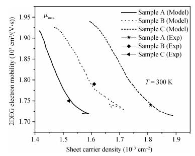
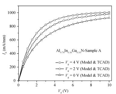
| [1] |
|
| [2] |
Mishra U K, Shen L, Kazior T E, et al. GaN-based RF power devices and amplifiers. Proc IEEE, 2008, 96:287 doi: 10.1109/JPROC.2007.911060 |
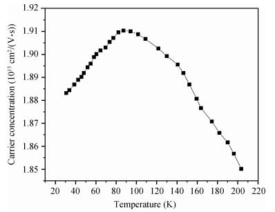
| [3] |
Shen L, Heikman S, Moran B, et al. AlGaN/AlN/GaN high-power microwave HEMT. IEEE Electron Device Lett, 2001, 22:457 doi: 10.1109/55.954910 |
| [4] |
Simin G, Koudymov A, Fatima H, et al. SiO 2/AlGaN/InGaN/GaN MOSDHFETs. IEEE Electron Device Lett, 2002, 23:458 doi: 10.1109/LED.2002.801316 |
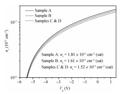
| [5] |
Balmer R S, Hilton K P, Nash K J, et al. AlGaN/GaN microwave HFET including a thin AlN carrier exclusion layer. Phys Status Solidi C, 2003, 0:2331 doi: 10.1002/(ISSN)1610-1642 |
| [6] |
Wang C M, Wang X L, Hu G X, et al. Influence of AlN interfacial layer on electrical properties of high-Al-content Al 0.45Ga 0.55N/GaN HEMT structure. Appl Surf Sci, 2006, 253:762 doi: 10.1016/j.apsusc.2006.01.017 |
| [7] |
Hashimoto S, Akita K, Tanabe T, et al. Study of two-dimensional electron gas in AlGaN channel HEMTs with high crystalline quality. Phys Status Solidi C, 2010, 7:1938 doi: 10.1002/pssc.v7:7/8 |
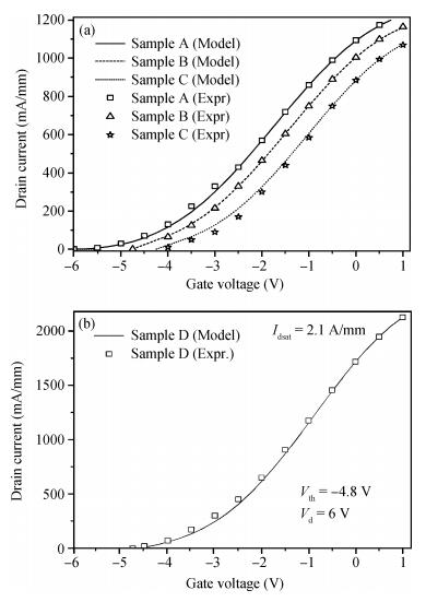
| [8] |
Medjdoub F, Carlin J F, Gonschorek M, et al. Can InAlN/GaN be an alternative to high power/high temperature AlGaN/GaN devices. IEDM Tech Dig, 2006:927
|
| [9] |
Wang H, Chung J, Gao X, et al. Al 2O 3 passivated InAlN/GaN HEMTs on SiC substrate with record current density and transconductance. Phys Status Solidi C, 2010, 7(10):2440 doi: 10.1002/pssc.200983899 |
| [10] |
Sun H, Alt A R, Benedickter H, et al. 205-GHz (Al, In)N/GaN HEMTs. IEEE Electron Device Lett, 2010, 31(9):957 doi: 10.1109/LED.2010.2055826 |
| [11] |
Wang R, Sanier P, Xing X, et al. Gate-recessed enhancement-mode InAlN/AlN/GaN HEMTs with 1.9 A/mm drain current density and 800 mS/mm transconductance. IEEE Electron Device Lett, 2010, 31(12):1383 doi: 10.1109/LED.2010.2072771 |
| [12] |
Wang R, Saunier P, Tang Y, et al. Enhancement-mode InAlN/AlN/GaN HEMTs with 10 -12 A/mm leakage current and 10 12 on/off current ratio. IEEE Electron Device Lett, 2011, 32(3):309 doi: 10.1109/LED.2010.2095494 |
| [13] |
Crespo A, Bellot M M, Chabak K D, et al. High-power Ka-band performance of AlInN/GaN HEMT with 9.8-nm-thin barrier. IEEE Electron Device Lett, 2010, 31(1):2 doi: 10.1109/LED.2009.2034875 |
| [14] |
Tang Y, Saunier P, Wang R, et al. High-performance monolithically integrated E/D mode InAlN/AlN/GaN HEMTs for mixed-signal applications. IEDM Tech Dig, 2010:30.4.1
|
| [15] |
Lee D S, Gao X, Guo S, et al. InAlN/GaN HEMTs with AlGaN back barriers. IEEE Electron Device Lett, 2011, 32(5):617 doi: 10.1109/LED.2011.2111352 |
| [16] |
Wang R, Li G, Laboutin O, et al. 210 GHz InAlN/GaN HEMTs with dielectric free passivation. IEEE Electron Device Lett, 2011, 32(7):892 doi: 10.1109/LED.2011.2147753 |
| [17] |
Cao Y, Wang K, Li G, et al. MBE growth of high conductivity single and multiple AlN/GaN heterojunctions. J Cryst Growth, 2011, 323(1):529 doi: 10.1016/j.jcrysgro.2010.12.047 |
| [18] |
Takayama T, Yuri M, Itoh K, et al. Analysis of phase-separation region in wurtzite group Ⅲ nitride quaternary material system using modified valence force field model. J Cryst Growth, 2001, 222(1/2):29
|
| [19] |
Ketteniss N, Khoshroo L R, Eickelkamp M, et al. Study on quaternary AlInGaN/GaN HFETs grown on sapphire substrates. Semicond Sci Technol, 2010, 25(7):075013 doi: 10.1088/0268-1242/25/7/075013 |
| [20] |
Lim T, Aidam R, Waltereit P, et al. GaN-based submicrometer HEMTs with lattice-matched InAlGaN barrier grown by MBE. IEEE Electron Device Lett, 2010, 31(7):671 doi: 10.1109/LED.2010.2048996 |
| [21] |
Hirayama H, Kinoshita A, Yamabi T, et al. Marked enhancement of 320-360 nm ultraviolet emission in quaternary In xAl yGa 1-x-yN with In-segregation effect. Appl Phys Lett, 2002, 80(2):207 doi: 10.1063/1.1433162 |
| [22] |
Asgari A, Kalafi M, Faraone L. A quasi-two-dimensional charge transport model of AlGaN/GaN high electron mobility transistors (HEMTs). Phys E, 2005, 28(4):491 doi: 10.1016/j.physe.2005.05.054 |
| [23] |
Cheng X, Wang Y. A surface-potential-based compact model for AlGaN/GaN MODFET. IEEE Trans Electron Devices, 2011, 58:448 doi: 10.1109/TED.2010.2089690 |
| [24] |
Khandelwal S, Goyal N, Fjeldly T A. A physics-based analytical model for 2DEG charge density in AlGaN/GaN HEMT devices. IEEE Tran Electron Devices, 2011, 58:3622 doi: 10.1109/TED.2011.2161314 |
| [25] |
Ketteniss N, Khoshroo L R, Eickelkamp M, et al. Study on quaternary AlInGaN/GaN HFETs grown on sapphire substrates. Semicond Sci Technol, 2010, 25(7):075013 doi: 10.1088/0268-1242/25/7/075013 |
| [26] |
Khoshroo L R, Ketteniss N, Mauder C, et al. Quaternary nitride heterostructure field effect transistors. Phys Status Solidi C, 2010, 7(7/8):2001
|
| [27] |
Wang R, Li G, Verma J, et al. 220-GHz quaternary barrier InAlGaN/AlN/GaN HEMTs. IEEE Electron Device Lett, 2011, 32(9):1215 doi: 10.1109/LED.2011.2158288 |
| [28] |
Kola S, Golio J M, Maracas G N. An analytical expression for Fermi level versus sheet carrier concentration for HEMT modeling. IEEE Electron Devices Lett, 1988, 9(3):136 doi: 10.1109/55.2067 |
| [29] |
Lee R R, Svensson S P, Lugli P. Pseudomorphic HEMT technology and Applications. Kluwer Academic Publishers, 1996:156
|
| [30] |
Ytterdal T, Cheng Y, Fjeldly T A. Device modelling for analog and RF circuit design. John Willey and Sons, 2003:31
|
| [31] |
Williams C K, Glisson T H, Hauser J R, et al. Energy bandgap and lattice constant contours of Ⅲ-Ⅴ quaternary alloys of the form A xB yC zD or AB xC yD z. J Electron Mater, 1978, 7(5):639 doi: 10.1007/BF02655439 |


 DownLoad: