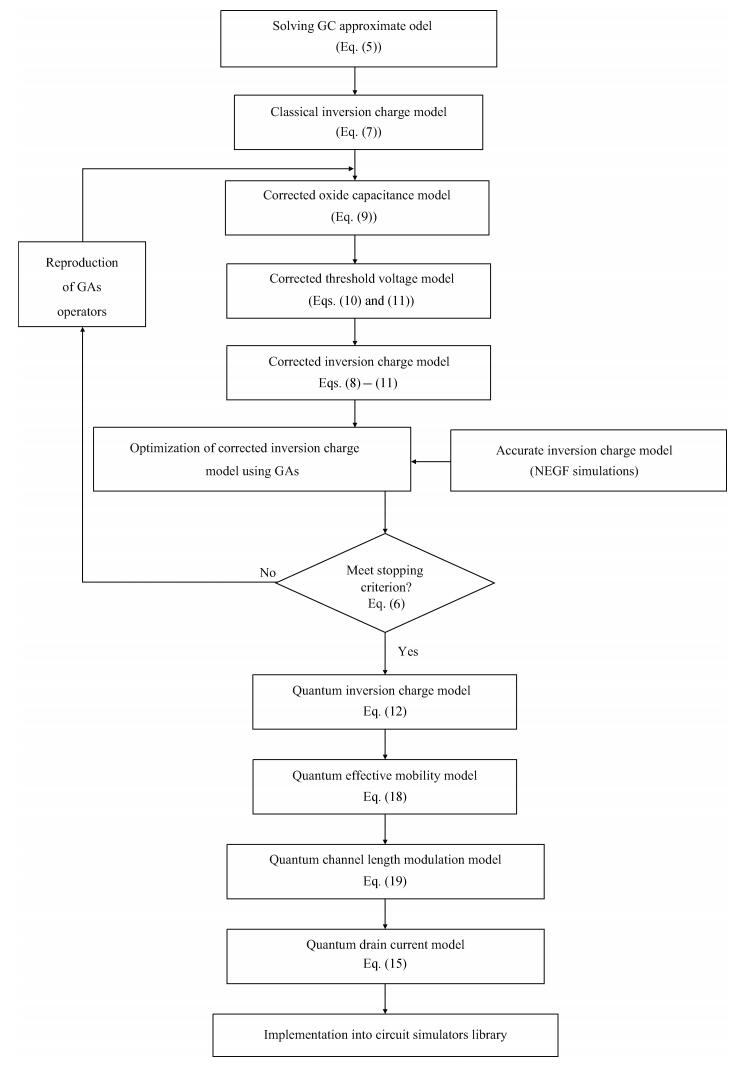
J. Semicond. > 2013, Volume 34 > Issue 4 > 044003

SEMICONDUCTOR DEVICES

A compact charge-based model to study the nanoscale undoped double gate MOSFETs for nanoelectronic circuit design using genetic algorithms

T. Bendib, F. Djeffal and D. Arar

+ Author Affiliations

 Corresponding author: F. Djeffal, Email:faycal.djeffal@univ-batna.dz, faycaldzdz@hotmail.com

DOI: 10.1088/1674-4926/34/4/044003

PDF

Abstract: The analytical modeling of nanoscale devices is an important area of computer-aided design for fast and accurate nanoelectronic design and optimization. In the present paper, a new approach for modeling semiconductor devices, nanoscale double gate DG MOSFETs, by use of the gradual channel approximation (GC) approach and genetic algorithm optimization technique (GA) is presented. The proposed approach combines the universal optimization and fitting capability of GA and the cost-effective optimization concept of quantum correction, to achieve reliable, accurate and simple compact models for nanoelectronic circuit simulations. Our compact models give good predictions of the quantum capacitance, threshold voltage shift, quantum inversion charge density and drain current. These models have been verified with 2D self-consistent results from numerical calculations of the coupled Poisson-Schrödinger equations. The developed models can also be incorporated into nanoelectronic circuit simulators to study the nanoscale CMOS-based devices without impact on the computational time and data storage.

Key words: nanoscalequantumgenetic algorithmanalytical model

As the MOSFET gate length enters the nanoscale field, short channel effects such as threshold voltage roll-off and drain-induced-barrier-lowering become increasingly significant, which limit the scaling capability of MOSFET design[1, 2]. Downscaling MOSFETs to their limits is a key challenge faced by the nanoelectronic industry. Therefore, new designs and structures become necessary to overcome these challenges. Multi-gate design, particularly the double gate (DG) MOSFETs (Fig. 1), are very important in nanoscale CMOS circuit design. This is mainly due to the superior control of the short channel effects (SCEs) because of the reduced influence of the drain voltage on the channel charge. Accurate information extraction about the current-voltage (I-V) characteristics requires the solution of Schrödinger and Poisson equations based on the non-equilibrium Green's function (NEGF) formalism, assuming quantum effects are fully accounted[3]. However, from the nanoscale CMOS circuit design point of view even a 2D solution of numerical NEGF is an overkill approach in term of both terms: complexity and computational cost[3]. In this regard, therefore, a high computational speed is necessary if the model is to be implemented in circuit simulators (PSPICE, CADENCE, ${\cdots}$). For analytical modeling of semiconductor devices, the gradual channel (GCA) model is widely used for analytical semiconductor device modeling. This model, based on the first two moments of Boltzman transport equation (BTE), is simple with powerful methods for device simulations. On the other hand, it is well known that the GCA model has not enough accuracy for the simulation of deep-submicrometer devices in which, rapid changes and confinement of eclectic field, and non-local effects such as velocity overshoot and quantum effects are pronounced[4-6]. Recently, several papers have been published to model the nanoscale DG MOSFET[7-13]. However, in these publications, simple and accurate closed expressions for quantum capacitance, channel length modulation and drain current were not provided, thus limiting the models which will be used by the designers.

Figure  1.  Schematic sketch of symmetrical DG MOSFET structure investigated in this study with channel doping $N_{\rm A}$ = 10$^{16}$ cm$^{-3}$, $t_{\rm si}$ represents silicon thickness and $t_{\rm ox}$ is the oxide thickness

In the present paper, we present an efficient and systematic technique for nanoscale DG MOSFETs modeling, where simple and accurate device models can be automatically achieved from a computational process to maximally reduce human trial and error efforts. The developed model should be able to correctly represent the I-V characteristics of the nanoscale device, and effectively capture the electrical behavior of the device due to process variations. In addition, the model should be formulated such that it can be conveniently incorporated into existing circuit simulators for high-level circuit simulation and yield design. Unlike the numerical models used to study the nanoscale structure, such as 2D numerical non-equilibrium Green's function (NEGF) formalism, which is complicated and requires a high computation time and storage memory, the proposed approach has a lower complexity and lower simulation time, which are the prerequisites of nanoelectronic circuit simulators.

Recently, artificial intelligence techniques (AI) have been recognized as an important approach in the semiconductor device computer-aided design area in addressing the growing challenges of designing the next generation of nanoelectronic devices, circuits, and systems[3, 9]. The AI-based methods represent important steps towards automating the device modeling process. However, because the genetic algorithms have to learn the device behavior from numerical or experimental databases without using existing device physical models like: drift-diffusion (D-D), hydrodynamic and gradual-channel approximation (HGCA), which makes the reliability of the AI-based model low and questionable. In GA, variables of a problem are represented as genes in a chromosome, and the chromosomes (population) are evaluated according to their fitness values. Given a random initial population GA operates in cycles called generations. The problem to be solved is defined in terms of an evaluation function (fitness function), which is used to evaluate the chromosomes. A chromosome evaluated as having a high fitness value is likely to be a good solution to the problem.

Implementation of GA requires the determination of six fundamental issues: chromosome representation, selection function, genetic operators, initialization, and evaluation function[14, 15].

One of the approaches for mapping between the accurate and approximate models is to correct the approximate model parameters so that the simulation results are based on an approximate model, and mimic the accurate simulation results. Based on the efficiency proven by NEGF for the modeling of nanoscale DG MOSFETs and the difficulty imposed at the moment by the constraints of the nanotechnology (sub-50 nm) to form an experimental database[3, 9], we have used the NEGF formalism as an accurate model.

The gradual channel approximation (GCA), which assumes that the quasi Fermi potential stays constant along the direction perpendicular to the channel, is used in our study as an approximated model. Accurate models for long channel double-gate MOSFETs[10, 16-18] have been recently developed using the conventional approach, showing good agreement with 2D numerical simulations. The inclusion of short-channel effects SCEs in undoped multiple gate MOS models, using physical equations and without decreasing the order of continuity of the devices, is still a modeling challenge. For devices with channel lengths shorter than 50 nm, the drift-diffusion mechanism may not be the dominant transport mechanism. Ballistic or quasiballistic transport may occur. Adequate models for nanoscale devices must consider the balllistic or quasi-ballistic regime[19, 20].

Breaking away from the premise of the GCA means that one needs to solve the Poisson equation given by

$ Δϕ(x,y)=qniεsie[ϕ(x,y)ϕF]/Vth,

$

(1)

where q is the electron charge, $n_{\rm i}$ is the silicon intrinsic concentration, $\varepsilon_{\rm si}$ is the silicon permittivity, $V_{\rm th}$ is the thermal voltage, $\phi (x, y)$ represents the 2D electrostatic potential distribution in the channel region, and $\phi_{\rm F}$ is the non-equilibrium quasi-Fermi level referenced to the Fermi level in the source, satisfying the following boundary conditions:

$ ϕF(0,y)=0,

$

(2)

$ ϕF(L,y)=Vds,

$

(3)

$V_{\rm ds}$ being the drain voltage. $\phi _{\rm F}$ can be approximated by a second order polynomial function, using Ref. [21], as

$ ϕF(x)=VdsL2x2.

$

(4)

The drain current of a symmetrical DG MOSFET assuming gradual channel approximation is given by

$ IDS=qμeff(x,y)n(x,y)dϕF(x)dx=qμeff(x,y)nie[ϕ(x,y)ϕF]dϕF(x)dx,

$

(5)

where $\mu_{\rm eff}$ is the effective electron mobility, and $n(x, y)$ represents the free charge concentration in the channel region.

As shown, the parameters $\mu_{\rm eff} (x, y)$, $n(x, y)$ and $\phi _{\rm F}(x)$ in Eq. (5) are correct for this purpose. In our approach, the genetic algorithm (GA) generates the optimal and corrected distribution of these parameters, which are inserted into the approximate model (GCA) to produce simulation results close to the accurate model (NEGF). Figure 2 shows the proposed GA-based approach block diagram.

Figure  2.  Flowchart of our charge-based computation approach

According to Eqs. (1) and (5), in a semiconductor device, the basic variables are electron distribution ($n)$, potential distribution (∅), quasi Fermi potential ($\phi _{\rm F})$ and the effective electron mobility $(\mu _{\rm eff} )$. Therefore, these electrical parameter distributions have been used for training and optimisation of GA to generate and optimize an accurate analytical model to study nanoscale DG MOSFETs. In the present study, a mean squared error of each parameter, Par, the $j_{\rm th}$ generation is taken as the fitness function,

$ f=1MVdsVgsTsiToxL[ParNUMParGAANAParNUM]2,

$

(6)

where f is the fitness value; Par$_{\rm GA-ANA} $ is the predicted parameter based on the GA and analytical computations; Par$_{\rm NUM}$ represents the target function (numerical results based on the 2D numerical, NEGF, simulation); and Mrepresents the number of samples (database size). It is aimed to minimize this fitness function, for each parameter, in order to develop accurate simple compact drain current model for nanoscale DG MOSFETs.

Taur in Ref. [22], has introduced a long channel model for the inversion charge of undoped DG MOSFET devices based on a 1D analytical solution of the Poisson equation incorporating only the mobile charge term as,

$ Qi=Cox[2CoxV2thQ0+(2CoxV2thQ0)2+4V2thln(1+eVgsVfbϕF+VT2Vth)],

$

(7)

where $C_{\rm ox} =\varepsilon _{\rm ox}/t_{\rm ox}$ represents the oxide capacitance per unit area, $V_{\rm fb}$ is the flat band voltage, $V_{\rm T}$ is the threshold voltage, and $Q_0$ is the charge coefficient given[22] by $Q_0 =(8V_{\rm th} \varepsilon _{\rm si} /t_{\rm si})$.

For silicon films thinner than 5 nm, quantum confinement should be considered; it leads to a reduction of the channel charge density and an increase of the threshold voltage.

From Eq. (7), we can see that an accurate model of the inversion charge depends mainly on the oxide capacitance and threshold voltage. Therefore, in order to develop an accurate charge model, new oxide capacitance and threshold voltage models, which include the quantum effects, should be introduced in Eq. (7).

Figure 3(a) shows the variation of the quantum oxide capacitance, $C_{\rm oxq}$, as function of channel thickness. This capacitance can be defined as the series combination of the $C_{\rm ox}$ and the inversion capacitance per unit area, and it is given by the following expression:

Figure  3.  (a) Classical and optimized quantum oxide capacitance versus film thickness. (b) Classical and quantum threshold voltage versus film thickness

$ Coxq=Cox1+CoxYIεs,

$

(8)

where $Y_{\rm I}$ represents the centroid. The latter mainly depends on the applied gate voltage and the channel thickness. In Ref. [5], the inversion layer at the centroid was modeled by assuming that the centroid was a quarter of the channel thickness. If we get $Y_{\rm I}/\varepsilon_{\rm s} =\xi _1 T_{\rm si}$, Equation (8) can be rewritten as

$ Coxq=Cox1+ξ1CoxTsi.

$

(9)

Figure 3(b) shows the variation of the quantum threshold voltage, $V_{\rm Tq}$, as a function of the channel thickness. This variation can be given as,

$ VTq=VT+δVTq,

$

(10)

with $\delta V_{\rm Tq}$ representing the threshold voltage shift due to the quantum effects, and it is given by,

$ δVTq=ξ2T2si,

$

(11)

where $\xi _1$ and $\xi _2$ are the fitting parameters which will be calculated using GAs as shown in Fig. 2.

Now, substituting the quantum oxide capacitance, $C_{\rm oxq}$, (Eq. (9)) and the quantum threshold voltage, $V_{\rm Tq}$, (Eq. (10)) into Eq. (7), a new inversion charge model can be given as,

$ Qiq=Coxq[2CoxqV2thQ0+(2CoxqV2thQ0)2+4V2thln(1+eVgsVfbϕF+VT+δVTq2Vth)].

$

(12)

The fitting parameters ($\xi _1$ and $\xi _2)$ in Eq. (12) can be extracted using Eq. (6).

The drain current for a DG MOSFET, including quantum effects, can be calculated from:

$ Idsq=μeffWLVdVsQiq(ϕF)dϕF,

$

(13)

where W is the channel width. Using Eqs. (12) and (13) and after some mathematical manipulations, the variation of the channel voltage as a function of the inversion charge can be written as,

$ dϕF=dQiq2dCoxqVth(dQiqQiq+dQiqQiq+2Q0).

$

(14)

Writing ${\rm d}\phi _{\rm F}$ as a function of Q and dQ in Eq. (13), and integrating between $Q_{\rm iqs}$ and $Q_{\rm iqd}$, we obtain:

$ Idsq=μeffWL[Q2iqsQ2iqdCoxq+4Vth(QiqsQiqd)+VthQ0ln(Q0+2QiqdQ0+2Qiqs)].

$

(15)

The charge densities at the source and the drain ends of the transistor $Q_{\rm iqs}$ and $Q_{\rm iqd}$ are respectively

$ Qiqs=Qiq(x=0)=Qiq(ϕF=0),

$

(16)

and

$ Qiqd=Qiq(x=L)=Qiq(ϕF=Vds).

$

(17)

For a transistor with a very thick body, the low-field mobility, $\mu _0$, does not change with thickness. However, the behavior of the effective electron mobility in very thin channel films, $T_{\rm si}$ less than 10 nm, tends to decrease[23]. In this case, the in-depth average values of the electron mobility and the effective electric field weighted by the electron distribution are given[24] by

$ μeffμ01+(EeffE0)δ=11+ηQiq2εsiE0,Eeff=Qiq2εsi,

$

(18)

where $E_0$ represents an applied eclectic field, which is considered in our study as the fitting parameter. This is calculated using the GAs (Fig. 2), $\varepsilon _{\rm si}$ as the silicon permittivity and $\eta$ is an empirical fitting parameter $\eta$ = 0.001.

For an applied drain-source voltage, more than the saturation voltage ($V_{\rm sat})$, the velocity is practically at its saturation value in a region near to the drain end. Inside this region, channel length modulation, region of length $\Delta L$ and the inversion charge are relatively constant, and the conventional transport equations (like: BTE, GCA, D-D) break down. If we apply the 2D Poisson equation in the channel region to study the channel length modulation[25], then $\Delta L$ can be obtained as,

$ ΔL=λlnϕd+ϕ2dϕ2dsat+(λθvsatμeff)2ϕdsat+λθvsatμeff,

$

(19)

where $\phi_{\rm d}$ is the drain channel voltage, $\phi _{\rm dsat}$ represents the saturation drain channel voltage, $\lambda$ is the natural length that depends only on the device structure, $\nu _{\rm sat}$ represents the electron saturation velocity near the drain end and θ is a fitting parameter where $\theta =2$. (The parameters of Eq. (19) are well defined in Ref. [25]). So, for $V_{\rm ds} \leqslant V_{\rm sat}$ the channel length modulation trends to zero, we can write the effective channel length as,

$ Le=LΔL.

$

(20)

In the drain current compact model (15), we replace channel length L by the effective channel length value (20) in order to include the channel length modulation effect.

For the purpose of GA-based optimization of Eq. (12), routines and programs for GA computation were developed using MATLAB 7.2 and all simulations were carried out on a Pentium Ⅳ, 3 GHz, 1 GB RAM computer. For the implementation of the GA, tournament selection is employed which selects each parent by choosing individuals at random, and then choosing the best individual out of that set to be a parent. Scattered crossover creates a random binary vector. It then selects the genes where the vector is united from the first parent, and the genes where the vector is zero from the second parent, and combines the genes to form the child. In our case, the crossover rate and the mutation rate are equal to 0.8 and 0.2 respectively. An optimization process was performed for a population size of 20 and a maximum number of generations equal to 100, for which stabilization of the fitness function was obtained. The obtained results of the proposed approach are presented for the studied device in two-dimensional space. The transistor length is 20 nm with 20 mesh points and its thickness is 5 nm with 5 mesh points. Therefore, simulation data are 2D matrixes of 20 × 5. The quantum simulations, self-consistent computations, have been carried out using 2D Silvaco and nano-MOS2.5 numerical simulator tools[26, 27].

Figure 4 shows the inversion charge density versus the gate-source voltage for a nanoscale undoped DG MOSFET. The increase and the shift of the inversion charge density due to the QM effect are well predicted by our model, given in Eq. (12). For below threshold voltage and in the subthreshold regime, quantum and classical inversion charge densities are close to each other. However, for a high gate-source voltage, the electrons are strongly confined in the direction perpendicular to the Si-SiO2 interface due to the increasing influence of the vertical electric field component. Figure 4 presents the influence of film thickness on the electron concentration distribution, in which the quantum distribution of charge is obtained by coupling Schrödinger's equation to Poisson's equation. Note that the carrier profile is modified, where the most of the carriers flow in the middle of the film, not at the interfaces. In Fig. 5, an excellent fit was found between our inversion charge model and the numerical Poisson-Schrödinger self-consistent (NEGF) simulation.

Figure  4.  Influence of the film thickness on the electron concentration distribution
Figure  5.  Classical and corrected quantum inversion charge versus gate-source voltage

Figure 6 presents comparisons between the target data (NEGF) and drain current data calculated by our model, Eq. (15), for both nanoscale DG MOSFET designs. We can see that the proposed model provides a good agreement for a very wide interval of geometrical and physical parameters for both the investigated nanoscale DG MOSFETs in comparison with numerical simulations. Hence, the proposed compact model can be used to predict other combinations of input variables ($V_{\rm gs}$, $V_{\rm ds}$, L, etc.) in full range. This last observation shows the applicability of the GA technique to study the nanoscale DG MOSFETs using a long channel compact current model.

Figure  6.  Numerical (symbols) and calculated (solid lines) drain current versus drain voltage

The forgoing results show that our model makes it feasible to include quantum effects accurately and generally in a nanoelectronic device simulation. In order to show a comparison between the proposed model and other approaches in the field of nano-CMOS circuit simulation, Table 1 shows that the neural method (AI-based method) is a behavioral approach of modeling where the neural model is given as a black-box and defined by 3 different blocks: an input vector-weight matrix and activation function-output vector, in addition, the analytical model proposed by Hariharan et al.[8] is more complex, includes several fitting parameters, and does not take into account the very thin channel effects. Contrary, in our approach, the developed model is an accurate simple analytical closed expression that includes the channel length modulation, the very thin channel effects and 2 global optimized fitting parameters ($\xi _1 =$ 1.72 × 10$^{11}$ and $\xi _2 =$ 5.32 × 10$^{-15})$. Therefore, the proposed model can be easily used by circuit simulation programs such as PSPICE for more accurate predictions of nanoscale DG MOSFET characteristics.

Table  1.  Comparison between the various approaches of modelling of the nano-DGMOSFET for L = 20 nm, $T_{\rm si}$ = 3 nm and $T_{\rm ox}$ = 1 nm
DownLoad: CSV  | Show Table

In this paper, a new analytical model that includes quantum and channel length modulation effects for undoped nanoscale DG MOSFETs is presented. The 2D P-S self-consistent computation and gradual channel approaches are used as accurate and approximate models, respectively. In the proposed approach, the Genetic Algorithm technique is used for mapping parameters of the gradual channel model into a new space. With mapped parameters, the GCA model is capable of producing results for an accurate 2D numerical simulation. The presented analytical models for threshold voltage, threshold voltage shift, quantum oxide capacitance, inversion charge density and drain current overcome problems using classical models. The proposed models have several advantages such as accuracy, simplicity and applicability for a wide device dimension range. The proposed models can be extended to include hot carrier and degradation effects. However, new models and analytical expressions should be developed in this case. The encouraging obtained results have indicated that the proposed closed analytical form is particularly suitable for incorporatedion in electronic device simulators to study nanoscale CMOS circuits.


[1]
The International Technology Roadmap for Semiconductors, 2007. Online Available: http//public.itrs.net
[2]
Djeffal F, Ghoggali Z, Dibi Z, et al. Analytical analysis of nanoscale multiple gate MOSFETs including effects of hot-carrier induced interface charges. Microelectron Reliab, 2009, 49:337
[3]
Djeffal F, Chahdi M, Benhaya A, et al. An approach based on neural computation to simulate the nanoscale CMOS circuits:ap-plication to the simulation of CMOS inverter. Solid-State Elec-tron, 2007, 51:48 doi: 10.1016/j.sse.2006.12.004
[4]
Stern F. Self-consistent results for n-type Si inversion layers. Phys Rev B, 1972, 5:4891 doi: 10.1103/PhysRevB.5.4891
[5]
Baccarani G, Reggiani S. A compact double-gate MOSFET model comprising quantum-mechanical and nonstatic effects. IEEE Trans Electron Devices, 1999, 46:1656 doi: 10.1109/16.777154
[6]
Chen Q, Meindl J D. Nanoscale metal oxide semiconductor field effect transistors:scaling limits and opportunities. Nanotechnology, 2004, 15:8549
[7]
Lopez-Villanueva J A, Cartujo-Cassinello P, Gamiz F, et al. Effects of the inversion layer centroid on the performance of DG MOSFETs. IEEE Trans Electron Devices, 2000, 47:141 doi: 10.1109/16.817579
[8]
Hariharan V, Thakker R, Singh K, et al. Drain current model for nanoscale double-gate MOSFETs. Solid-State Electron, 2009, 53:1001 doi: 10.1016/j.sse.2009.05.008
[9]
Djeffal F, Abdi M A, Dibi Z, et al. A neural approach to study the scaling capability of the undoped double-gate and cylindrical gate all around MOSFETs. Mater Sci & Eng B, 2007, 27:1111
[10]
Reyboz M, Rozeau O, Poiroux T, et al. An explicit analytical charge-based model of undoped independent double gate MOSFET. Solid-State Electron, 2006, 50:1276 doi: 10.1016/j.sse.2006.05.019
[11]
Lazaro A, ANe B, Moldovan O, et al. A compact quantum model of nanoscale double-gate metal-oxide-semiconductor field-effect transistor for high frequency and noise simulations. J Appl Phys, 2006, 100:084320 doi: 10.1063/1.2360379
[12]
Nae B, Lazaro A, Iñiguez B. High frequency and noise model of gate-all-around metal-oxide-semiconductor field-effect transistors. J Appl Phys, 2009, 105:074505 doi: 10.1063/1.3093884
[13]
Bentrcia T, Djeffal F, Benhaya A. Continuous analytic Ⅰ-Ⅴ model for GS DG MOSFETs including hot-carrier degradation effects. Journal of Semiconductors, 2012, 33:014001: doi: 10.1088/1674-4926/33/1/014001
[14]
Goldberg D E. Genetic algorithms in search, optimization, and machine learning reading. MA:Addison-Wesley, 1989
[15]
Painton L, Campbell J. Genetic algorithms in optimization of system reliability. IEEE Trans Reliab, 1995, 44:172 doi: 10.1109/24.387368
[16]
Iñiguez B, Fjeldly T A, Lázaro A, et al. Compact-modeling solutions for nanoscale double-gate and gate-all-around MOSFETs. IEEE Trans Electron Devices, 2006, 53:2128 doi: 10.1109/TED.2006.881007
[17]
Xiong S, King T J, Bokor J. A comparison study of symmetric ultrathin body double gate devices with metal source/drain and doped source/drain. IEEE Trans Electron Devices, 2005, 52:1859 doi: 10.1109/TED.2005.852893
[18]
Taur Y, Liang X, Wang W, et al. A continuous analytic drain current model for double gate MOSFETs. IEEE Electron Device Lett, 2004, 25:107 doi: 10.1109/LED.2003.822661
[19]
Datta S, Assad F, Lundstrom M S. The Si MOSFET from a transmission viewpoint. Superlattices and Microstructures, 1998, 23:771 doi: 10.1006/spmi.1997.0563
[20]
Naveh Y, Likharev K K. Shrinking limits of silicon MOSFETs:numerical study of 10 nm scale devices. Superlattices and Microstructures, 2000, 27:111 doi: 10.1006/spmi.1999.0807
[21]
Chen Q, Harrell E M, Meindl J D. A physical short-channel threshold voltage model for undoped symmetric double-gate MOSFETs. IEEE Trans Electron Devices, 2003, 50:1631 doi: 10.1109/TED.2003.813906
[22]
Taur Y. Analytic solutions of charge and capacitance in symmetric and asymmetric double-gate MOSFETs. IEEE Trans Electron Devices, 2001, 48:2861 doi: 10.1109/16.974719
[23]
Reggiani S, Gnani E, Gnudi A, et al. Low-field electron mobility model for ultrathin-body SOI and double-gate MOSFETs with extremely small silicon thickness. IEEE Trans Electron Devices, 2007, 54:2204 doi: 10.1109/TED.2007.902899
[24]
Munteanu D, Autran J L, Loussier X, et al. Quantum short-channel compact modelling of drain-current in double-gate MOSFET. Solid-State Electron, 2006, 50:680 doi: 10.1016/j.sse.2006.03.038
[25]
Lime F, Iñiguez B, Moldovan O. A quasi two-dimensional compact drain current model for undoped symmetric double gate MOSFETs including short-channel effects. IEEE Trans Electron Devices, 2008, 55:1441 doi: 10.1109/TED.2008.921980
[26]
ATLAS: 2D Device Simulator, SILVACO International, 2008
[27]
Ren Z, Venugopal R, Goasguen S, et al. NanoMOS2.5:a two-dimensional simulator for quantum transport in double-gate MOSFETs. IEEE Trans Electron Devices, 2003, 50:1914 doi: 10.1109/TED.2003.816524
Fig. 1.  Schematic sketch of symmetrical DG MOSFET structure investigated in this study with channel doping $N_{\rm A}$ = 10$^{16}$ cm$^{-3}$, $t_{\rm si}$ represents silicon thickness and $t_{\rm ox}$ is the oxide thickness

Fig. 2.  Flowchart of our charge-based computation approach

Fig. 3.  (a) Classical and optimized quantum oxide capacitance versus film thickness. (b) Classical and quantum threshold voltage versus film thickness

Fig. 4.  Influence of the film thickness on the electron concentration distribution

Fig. 5.  Classical and corrected quantum inversion charge versus gate-source voltage

Fig. 6.  Numerical (symbols) and calculated (solid lines) drain current versus drain voltage

Table 1.   Comparison between the various approaches of modelling of the nano-DGMOSFET for L = 20 nm, $T_{\rm si}$ = 3 nm and $T_{\rm ox}$ = 1 nm

[1]
The International Technology Roadmap for Semiconductors, 2007. Online Available: http//public.itrs.net
[2]
Djeffal F, Ghoggali Z, Dibi Z, et al. Analytical analysis of nanoscale multiple gate MOSFETs including effects of hot-carrier induced interface charges. Microelectron Reliab, 2009, 49:337
[3]
Djeffal F, Chahdi M, Benhaya A, et al. An approach based on neural computation to simulate the nanoscale CMOS circuits:ap-plication to the simulation of CMOS inverter. Solid-State Elec-tron, 2007, 51:48 doi: 10.1016/j.sse.2006.12.004
[4]
Stern F. Self-consistent results for n-type Si inversion layers. Phys Rev B, 1972, 5:4891 doi: 10.1103/PhysRevB.5.4891
[5]
Baccarani G, Reggiani S. A compact double-gate MOSFET model comprising quantum-mechanical and nonstatic effects. IEEE Trans Electron Devices, 1999, 46:1656 doi: 10.1109/16.777154
[6]
Chen Q, Meindl J D. Nanoscale metal oxide semiconductor field effect transistors:scaling limits and opportunities. Nanotechnology, 2004, 15:8549
[7]
Lopez-Villanueva J A, Cartujo-Cassinello P, Gamiz F, et al. Effects of the inversion layer centroid on the performance of DG MOSFETs. IEEE Trans Electron Devices, 2000, 47:141 doi: 10.1109/16.817579
[8]
Hariharan V, Thakker R, Singh K, et al. Drain current model for nanoscale double-gate MOSFETs. Solid-State Electron, 2009, 53:1001 doi: 10.1016/j.sse.2009.05.008
[9]
Djeffal F, Abdi M A, Dibi Z, et al. A neural approach to study the scaling capability of the undoped double-gate and cylindrical gate all around MOSFETs. Mater Sci & Eng B, 2007, 27:1111
[10]
Reyboz M, Rozeau O, Poiroux T, et al. An explicit analytical charge-based model of undoped independent double gate MOSFET. Solid-State Electron, 2006, 50:1276 doi: 10.1016/j.sse.2006.05.019
[11]
Lazaro A, ANe B, Moldovan O, et al. A compact quantum model of nanoscale double-gate metal-oxide-semiconductor field-effect transistor for high frequency and noise simulations. J Appl Phys, 2006, 100:084320 doi: 10.1063/1.2360379
[12]
Nae B, Lazaro A, Iñiguez B. High frequency and noise model of gate-all-around metal-oxide-semiconductor field-effect transistors. J Appl Phys, 2009, 105:074505 doi: 10.1063/1.3093884
[13]
Bentrcia T, Djeffal F, Benhaya A. Continuous analytic Ⅰ-Ⅴ model for GS DG MOSFETs including hot-carrier degradation effects. Journal of Semiconductors, 2012, 33:014001: doi: 10.1088/1674-4926/33/1/014001
[14]
Goldberg D E. Genetic algorithms in search, optimization, and machine learning reading. MA:Addison-Wesley, 1989
[15]
Painton L, Campbell J. Genetic algorithms in optimization of system reliability. IEEE Trans Reliab, 1995, 44:172 doi: 10.1109/24.387368
[16]
Iñiguez B, Fjeldly T A, Lázaro A, et al. Compact-modeling solutions for nanoscale double-gate and gate-all-around MOSFETs. IEEE Trans Electron Devices, 2006, 53:2128 doi: 10.1109/TED.2006.881007
[17]
Xiong S, King T J, Bokor J. A comparison study of symmetric ultrathin body double gate devices with metal source/drain and doped source/drain. IEEE Trans Electron Devices, 2005, 52:1859 doi: 10.1109/TED.2005.852893
[18]
Taur Y, Liang X, Wang W, et al. A continuous analytic drain current model for double gate MOSFETs. IEEE Electron Device Lett, 2004, 25:107 doi: 10.1109/LED.2003.822661
[19]
Datta S, Assad F, Lundstrom M S. The Si MOSFET from a transmission viewpoint. Superlattices and Microstructures, 1998, 23:771 doi: 10.1006/spmi.1997.0563
[20]
Naveh Y, Likharev K K. Shrinking limits of silicon MOSFETs:numerical study of 10 nm scale devices. Superlattices and Microstructures, 2000, 27:111 doi: 10.1006/spmi.1999.0807
[21]
Chen Q, Harrell E M, Meindl J D. A physical short-channel threshold voltage model for undoped symmetric double-gate MOSFETs. IEEE Trans Electron Devices, 2003, 50:1631 doi: 10.1109/TED.2003.813906
[22]
Taur Y. Analytic solutions of charge and capacitance in symmetric and asymmetric double-gate MOSFETs. IEEE Trans Electron Devices, 2001, 48:2861 doi: 10.1109/16.974719
[23]
Reggiani S, Gnani E, Gnudi A, et al. Low-field electron mobility model for ultrathin-body SOI and double-gate MOSFETs with extremely small silicon thickness. IEEE Trans Electron Devices, 2007, 54:2204 doi: 10.1109/TED.2007.902899
[24]
Munteanu D, Autran J L, Loussier X, et al. Quantum short-channel compact modelling of drain-current in double-gate MOSFET. Solid-State Electron, 2006, 50:680 doi: 10.1016/j.sse.2006.03.038
[25]
Lime F, Iñiguez B, Moldovan O. A quasi two-dimensional compact drain current model for undoped symmetric double gate MOSFETs including short-channel effects. IEEE Trans Electron Devices, 2008, 55:1441 doi: 10.1109/TED.2008.921980
[26]
ATLAS: 2D Device Simulator, SILVACO International, 2008
[27]
Ren Z, Venugopal R, Goasguen S, et al. NanoMOS2.5:a two-dimensional simulator for quantum transport in double-gate MOSFETs. IEEE Trans Electron Devices, 2003, 50:1914 doi: 10.1109/TED.2003.816524
1

Analytical model for the effects of the variation of ferrolectric material parameters on the minimum subthreshold swing in negative capacitance capacitor

Raheela Rasool, Najeeb-ud-Din, G. M. Rather

Journal of Semiconductors, 2019, 40(12): 122401. doi: 10.1088/1674-4926/40/12/122401

2

Compact analytical model for single gate AlInSb/InSb high electron mobility transistors

S. Theodore Chandra, N.B. Balamurugan, G. Subalakshmi, T. Shalini, G. Lakshmi Priya, et al.

Journal of Semiconductors, 2014, 35(11): 114003. doi: 10.1088/1674-4926/35/11/114003

3

Analytical modeling and simulation of germanium single gate silicon on insulator TFET

T. S. Arun Samuel, N. B. Balamurugan

Journal of Semiconductors, 2014, 35(3): 034002. doi: 10.1088/1674-4926/35/3/034002

4

In situ TEM/SEM electronic/mechanical characterization of nano material with MEMS chip

Yuelin Wang, Tie Li, Xiao Zhang, Hongjiang Zeng, Qinhua Jin, et al.

Journal of Semiconductors, 2014, 35(8): 081001. doi: 10.1088/1674-4926/35/8/081001

5

Modeling and simulation of centroid and inversion charge density in cylindrical surrounding gate MOSFETs including quantum effects

P. Vimala, N. B. Balamurugan

Journal of Semiconductors, 2013, 34(11): 114001. doi: 10.1088/1674-4926/34/11/114001

6

An analytical model of the electric field distributions of buried superjunction devices

Haimeng Huang, Xingbi Chen

Journal of Semiconductors, 2013, 34(6): 064006. doi: 10.1088/1674-4926/34/6/064006

7

Analytical modeling of drain current and RF performance for double-gate fully depleted nanoscale SOI MOSFETs

Rajiv Sharma, Sujata Pandey, Shail Bala Jain

Journal of Semiconductors, 2012, 33(2): 024001. doi: 10.1088/1674-4926/33/2/024001

8

A two-dimensional analytical-model-based comparative threshold performance analysis of SOI-SON MOSFETs

Sanjoy Deb, Saptarsi Ghosh, N Basanta Singh, A K De, Subir Kumar Sarkar, et al.

Journal of Semiconductors, 2011, 32(10): 104001. doi: 10.1088/1674-4926/32/10/104001

9

Gate current modeling and optimal design of nanoscale non-overlapped gate to source/drain MOSFET

Ashwani K. Rana, Narottam Chand, Vinod Kapoor

Journal of Semiconductors, 2011, 32(7): 074001. doi: 10.1088/1674-4926/32/7/074001

10

SPICE compatible analytical electron mobility model for biaxial strained-Si-MOSFETs

Amit Chaudhry, J. N. Roy, S. Sangwan

Journal of Semiconductors, 2011, 32(5): 054001. doi: 10.1088/1674-4926/32/5/054001

11

Mathematical modeling of nanoscale MOS capacitance in the presence of depletion and energy quantization in a poly-silicon gate

Amit Chaudhry, J. N. Roy

Journal of Semiconductors, 2010, 31(11): 114001. doi: 10.1088/1674-4926/31/11/114001

12

Nanoscale strained-Si MOSFET physics and modeling approaches: a review

Amit Chaudhry, J. N. Roy, Garima Joshi

Journal of Semiconductors, 2010, 31(10): 104001. doi: 10.1088/1674-4926/31/10/104001

13

Dual Material Gate SOI MOSFET with a Single Halo

Li Zunchao, Jiang Yaolin, Wu Jianmin

Chinese Journal of Semiconductors , 2007, 28(3): 327-331.

14

Modeling of Gate Tunneling Current for Nanoscale MOSFETs with High-k Gate Stacks

Wang Wei, Sun Jianping, Gu Ning

Chinese Journal of Semiconductors , 2006, 27(7): 1170-1176.

15

Analytical Model for the Piecewise Linearly Graded Doping Drift Region in LDMOS

Sun Weifeng, Yi Yangbo, Lu Shengli, Shi Longxing

Chinese Journal of Semiconductors , 2006, 27(6): 976-981.

16

An Analytical Model for the Surface Electrical Field Distribution and Optimization of Bulk-Silicon Double RESURF Devices

Li Qi, Li Zhaoji, Zhang Bo

Chinese Journal of Semiconductors , 2006, 27(7): 1177-1182.

17

SOI MOSFET Model Parameter Extraction via a Compound Genetic Algorithm

Li Ruizhen, Li Duoli, Du Huan, Hai Chaohe, Han Zhengsheng, et al.

Chinese Journal of Semiconductors , 2006, 27(5): 796-803.

18

Neural-Network-Based Charge Density Quantum Correction of Nanoscale MOSFETs

Li Zunchao, Jiang Yaolin, Zhang Ruizhi

Chinese Journal of Semiconductors , 2006, 27(3): 438-442.

19

An Analytical Threshold Voltage Model for Fully Depleted SOI MOSFETs

Li Ruizhen, Han Zhengsheng

Chinese Journal of Semiconductors , 2005, 26(12): 2303-2308.

20

Analytical Modeling of Threshold Voltage for Double-Gate MOSFET Fully Comprising Quantum Mechanical Effects

Zhang Dawei, Tian Lilin,and Yu Zhiping

Chinese Journal of Semiconductors , 2005, 26(3): 429-435.

  • Search

    Advanced Search >>

    GET CITATION

    T. Bendib, F. Djeffal, D. Arar. A compact charge-based model to study the nanoscale undoped double gate MOSFETs for nanoelectronic circuit design using genetic algorithms[J]. Journal of Semiconductors, 2013, 34(4): 044003. doi: 10.1088/1674-4926/34/4/044003
    T. Bendib, F. Djeffal, D. Arar. A compact charge-based model to study the nanoscale undoped double gate MOSFETs for nanoelectronic circuit design using genetic algorithms[J]. J. Semicond., 2013, 34(4): 044003. doi: 10.1088/1674-4926/34/4/044003.
    shu

    Export: BibTex EndNote

    Article Metrics

    Article views: 2337 Times PDF downloads: 15 Times Cited by: 0 Times

    History

    Received: 06 September 2012 Revised: 19 October 2012 Online: Published: 01 April 2013

    Catalog

      Email This Article

      User name:
      Email:*请输入正确邮箱
      Code:*验证码错误
      T. Bendib, F. Djeffal, D. Arar. A compact charge-based model to study the nanoscale undoped double gate MOSFETs for nanoelectronic circuit design using genetic algorithms[J]. Journal of Semiconductors, 2013, 34(4): 044003. doi: 10.1088/1674-4926/34/4/044003 ****T. Bendib, F. Djeffal, D. Arar. A compact charge-based model to study the nanoscale undoped double gate MOSFETs for nanoelectronic circuit design using genetic algorithms[J]. J. Semicond., 2013, 34(4): 044003. doi: 10.1088/1674-4926/34/4/044003.
      Citation:
      T. Bendib, F. Djeffal, D. Arar. A compact charge-based model to study the nanoscale undoped double gate MOSFETs for nanoelectronic circuit design using genetic algorithms[J]. Journal of Semiconductors, 2013, 34(4): 044003. doi: 10.1088/1674-4926/34/4/044003 ****
      T. Bendib, F. Djeffal, D. Arar. A compact charge-based model to study the nanoscale undoped double gate MOSFETs for nanoelectronic circuit design using genetic algorithms[J]. J. Semicond., 2013, 34(4): 044003. doi: 10.1088/1674-4926/34/4/044003.

      A compact charge-based model to study the nanoscale undoped double gate MOSFETs for nanoelectronic circuit design using genetic algorithms

      DOI: 10.1088/1674-4926/34/4/044003
      More Information
      • Corresponding author: F. Djeffal, Email:faycal.djeffal@univ-batna.dz, faycaldzdz@hotmail.com
      • Received Date: 2012-09-06
      • Revised Date: 2012-10-19
      • Published Date: 2013-04-01

      Catalog

        /

        DownLoad:  Full-Size Img  PowerPoint
        Return
        Return